bility (EMC) regulation, an efficient component-level TLU mea-surement setup with bipolar (underdamped sinusoidal) trigger is developed in this paper. A blocking diode and a current-limiting resistance, which are generally suggested to be used in the TLU measurement setup with bipolar trigger, are investigated for their impacts to both the bipolar trigger waveforms and the TLU immunity of the device under test (DUT). All the experimental results have been successfully verified with device simulation. Finally, a TLU measurement setup without a current-blocking diode but with a small current-limiting resistance, which can accurately evaluate the TLU immunity of CMOS ICs with neither overestimation nor electrical-over-stress damage to the DUT dur-ing the TLU test, is suggested. The suggested measurement setup has been verified with silicon-controlled-rectifier test structures and real circuitry (ring oscillator) fabricated in 0.25-µm CMOS technology.
Index Terms—Holding voltage, latch-up, silicon-controlled rectifier (SCR), system-level electrostatic discharge (ESD) test, transient-induced latch-up (TLU).
I. INTRODUCTION
T
RANSIENT-INDUCED latch-up (TLU) has attracted more attention [1]–[11] than before in state-of-the-art CMOS technologies such as RF, system-on-chip (SOC), mixed signal, and multiple power supplies. So far, several transient stimuli have been demonstrated to be possible trigger sources in initiating TLU [10]–[16]. Bipolar (underdamped sinusoidal) trigger voltage [10]–[12] on the power lines of CMOS ICs, in particular, has become the main concern because it deter-mines the TLU immunity of CMOS ICs under the system-level electrostatic discharge (ESD) test [17] for electromagnetic compatibility (EMC) regulation. “Bipolar” means that the po-larity of the voltage waveform can be varied with time repeat-edly between positive and negative. During the system-level ESD test, the electrical products must sustain an ESD level of±8 kV (±15 kV) under the contact-discharge (air-discharge)
test mode to achieve the immunity requirement of “level 4.” Such high-energy ESD-induced noises, however, often cause TLU on CMOS ICs inside the electrical/electronic products,
Manuscript received November 11, 2005; revised May 7, 2006. This work was supported by Himax Technologies, Inc., Taiwan, R.O.C.
The authors are with the Nanoelectronics and Gigascale Systems Laboratory, Institute of Electronics, National Chiao-Tung University, Hsinchu 300, Taiwan, R.O.C. (e-mail: [email protected]).
Digital Object Identifier 10.1109/TDMR.2006.882203
Fig. 1. Measurement setup of the system-level ESD test with indirect contact-discharge test mode [17]. The ESD gun zapping on the HCP could cause TLU events on all the CMOS ICs inside the EUT.
leading to the shutdown or malfunction of the equipment under test (EUT). Fig. 1 shows the measurement setup of the system-level ESD test with the indirect contact-discharge test mode [17]. When the ESD gun zaps to the horizontal coupling plane (HCP), all the CMOS ICs inside the EUT will be disturbed due to the high ESD-coupled energy, as shown in the inset of Fig. 1. For example, the measuredVDDtransient waveform on one (CMOS IC#1) of the CMOS ICs inside the EUT during an ESD voltage of −1000 V zapping on the HCP is shown in Fig. 2. Clearly, the power line (the VDD pin) of CMOS IC#1 no longer maintains its normal voltage level (+2.5 V) but acts as a bipolar transient voltage with a negative peak voltage of
−13 V. Such bipolar transient voltage on the power lines of
CMOS ICs can easily trigger on TLU [18], [19], resulting in either soft failure (e.g., loss of data logic state) or destructive failure (e.g., the chip burns out) in the CMOS ICs, even though such TLU-sensitive CMOS ICs have already met the requirements of the quasi-static latch-up test standard [20]. For example, with a higher ESD voltage of −3000 V zapping on the HCP, the measuredVDD andIDD transient waveforms on CMOS IC#1 are shown in Fig. 3. With a large transient peak voltage of±60 V on the power line of CMOS IC#1, TLU will be initiated with rapidly increasing transient currentIDD. After the ESD-induced disturbance onVDD,IDDis kept at a high cur-rent of 80 mA, andVDDis pulled down to the latch-up holding voltage of 1.8 V in a low-impedance latch-up state. Thus, the TLU reliability issue under the system-level ESD test is indeed
Fig. 2. Measured VDD transient waveform on one (CMOS IC#1) of the CMOS ICs inside the EUT under an ESD voltage of−1000 V zapping on the HCP. TheVDD waveform acts as a bipolar transient voltage due to the disturbance of the high ESD-coupled energy.
Fig. 3. MeasuredVDDandIDDtransient waveforms on CMOS IC#1 with an ESD voltage of−3000 V zapping on the HCP. With a large transient peak voltage of±60 V, TLU is triggered on (IDDis kept at a high current of 80 mA) after the ESD-induced disturbance onVDD.
crucial, and the related measurement setup to evaluate the TLU immunity of CMOS ICs must be developed.
However, during the realistic system-level ESD test, it could be rather complicated or difficult to directly evaluate the TLU immunity of a “single” CMOS IC inside the EUT. To solve such problem, a component-level TLU measurement setup with bipolar trigger waveform [10]–[12] is utilized. This measure-ment setup has the advantage of easily evaluating the TLU immunity of a single IC by monitoring the voltage/current waveforms through an oscilloscope. More importantly, with the ability of generating a bipolar trigger voltage, it can accurately simulate how a CMOS IC will be disturbed by ESD-generated noises under the system-level ESD test.
The purpose of this paper is to evaluate an efficient TLU measurement setup with bipolar trigger, which can accurately
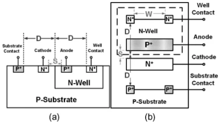
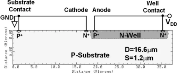
Fig. 4. (a) Device cross-sectional view and (b) layout top view of the SCR structure in CMOS process for TLU measurements. This test structure can simulate the parasitic SCR in real CMOS ICs.
evaluate the TLU immunity of CMOS ICs under the system-level ESD test. A current-blocking diode and a current-limiting resistance, which are generally suggested to be used in the TLU measurement setup with bipolar trigger, are investigated to find their impacts to both the bipolar trigger waveforms and the TLU immunity of the device under test (DUT). All the experimental results can be successfully verified with two-dimensional (2-D) device simulation (MEDICI). Finally, a TLU measurement setup without a blocking diode but with a small current-limiting resistance is suggested. This suggested measurement setup can accurately evaluate the TLU immunity of CMOS ICs without overestimation. All the experimental results have been verified in silicon with silicon-controlled rectifier (SCR) test structures and the real circuitry (ring oscillator) fabricated in 0.25-µm CMOS technology.
II. COMPONENT-LEVELTLU MEASUREMENTSETUP
An SCR structure is used as the test structure for TLU measurement because the occurrence of latch-up results from the parasitic SCR in CMOS ICs. The device cross-sectional view and layout top view of the SCR structure are sketched in Fig. 4(a) and (b), respectively. The geometrical parameters
D, S, and W represent the distances between the well edge
and the well (substrate) contact, the anode and the cathode, and the adjacent contacts, respectively. In order to consider the layout dependences, the SCR structures with two sets of layout parameters (D = 16.6 µm, S = 1.2 µm, and W = 22.5 µm,
andD = 16.6 µm, S = 20 µm, and W = 22.5 µm) are used
in this paper. All the SCR structures have been fabricated in 0.25-µm salicided CMOS technology.
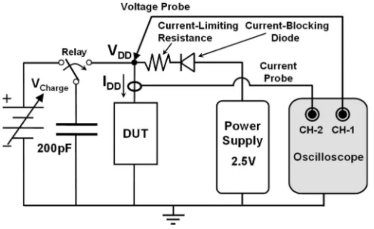
Several component-level measurement setups to evaluate TLU immunity of CMOS ICs have been developed [10]–[15]. In order to accurately simulate the ESD-induced noises on the power lines of CMOS ICs under the system-level ESD test, a component-level TLU measurement setup with bipolar trigger voltage [10]–[12] is utilized in this paper. The typical TLU measurement setup with bipolar trigger is sketched in Fig. 5 [10]–[12]. The charging voltageVChargehas two different polarities: positive(VCharge> 0) and negative (VCharge< 0). The positive (negative)VChargecan generate the positive-going (negative-going) bipolar trigger noises on the power pins of the
Fig. 5. Component-level TLU measurement setup with bipolar trigger [10]–[12]. It can accurately simulate how a CMOS IC will be disturbed by the ESD-generated noises under the system-level ESD test.
DUT. A 200-pF capacitor used in the machine model (MM) [21] ESD test is employed as the charging capacitor. The SCR device shown in Fig. 4 is used as the DUT, where the p+ anode (n+cathode) and the n+well (p+ substrate) contact are connected together to VDD (ground).IDD is the total current flowing into the p+anode and the n+well contact of the SCR. TheIDDcurrent magnitude and waveform are measured by a separated current probe. The current-blocking diode, which is used to prevent the capacitor-discharged current from flowing into the power supply (Agilent E3631A), is used to avoid possible overestimation of the TLU immunity of the DUT [10], [11]. The current-limiting resistance is used to avoid electrical-over-stress (EOS) damage to the DUT under a high-current latch-up state [12].
For a TLU measurement setup with a current-limiting resis-tance of 5Ω but without a current-blocking diode, the measured
VDD andIDD transient responses withVCharges of −3, −6, and+13 V are shown in Fig. 6(a), (b), and (c), respectively. The DUT under an initialVDDbias of 2.5 V is the SCR with specified layout parameters ofD = 16.6 µm, S = 1.2 µm, and W = 22.5 µm. With a smaller VCharge of−3 V, VDD acts as the intended bipolar trigger just similar to that measured in Fig. 2 under the system-level ESD test. Meanwhile, TLU does not occur due to a rather small VCharge (only−3 V) because
IDDdoes not increase after applying the bipolar trigger voltage onVDD. However, with a larger negative (positive)VChargeof
−6 V (+13 V), TLU can be initiated, as shown in Fig. 6(b)
[Fig. 6(c)]. Thus,IDD significantly increases up to 120 mA, andVDDis pulled down to a latch-up holding voltage of 1.6 V. By using this TLU measurement setup with bipolar trigger voltage, the measuredVDDandIDD waveforms in Fig. 6 can simulate the ESD-disturbedVDDandIDDwaveforms in Figs. 2 (no TLU) and 3 (TLU occurs) under the system-level ESD test.
III. PHYSICALMECHANISM OFTLU
Two different TLU-triggering currents have been men-tioned, namely 1) transient displacement currentIDs[16] and 2) sweep-back current ISb [18], [19]. IDs results from a rapid increase ofVDD with time (e.g., power-on transition or
VDD overshooting), and it is proportional to the increasing
Fig. 6. For the TLU measurement setup with a current-limiting resistance of 5Ω but without a current-blocking diode, the measured VDDandIDDtransient responses withVCharges of (a)−3, (b) −6, and (c) +13 V.
rate of VDD (dVDD/dt) and the n-well/p-substrate junction capacitance in bulk CMOS technology.ISb results from VDD switching from negative to positive voltage level (e.g., bipolar transient noises on VDD), and it correlates closely with the damping frequency and damping factor of bipolar transient noises on the power pins of CMOS ICs [22]. It has been clari-fied thatISbcan initiate TLU more easily thanIDs[12], [22].
The detailed physical mechanisms ofISb-induced TLU un-der bipolar transient noises on the power pins of CMOS ICs can be explained by the measured VDD and IDD transient responses in Fig. 6(b) and (c). For the negative-going bipolar trigger in Fig. 6(b), the n-well/p-substrate junction will switch from its original reversed-biased state to a forward-biased state whenVDD drops from its normal operating voltage (+2.5 V) to below 0 V. While VDD continues to drop to the nega-tive peak voltage(−VPeak), the largest forward-biased n-well/ p-substrate junction can generate the forward peak current, leading to a large number of minority holes (electrons) stored in the n-well (p-substrate) region. Afterward, whenVDDreturns from−VPeakto its normal operating voltage of+2.5 V, these stored minority holes (electrons) will be “swept back” to the p-substrate (n-well) region, where they originally came from. As a result, the sweep-back currentISbis formed. OnceISbis large enough to activate either a vertical p-n-p or a lateral n-p-n bipolar junction transistor (BJT) in the p-n-p-n latch-up path, TLU can be initiated, andIDDwill significantly increase. Due to the occurrence of TLU,IDDis kept at a high-current latch-up state (120 mA) with a pull-downVDD(∼1.6 V), as shown in Fig. 6(b). Thus,−VPeakis an important factor to determineISb because−VPeakdetermines how many stored minority carriers will be swept back. A larger (i.e., more negative)−VPeak can generate a largerISb, so TLU can be initiated more easily.
For the positive-going bipolar trigger in Fig. 6(c), the n-well/p-substrate junction is always reversed biased whenVDD initially increases from its normal operating voltage (+2.5 V) to a positive peak voltage(+VPeak). Meanwhile, only IDs or a junction leakage current can be found within the p-n-p-n latch-up path. However, TLU will not be initiated by IDs or the junction leakage current becauseIDD is negligible while
VDDinitially increases from+2.5 V to +VPeak(inducedIDs). TLU can be initiated by ISb because IDD simultaneously increases with VDD while VDD increases from −VPeak to +2.5 V (induced ISb). Thus, it can be verified that ISb can initiate TLU more easily thanIDs.
IV. EXPERIMENTALRESULTS
Although the TLU measurement setup with bipolar trigger can accurately simulate the practical system-level ESD event, both the bipolar trigger waveforms and the TLU immunity of CMOS ICs are strongly dependent on the current-blocking diode and the current-limiting resistance. To clarify this issue, TLU measurement setups that combine two kinds of current-blocking diodes, fast recovery (PR1507) and general purpose (1N4007), with various current-limiting resistances (0, 5, 10, 20, and 30 Ω) are investigated to find their impacts to both the bipolar trigger waveforms and the TLU immunity of the DUT. Both the PR1507 and 1N4007 diodes have a very
high reverse breakdown voltage (BV) of 1000 V. Thus, for
VCharge< 1000 V, the PR1507 or 1N4007 diode can certainly prevent the discharge current from flowing into the power supply without junction breakdown.
A. Dependences of the Current-Blocking Diode and Current-Limiting Resistance on the Bipolar
Trigger Waveforms
The SCR structure with layout parameters ofD = 16.6 µm, S = 1.2 µm, and W = 22.5 µm shown in Fig. 4 is used to
investigate the influences of the current-blocking diode and the current-limiting resistance on the bipolar trigger waveform. Furthermore, the charging voltage sourceVChargeis set to be as small as+8 V for a positive VCharge and−3 V for a negative
VChargeto prevent the occurrence of TLU, so the bipolar trigger waveform onVDDcan be clearly observed.
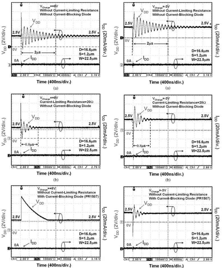
1) PositiveVCharge: With a positiveVChargeof+8 V, when there is neither a current-blocking diode nor a current-limiting resistance in the TLU measurement setup, the measuredVDD andIDDtransient waveforms are shown in Fig. 7(a). TheVDD waveform reveals the intended positive-going bipolar trigger with a damping frequency of ∼10 MHz. Afterward, when a current-limiting resistance of 20Ω is added to the TLU mea-surement setup without a current-blocking diode, the damping factor of theVDD waveform obviously increases, as shown in Fig. 7(b). The initial positive peak voltage ofVDDtakes about 2.5 µs to be fully attenuated in Fig. 7(a) and only 0.8 µs in
Fig. 7(b). Furthermore, if a current-blocking diode (PR1507) is added to the measurement setup without a current-limiting re-sistance, theVDDwaveform no longer reveals an underdamped bipolar waveform but an overdamped unipolar waveform instead, as shown in Fig. 7(c). When the initially stored positive charges in the charging capacitor (200 pF) are discharged through the relay into the DUT and power supply, these positive charges are blocked by the current-blocking diode from flowing into the power supply, so the current-blocking diode acts as a large equivalent resistance (open circuit) to these positive charges. As shown in Fig. 7(b), a current-limiting resistance of 20 Ω increases the damping factor of the VDD waveform, so the equivalent large resistance of the current-blocking diode tremendously increases the damping factor to result in an overdamped unipolarVDD waveform, as shown in Fig. 7(c).
2) NegativeVCharge: With a negativeVChargeof−3 V, the measured VDD transient waveforms are similar to that of the positiveVCharge case. For example, the measuredVDD wave-form is a negative-going bipolar trigger when there is neither a current-blocking diode nor a current-limiting resistance in the measurement setup, as shown in Fig. 8(a). Additionally, the damping factor of this measuredVDD waveform will increase if an additional current-limiting resistance of 20Ω is added to the measurement setup, as shown in Fig. 8(b). However, unlike the VDD waveform in the positive VCharge case in Fig. 7(c), which is an overdamped unipolar waveform, theVDDwaveform in Fig. 8(c) is an underdamped bipolar waveform if there is a current-blocking diode (PR1507) and no current-limiting resis-tance. When the initially stored negative charges in the charging
Fig. 7. MeasuredVDDandIDDtransient waveforms with a positiveVCharge
of+8 V. The TLU measurement setup with (a) neither the current-blocking diode nor the current-limiting resistance, (b) a current-limiting resistance of 20Ω but without a current-blocking diode, and (c) a current-blocking diode (PR1507) but without a current-limiting resistance.
Fig. 8. MeasuredVDDandIDDtransient waveforms with a negativeVCharge
of−3 V. The TLU measurement setup with (a) neither the current-blocking diode nor the current-limiting resistance, (b) a current-limiting resistance of 20Ω but without a current-blocking diode, and (c) a current-blocking diode (PR1507) but without a current-limiting resistance.
capacitor (200 pF) are discharged into the power supply, the current-blocking diode is seen as a forward-biased diode by these negative charges, so the current-blocking diode acts as a small equivalent resistance (short circuit) to these negative charges. Thus, similar to the current-limiting resistance of 20Ω in Fig. 8(b), the small equivalent resistance of the current-blocking diode also leads to a larger damping factor of theVDD waveform in Fig. 8(c).
B. Dependences of the Current-Blocking Diode and Current-Limiting Resistance on the TLU Level
The TLU level is defined as the minimum VCharge that can trigger on TLU. Thus, a higher TLU level is desired for the DUT because it means that the DUT is less sensitive to TLU. Furthermore, layout dependences on the TLU level are also investigated by using two SCR structures with the same D (16.6µm) and W (22.5 µm) but different values of S (1.2 and
20µm) in a 0.25-µm salicided CMOS process.
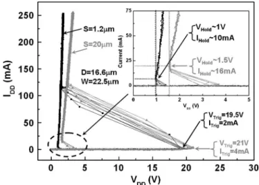
1) Latch-up DC Current–Voltage (I–V ) Characteristics of SCRStructures: The experimentally measured latch-up dc I–V characteristics of the two SCR structures with the same
D (16.6µm) and W (22.5 µm) but different values of S (1.2
and 20µm) are shown in Fig. 9. These latch-up dc I–V curves
are measured by the continuous-type curve tracer. The SCR structure withS = 1.2 µm (S = 20 µm) has a trigger voltage VTrig and a trigger current ITrigof 19.5 V (21 V) and 2 mA (4 mA), respectively. Once latch-up occurs, a low-impedance path will exist between VDD and ground to conduct a huge current.
For the same SCR, the latch-up holding voltage should be the same for both quasi-static latch-up and TLU because the holding voltage only depends on the DUT layout styles and the process parameters. However, the pull-downVDD(∼1.6 V) of the measured TLU voltage waveforms in Fig. 6(b) and (c) is somewhat higher than the holding voltage (∼1 V) in the measured latch-up dcI–V curves in Fig. 9. For the measured
TLU voltage waveforms, the pull-down VDD is equal to the
VPower−supply− (∆VResistor+ ∆VDiode). Here, VPower−supply is the applied dc voltage of the power supply, and ∆VResistor (∆VDiode) is the voltage drop across the 5-Ω current-limiting resistance (current-blocking diode). This pull-down VDD must be higher than the holding voltage of the DUT to sustain the latch-up state. For the measured latch-up dcI–V curves, however, there is neither an additional
current-limiting resistance nor a current-blocking diode, and the latch-up holding voltage is the minimum voltage that the DUT can pull down in the latch-up state. Thus, the pull-down VDD (∼1.6 V) of the measured TLU voltage waveforms is slightly higher than the holding voltage (∼1 V) in the measured latch-up dcI–V curves.
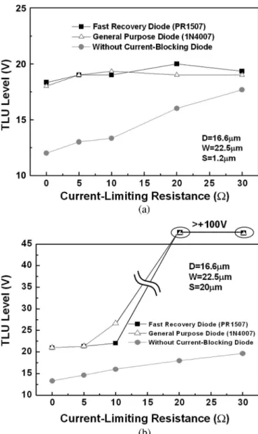
2) Positive TLU Level: For the SCR structure with layout
parameters ofD = 16.6 µm, S = 1.2 µm, and W = 22.5 µm,
the relations between the positive TLU level and current-limiting resistances under different current-blocking diodes are shown in Fig. 10(a). For the measurement setup without a current-blocking diode, the TLU level is overall smaller than that equipped with a current-blocking diode, regardless which
Fig. 9. Measured latch-up dcI–V characteristics of two SCR structures with the same D (16.6 µm) and W (22.5 µm) but different values of S (1.2 and 20µm).
diode [general purpose (1N4007) or fast recovery (PR1507)] is used. For the measurement setup with a current-blocking diode, the TLU-triggering voltage is the unipolar trigger shown in Fig. 7(c). Such unipolar trigger can generateIDsto initiate TLU whileVDDrapidly increases from+2.5 V to its positive peak voltage (i.e., largedVDD/dt). However, for the measurement setup without a current-blocking diode, the TLU-triggering voltage is the bipolar trigger shown in Fig. 7(a). Such bipolar trigger can generate ISb instead of IDs to initiate TLU while
VDDswitches from the forward-biased state(VDD< 0) to the normal reversed-biased blocking state(VDD> 0). Because ISb can initiate TLU more easily thanIDs[12], [22], the measure-ment setup without a current-blocking diode (inducedISb) can evaluate a much lower TLU level than that equipped with a current-blocking diode (inducedIDs).
The influences of the current-limiting resistance on the pos-itive TLU level are also shown in Fig. 10(a). For the measure-ment setup without a current-blocking diode, the TLU level linearly increases with the current-limiting resistance because a larger current-limiting resistance can cause a larger damping factor of the bipolar voltage onVDD, as shown in Fig. 7(b). A larger damping factor will lead to a smallerISbdue to a smaller voltage magnitude of −VPeak [22]. Therefore, although the current-limiting resistance can avoid EOS damage to the DUT, it overestimates the TLU level under a bipolar trigger voltage. However, for the measurement setup equipped with a current-blocking diode, the TLU level is almost independent of the current-limiting resistance because the current-limiting resis-tance does not obviously affectIDs[i.e.,dVDD/dt in Fig. 7(c)]. The equivalent large resistance of the current-blocking diode in series with a small current-limiting resistance(< 30 Ω) makes the effect of the current-limiting resistance negligible.
In Fig. 10(a), the TLU levels are different from the latch-up trigger voltage (+19.5 V) of the quasi-static latch-up surements shown in Fig. 9. For the quasi-static latch-up mea-surements, the main latch-up-triggering current is the reverse junction breakdown current [23]. For the TLU measurements, if the unipolar trigger is the TLU-triggering voltage, it can generate the additionalIDs (due to largedVDD/dt) to initiate
Fig. 10. Relations between the positive TLU level and current-limiting resistances under different current-blocking diodes. The SCR structure has layout parameters of (a)D = 16.6 µm, S = 1.2 µm, and W = 22.5 µm, and (b)D = 16.6 µm, S = 20 µm, and W = 22.5 µm.
TLU, in addition to the junction breakdown current. Thus, if there is a current-blocking diode (inducing unipolar trigger) and no current-limiting resistance in the TLU measurement setup, the TLU level (∼ +16 V) is slightly lower than the latch-up trigger voltage (+19.5 V) of the quasi-static latch-up measurements. However, if the bipolar trigger voltage is the TLU-triggering voltage, the major TLU-triggering current is
ISb (due to VDD switching from negative to positive voltage level) and notIDs. It has been clarified that the bipolar trigger can initiate TLU more easily than the unipolar trigger [12], [22]. Thus, there will be a much lower TLU level (∼ +12 V) if there is neither a current-blocking diode (induced bipolar trigger) nor a current-limiting resistance in the TLU measurement setup.
For the SCR structure with layout parameters of D =
16.6µm, S = 20 µm, and W = 22.5 µm, the relations between
the positive TLU level and current-limiting resistances under different current-blocking diodes are shown in Fig. 10(b). For the measurement setup equipped with a current-blocking diode,
Fig. 11. Measured VDD and IDD transient waveforms with a positive
VChargeof+35 V. A current-blocking diode (PR1507) and a current-limiting resistance of 20Ω are used in the TLU measurement setup.
the TLU level greatly increases to exceed +100 V when the current-limiting resistance is larger than 20 Ω. In fact, TLU does not occur in these cases due to one of the following two reasons: First, a larger current-limiting resistance leads the
IDD lower than the latch-up holding current. Second, a larger voltage drop across a larger current-limiting resistance makes
VDDlower than the latch-up holding voltage. No matter which one happens, TLU does not occur. For example, with a positive
VChargeof+35 V, the measured VDDandIDDtransient wave-forms under the measurement setup with a current-blocking diode (PR1507) and a current-limiting resistance of 20 Ω are shown in Fig. 11. TLU initially occurs but finally fails to be maintained because VDD is pulled down to about 1 V, which is lower than its latch-up holding voltage (∼1.5 V). Thus, an additional voltage drop across the current-blocking diode or a larger current-limiting resistance can prohibit the occurrence of TLU when the SCR has a larger latch-up holding voltage or current (D = 16.6 µm, S = 20 µm, and W = 22.5 µm).
3) Negative TLU Level: For the SCR structure with layout
parameters ofD = 16.6 µm, W = 22.5 µm, and S = 1.2 µm
(20 µm), the relations between the negative TLU level and
current-limiting resistances under different current-blocking diodes are shown in Fig. 12(a) [Fig. 12(b)]. Compared with the positive-TLU-level tests in Fig. 10(a) [Fig. 10(b)], the magnitudes of the negative TLU level are overall lower than those of the positive TLU level. For example, the magnitudes of the negative TLU level are all lower than 6 V in Fig. 12(a), but those of the positive TLU level are all higher than 10 V in Fig. 10(a). Compared with the negative-going(VCharge< 0) bipolar trigger, the positive-going(VCharge> 0) bipolar trigger needs to take an additional half-duration for decaying before
VDDreaches−VPeak. Thus, under the same voltage magnitude of both positive and negativeVCharge, the negativeVChargecan provide a larger voltage magnitude of−VPeak(i.e., largerISb) than the positiveVCharge[22]. As a result, SCR structures are more sensitive to TLU with a negative VCharge, leading to a very low negative TLU level in comparison with the positive TLU level.
Fig. 12. Relations between the negative TLU level and current-limiting resistances under different current-blocking diodes. The SCR structure has layout parameters of (a)D = 16.6 µm, S = 1.2 µm, and W = 22.5 µm, and (b)D = 16.6 µm, S = 20 µm, and W = 22.5 µm.
V. TLU SIMULATION
A 2-D device simulation tool (MEDICI) is used to verify the dependences of both the blocking diode and the current-limiting resistance on the TLU level of the SCR structure. A specified SCR structure with the same geometrical parameters (D = 16.6 µm and S = 1.2 µm) in the silicon is used for all
TLU device simulations, as shown in Fig. 13. With the device simulation, the 2-D boundary conditions of this specified SCR can be well defined to analyze TLU electrical characteristics such as transientI–V characteristics, 2-D current flow lines,
and electric field, carrier concentration.
A. Dependences of the Current-Blocking Diode on the TLU Level
From the measured TLU level dependences in Figs. 10 and 12, the TLU measurement setup equipped with a
current-Fig. 13. SCR structure used in a 2-D device simulation tool (MEDICI). This specified SCR structure has the same geometrical parameters (D = 16.6 µm andS = 1.2 µm) of SCR silicon test chips.
Fig. 14. SimulatedVDDandIDDtransient responses for TLU with unipolar trigger. It can simulate theVDDvoltage disturbance in Fig. 7(c) for the TLU measurement setup equipped with a current-blocking diode. TLU cannot be initiated even though+VPeakis as high as+20 V.
blocking diode (positive-going unipolar trigger) will lead to a higher TLU level (overestimation) of the DUT than that without a current-blocking diode (bipolar trigger). To demon-strate this phenomenon by device simulation, the simulated
VDD andIDD transient responses under unipolar and bipolar triggers are shown in Figs. 14 and 15, respectively. The related parameters of the unipolar trigger (bipolar trigger) such as rise time and falling rate (damping frequency and damping factor) are extracted from the corresponding measured waveforms in Fig. 7(c) [Fig. 7(a)].
Under the unipolar trigger in Fig. 14, TLU will not be initiated due to insufficient IDs because the increasing rate (≡ +VPeak− 2.5 V/rise time) of VDD is not large enough, even though +VPeak is as high as +20 V. Thus, IDD only comes from the small IDs or leakage current whose positive peak current IPeak is only 0.18 mA/µm; then, IDD decreases to 0 A whenVDDfinally returns to its normal operating voltage (+2.5 V). The simulated 2-D current flow line after applying the unipolar trigger voltage on VDD (at 18 ms) is also shown in the inset of Fig. 14. Clearly, TLU does not occur because no current flow line conducts through the low-impedance latch-up path between the N+ and P+ diffusions that is illustrated in Fig. 13.
Under the bipolar trigger in Fig. 15, TLU can be initiated (IDDsignificantly increases) by a large-enoughISbwhileVDD returns from−VPeak (−5 V) to the normal operating voltage
Fig. 15. SimulatedVDDandIDDtransient responses for TLU with bipolar trigger. It can simulate theVDDvoltage disturbance in Fig. 7(a) for the TLU measurement setup without a current-blocking diode. TLU can be initiated even though+VPeakis as low as+13 V.
(+2.5 V), even though its +VPeakis only+13 V, which is much smaller than the +20 V in Fig. 14 (unipolar trigger). Thus,
IDDwill be kept at a high current latch-up state (150 mA/µm) after VDD finally returns to its normal operating voltage (+2.5 V). The simulated 2-D current flow line after applying the bipolar trigger voltage onVDD (at 1200 ns) is also shown in the inset of Fig. 15. Clearly, TLU occurs because all current flow lines conduct through the low-impedance latch-up path. The simulation results in Fig. 15 are consistent with the mea-sured TLU waveforms in Fig. 6(c), whichIDDsimultaneously increases with VDD, while VDD increases from −VPeak to +2.5 V (induced ISb) but not initially from+2.5 V to +VPeak (inducedIDs). Thus,ISb is the major TLU-triggering current rather thanIDs.
TLU can also be initiated by unipolar trigger with a large-enoughIDs. For the unipolar trigger with a higher+VPeak of +25 V, the simulated VDD and IDD transient responses for TLU are shown in Fig. 16. Due to a larger increasing rate of
VDD, TLU can be initiated by a large-enough IDs whileVDD rapidly increases from the normal operating voltage (+2.5 V) to +VPeak(+25 V). Thus, IDDwill be kept at a high current latch-up state (150 mA/µm) after VDDfinally returns to its normal operating voltage.
The comprehensive simulation results in Figs. 14–16 are all consistent with the experimental results, pointing out that the TLU measurement setup equipped with a current-blocking diode will lead to a higher TLU level (overestimation) of the DUT than that without a current-blocking diode.
B. Dependences of the Current-Limiting Resistance on the TLU Level
From the measured TLU level dependences shown in Figs. 10 and 12, the TLU level of the CMOS IC (SCR) increases with the current-limiting resistance. To demonstrate this phe-nomenon by device simulation, two different bipolar triggers are used. As shown in Figs. 15 and 17, these two different bipolar triggers have the same damping frequency of∼10 MHz but different damping factors. Compared to Fig. 15, the bipolar
Fig. 16. SimulatedVDDandIDDtransient responses for TLU with unipolar trigger.VDDhas a+VPeakof+25 V, which is larger than the +20 V in Fig. 14, so the increasing rate(≡ +VPeak− 2.5 V/rise time) of VDDis large enough to produce a largeIDsto initiate TLU.
Fig. 17. SimulatedVDDandIDDtransient responses for TLU with bipolar trigger. Compared with Fig. 15, it can simulate the bipolar trigger with a larger damping factor in Fig. 7(b) for the TLU measurement setup equipped with a current-limiting resistance. TLU cannot be initiated due to insufficientISb.
trigger with a larger damping factor in Fig. 17 is used to simulate the TLU measurement setup equipped with a current-limiting resistance because the measured VDD waveforms in Fig. 7(a) and (b) show that the current-limiting resistance will lead to a larger damping factor. Clearly, because the magnitude of -VPeak decreases from 5 (Fig. 15) to 2.5 V (Fig. 17) due to a larger damping factor,ISb is not large enough to initiate TLU while VDD returns from−VPeak to its normal operating voltage. Thus, IDD does not significantly increase (IPeak is only 75µA/µm) with VDD; then,IDDdecreases to 0 A when
VDD finally returns to its normal operating voltage. Thus, the simulation results in Figs. 15 and 17 are all consistent with the experimental results, verifying that the TLU level is increased by the current-limiting resistance, as shown in Figs. 10 and 12.
VI. SUGGESTEDCOMPONENT-LEVEL
TLU MEASUREMENTSETUP
From the comprehensive measured and simulated TLU-level dependence on the current-limiting resistance and
current-blocking diode in the component-level TLU measure-ment setup, the TLU measuremeasure-ment setup without a current-blocking diode but with the small current-limiting resistance (5 Ω) is suggested. This suggested measurement setup not only can accurately evaluate the TLU immunity of CMOS ICs without overestimation but also can avoid EOS damage to the DUT during the TLU test.
The current-blocking diode should be eliminated from the TLU measurement setup to accurately evaluate the TLU immu-nity of CMOS ICs without overestimation. The bipolar transient noises on the power pins of the DUT are indeed represen-tative of the practical system-level ESD events, as shown in Figs. 2 and 3. However, because the current-blocking diode inherently alters the power supply network impedance, the use of the current-blocking diode certainly prohibits such bipolar trigger voltage on the power pins of the DUT. Instead, a unipo-lar overdamped trigger voltage will be formed if the diode was added in the TLU measurement setup. Thus, to accurately sim-ulate the practical system-level ESD event, the current-blocking diode should be eliminated from the TLU measurement setup. Additionally, the unipolar and bipolar transientVDDnoises can generate two different TLU-triggering currents, namely 1)IDs for the unipolar trigger and 2)ISbfor the bipolar trigger. It has been clarified that the bipolar trigger(ISb) can initiate TLU more easily than the unipolar trigger(IDs). Thus, to accurately represent the actual TLU immunity of the DUT under the system-level ESD test, the component-level TLU test should be performed without a current-blocking diode.
Similar to the current-blocking diode, the current-limiting resistance is also unsuitable to be equipped in the component-level TLU measurement setup. Although using the current-limiting resistance will not lead to a unipolar trigger, it certainly attenuates the voltage magnitude of the bipolar trigger (i.e., larger damping factor), as shown in Figs. 7(b) and 8(b). A larger damping factor will lead to a smaller TLU-triggering current (ISb) due to a smaller voltage magnitude of −VPeak [22]. Thus, the TLU level of the DUT will increase with the current-limiting resistance, leading to an overestimation of the TLU immunity. Even worse, a too-large current-limiting resistance (> 20 Ω) has been proven to lead TLU that does not occur in the SCR structure with a higher holding voltage (1.5 V), i.e., the SCR with a larger S of 20 µm shown in
Figs. 10(b) and 12(b). As a result, to accurately represent the actual TLU immunity of the DUT under the system-level ESD test, a small current-limiting resistance (5 Ω) is sug-gested to be used. This small current-limiting resistance has the advantage of not leading to a serious overestimation of the TLU level, as shown in Figs. 10 and 12. In addition, it can prevent the DUT from EOS damage during the high-current latch-up state.
VII. TLU VERIFICATION ONREALCIRCUITS
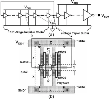
A 100-MHz ring oscillator consisting of a 101-stage inverter chain and a seven-stage taper buffer fabricated in 0.25-µm
CMOS technology is used as a real circuit for TLU verifica-tion. The schematic diagram and layout top view of the ring oscillator are shown in Fig. 18(a) and (b), respectively. The
Fig. 18. (a) Schematic diagram and (b) layout top view of the ring oscillator. The geometrical parameters X, Y, and Z represent the distances between the well edge and the well (substrate) contact, the source (drain) regions of PMOS and NMOS, and the adjacent well (substrate) contacts, respectively.
geometrical parameters X, Y, and Z represent the distances between the well edge and the well (substrate) contact, the source (drain) regions of PMOS and NMOS, and the adjacent well (substrate) contacts, respectively. The ring oscillator is treated as the DUT, where the n+ well contact and the p+ source of PMOS are connected together toVDD1, and the p+ substrate contact and the n+ source of NMOS are connected to ground. To evaluate the TLU level of the inverter chain but not that of the taper buffer, the power line of the taper buffer
VDD2 is separated from the power line of the inverter chain
VDD1. Once TLU is triggered on by a positive or negative
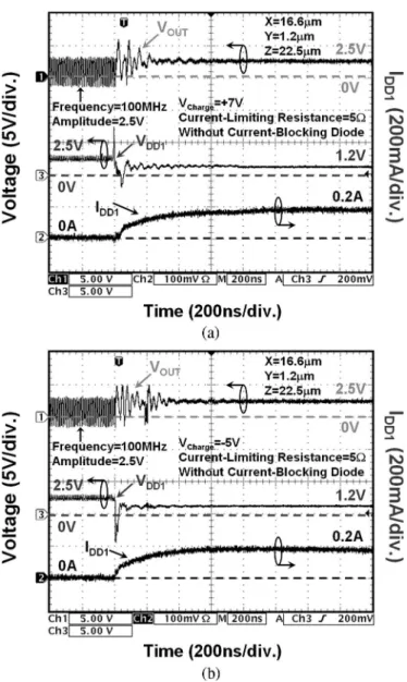
VChargewithin the ring oscillator, a rapidly increasing current will conduct through a low-impedance path betweenVDD1and ground to probably burn out the chip. To verify the TLU issue on the ring oscillator, the TLU measurement setup equipped with a current-limiting resistance of 5Ω but without a current-blocking diode is used. For the ring oscillator with layout parameters ofX = 16.6 µm, Y = 1.2 µm, and Z = 22.5 µm,
the measured VDD1, IDD1, andVOUT transient responses for TLU withVCharges of+7 and −5 V are shown in Fig. 19(a) and (b), respectively. In both cases, TLU is triggered on due to a large-enoughISbwhileVDD1increases from its negative peak voltage to the normal operating voltage (+2.5 V). Meanwhile, the rapidly increasingIDD1 accompanies the pull-downVDD1 due to a low-impedance path betweenVDD1and ground. Thus, the ring oscillator fails to function correctly, causing the output voltage of the ring oscillator VRing to be pulled down to ground. Thus, VOUT is kept at+2.5 V after the seven-stage taper buffer.
Four measurement setups with two different types of current-blocking diodes (PR1507 and 1N4007) and current-limiting resistances (5 and 20 Ω) are used to verify whether the sug-gested measurement setup has the lowest TLU level (without overestimation). Moreover, ring oscillators with two sets of
Fig. 19. MeasuredVDD1,IDD1, andVOUTtransient waveforms of the ring oscillator with aVChargeof (a)+7 and (b) −5 V. The TLU measurement setup with a current-limiting resistance of 5Ω but without a current-blocking diode.
layout parameters (X = 16.6, Y = 1.2, and Z = 22.5 µm, and X = 16.6, Y = 10, and Z = 0.3 µm) are also used to
inves-tigate the layout dependences on the TLU level. Table I lists the TLU levels of the ring oscillators with two sets of layout parameters under four different TLU measurement setups.
For the ring oscillator with layout parameters ofX = 16.6, Y = 1.2, and Z = 22.5 µm, both the positive and negative
TLU levels measured by the suggested TLU measurement setup (type A) are lower than those measured by the other three measurement setups (types B, C, and D) where a current-blocking diode or a large current-limiting resistance of 20 Ω is used. For the ring oscillator with layout parameters of
X = 16.6 µm, Y = 10 µm, and Z = 0.3 µm, TLU occurs
only for the suggested measurement setup (type A). In the other measurement setups (types B, C, and D), the additional voltage drop across the current-blocking diode or the large current-limiting resistance leads the VDD (IDD) lower than the holding voltage (holding current) of the parasitic SCR in
the ring oscillator. Thus, it has been proven once again that the suggested measurement setup (no current-blocking diode but a small current-limiting resistance) can efficiently evaluate the TLU level of CMOS ICs without overestimation.
VIII. CONCLUSION
An efficient component-level TLU measurement setup with bipolar trigger, which can accurately evaluate (without over-estimation) the TLU immunity of CMOS ICs under the system-level ESD test for EMC regulation, has been proposed and successfully verified with silicon test chips and device simulation. Through investigating the influences of both the current-blocking diode and current-limiting resistance on the TLU-triggering voltage waveform and TLU level, it has been demonstrated that the TLU measurement setup equipped with either a current-blocking diode or a current-limiting resistance will overestimate the TLU level of CMOS ICs. However, a small current-limiting resistance has no significant impact to the TLU level; therefore, the TLU measurement setup without a current-blocking diode but with a small current-limiting re-sistance of 5Ω is suggested. This suggested TLU measurement setup not only can accurately evaluate the TLU immunity of CMOS ICs without overestimation but also can avoid EOS damage to the DUT during the TLU test. Such TLU measure-ment setup can be widely utilized to evaluate the TLU immunity of CMOS ICs in practical field applications.
ACKNOWLEDGMENT
The authors would like to thank Dr. C.-C. Tasi, Dr. T.-Y. Chen, and Mr. W.-Y. Lo for their valuable technical discussions.
REFERENCES
[1] S. Voldman, “Latch-up—It’s back,” in Threshold Newsletter. Rome, NY: ESD Association, Sep./Oct. 2003.
[2] J. T. Mechler, C. Brennan, J. Massucco, R. Rossi, and L. Wissel, “Contention-induced latchup,” in Proc. IRPS, 2004, pp. 126–129. [3] K. Domanski, S. Bargstätd-Franke, W. Stadler, M. Streibl, G. Steckert,
investigation and computer aided simulations,” in Proc. IRPS, 2004, pp. 370–374.
[4] K. Chatty, P. Cottrell, R. Gauthier, M. Muhammad, F. Stellari, A. Weger, P. Song, and M. McManus, “Model-based guidelines to suppress cable discharge event (CDE) induced latchup in CMOS ICs,” in Proc. IRPS, 2004, pp. 130–134.
[5] K. Domanski, S. Bargstätd-Franke, W. Stadler, U. Glaser, and W. Bala, “Development strategy for TLU-robust products,” in Proc. EOS/ESD
Symp., 2004, pp. 299–307.
[6] G. Boselli, V. Reddy, and C. Duvvury, “Latch-up in 65 nm CMOS tech-nology: A scaling perspective,” in Proc. IRPS, 2005, pp. 137–144. [7] S. Voldman, “Latchup and the domino effect,” in Proc. IRPS, 2005,
pp. 145–156.
[8] M.-D. Ker and Y.-Y. Sung, “Hardware/firmware co-design in an 8-bit microcontroller to solve the system-level ESD issue on keyboard,” in
Proc. EOS/ESD Symp., 1999, pp. 352–360.
[9] M.-D. Ker and S.-F. Hsu, “Evaluations on board-level noise filter networks to suppress transient-induced latchup under system-level ESD test,” in
Proc. EOS/ESD Symp., 2005, pp. 262–269.
[10] M. Kelly, L. Henry, J. Barth, G. Weiss, M. Chaine, H. Gieser, D. Bonfert, T. Meuse, V. Gross, C. Hatchard, and I. Morgan, “Developing a tran-sient induced latch-up standard for testing integrated circuits,” in Proc.
EOS/ESD Symp., 1999, pp. 178–189.
[11] I. Morgan, C. Hatchard, and M. Mahanpour, “Transient latch-up using an improved bi-polar trigger,” in Proc. EOS/ESD Symp., 1999, pp. 190–202.
[12] M.-D. Ker and S.-F. Hsu, “Evaluation on efficient measurement setup for transient-induced latchup with bi-polar trigger,” in Proc. IRPS, 2005, pp. 121–128.
[13] E. Hamdy and A. Mohsen, “Characterization and modeling of transient latchup in CMOS technology,” in IEDM Tech. Dig., 1983, pp. 172–175. [14] S. Bargstätd-Franke, W. Stadler, K. Esmark, M. Streibl, K. Domanski,
H. Gieser, H. Wolf, and W. Bala, “Transient latch-up: experimental analy-sis and device simulation,” in Proc. EOS/ESD Symp., 2003, pp. 70–78. [15] Transient Latch-up Testing—Component Level Supply Transient
Stim-ulation, ESD Association Standard Practice, ANSI/ESD SP5.4-2004,
2004.
[16] R. R. Troutman and H. P. Zappe, “A transient analysis of latchup in bulk CMOS,” IEEE Trans. Electron Devices, vol. ED-30, no. 2, pp. 170–179, Feb. 1983.
[17] EMC—Part 4–2: Testing and Measurement Techniques—Electrostatic
Discharge Immunity Test, IEC 61000-4-2 International Standard,
2001.
[18] M.-D. Ker and S.-F. Hsu, “Transient-induced latchup in CMOS technol-ogy: Physical mechanism and device simulation,” in IEDM Tech. Dig., 2004, pp. 937–940.
[19] ——, “Physical mechanism and device simulation on transient-induced latchup in CMOS ICs under system-level ESD test,” IEEE Trans. Electron
Devices, vol. 52, no. 8, pp. 1821–1831, Aug. 2005.
[20] IC Latch-up Test, EIA/JEDEC Std. no. 78, 1997.
[21] Electrostatic Discharge (ESD) Sensitivity Testing—Machine Model (MM), EIA/JEDEC Standard Test Method A115-A, 1997.
[22] S.-F. Hsu and M.-D. Ker, “Dependences of damping frequency and damping factor of bi-polar trigger waveforms on transient-induced latchup,” in Proc. EOS/ESD Symp., 2005, pp. 118–125.
[23] R. Troutman, Latch-up in CMOS Technology: The Problem and the Cure. New York: Kluwer, 1986.
Ming-Dou Ker (S’92–M’94–SM’97) received the
B.S., M.S., and Ph.D. degrees from the National Chiao-Tung University (NCTU), Hsinchu, Taiwan, R.O.C., in 1986, 1988, and 1993, respectively.
He was a Circuit Design Engineer at the VLSI Design Department, Computer and Communication Research Laboratories, Industrial Technology Re-search Institute (ITRI), Taiwan, R.O.C., in 1994, and was promoted to Department Manager in 1998. He is currently a Full Professor at the Department of Electronics Engineering, NCTU. He had been invited to teach/provide consultation sessions on the reliability and quality design of integrated circuits by hundreds of design houses and semiconductor companies at the Science-Based Industrial Park, Hsinchu, in Silicon Valley, San Jose, CA, in Singapore, and in mainland China. He has proposed many inventions to improve the reliability and quality of integrated circuits, which were granted 113 U.S. patents and 123 Taiwan, R.O.C. patents. He has published over 270 technical papers in international journals and conferences in the field of reliability and quality design for CMOS integrated circuits. His current research interests include reliability and quality design for nanoelectronics and gigascale systems, high-speed and mixed-voltage input/output interface circuits, especially sensor circuits, and on-glass circuits for system-on-panel applications in thin-film transistor liquid-crystal display.
Dr. Ker has served as a member of the Technical Program Committee and the Session Chair of numerous international conferences (including IEEE ISCAS, IEEE AP-ASIC, IEEE SOC, IEEE IRPS, IEEE ISQED, IPFA, EOS/ESD Symposium, IEEE VLSI-TSA, etc.). He was elected as the first President of the Taiwan ESD Association in 2001. He also served as the Technical Program Committee Chair of the 2002 Taiwan ESD Conference, the General Chair of the 2003 Taiwan ESD Conference, the Publication Chair of the 2004 IPFA, and the ESD Program Chair of the 2004 International Conference on Electromagnetic Applications and Compatibility. He has served as the Chair of the RF ESD committee of the 2004 International EOS/ESD Symposium, the Vice-Chair of the Latch-up committee of the 2005 IEEE International Reliability and Physics Symposium, the Organizer of the Special Session on ESD Protection Design for Nanoelectronics and Gigascale Systems in ISCAS’05, and the Chair of the TRD track of the 2006 IEEE International Symposium on Quality Electronic Design. He currently serves as the Associate Editor of the IEEE TRANSACTIONS ON
VLSI SYSTEMS. He was the recipient of many research awards from ITRI, the National Science Council, and the NCTU, and received the Dragon Thesis Award from Acer Foundation. In 2003, he was selected as one of the Ten Outstanding Young Persons in Taiwan by Junior Chamber International. In 2005, one of his patents on ESD protection design has been awarded with the National Invention Award in Taiwan.
Sheng-Fu Hsu (S’04) received the B.S. degree
from the Department of Engineering and System Science, National Tsing-Hua University, Hsinchu, Taiwan, R.O.C., in 2000, and the M.S. and Ph.D. degrees from the Institute of Electronics, National Chiao-Tung University, Hsinchu, in 2002 and 2006, respectively.
His current research interests include semicon-ductor device physics and IC reliability.
![Fig. 1. Measurement setup of the system-level ESD test with indirect contact- contact-discharge test mode [17]](https://thumb-ap.123doks.com/thumbv2/9libinfo/7527947.119511/1.891.454.821.291.549/fig-measurement-setup-level-indirect-contact-contact-discharge.webp)