A 1.2-V 5.2-mW 20–30-GHz Wideband
Receiver Front-End in 0.18- m CMOS
Chun-Hsing Li, Student Member, IEEE, Chien-Nan Kuo, Member, IEEE, and Ming-Ching Kuo, Member, IEEE
Abstract—This paper presents a low-power wideband receiver front-end design using a resonator coupling technique. Induc-tively coupled resonators, composed of an on-chip transformer and parasitic capacitances from a low-noise amplifier, a mixer, and the transformer itself, not only provide wideband signal transfer, but also realize wideband high-to-low impedance transformation. The coupled resonators also function as a wideband balun to give single-to-differential conversion. Analytic expressions for the coupled resonators with asymmetric loads are presented for design guidelines. The proposed receiver front-end only needs a few passive components so that gain degradation caused by the passive loss is minimized. Hence, power consumption and chip area can be greatly reduced. The chip is implemented in 0.18- m CMOS technology. The experimental result shows that the 3-dB bandwidth can span from 20 to 30 GHz with a peak conversion gain of 18.7 dB. The measured input return loss and third-order intercept point are better than 16.7 dB and 7.6 dBm, respec-tively, over the bandwidth. The minimum noise figure is 7.1 dB. The power consumption is only 5.2 mW from a 1.2-V supply. The chip area is only 0.18 mm .
Index Terms—CMOS, common-gate (CG) low-noise amplifier (LNA), inductively coupled resonators (ICRs), low power, low voltage, mixer, resonator coupling network (RCN), wideband.
I. INTRODUCTION
T
HE applications within the - and -band have ig-nited intensive research activities. There exist systems of 22–29-GHz short-range radar, 24-GHz industrial–scien-tific–medical (ISM) band, and local multipoint distribution services (LMDS) [1]–[4]. A wideband receiver is thus prefer-able to a narrowband one for versatile functions. However, designing a receiver to cover such a wide and high frequency band is challenging because of lossy passive components and low transistor speed. For example, 0.18- m CMOS technology offers the unity current gain frequency only around 55 GHz. More advanced CMOS technology can be adopted to provide Manuscript received April 12, 2012; revised August 19, 2012; accepted Au-gust 22, 2012. Date of publication September 17, 2012; date of current version October 29, 2012. This work was supported by the National Science Council, Taiwan, under Grant NSC 009-013 and Grant NSC 100-2220-E-009-056, by the Ministry of Education in Taiwan under the Aiming for the Top University (ATU) Program, and by MediaTek Inc. under a fellowship.C.-H. Li and C.-N. Kuo are with the Department of Electronics Engineering and the Institute of Electronics, National Chiao Tung University, Hsinchu 300, Taiwan (e-mail: [email protected]; [email protected]).
M.-C. Kuo is with the Information and Communications Research Labora-tories (ICL), Division for Biomedical and Industrial Integrated Circuit Tech-nology, Industrial Technology Research Institute (ITRI), Hsinchu 310, Taiwan (e-mail: [email protected]).
Color versions of one or more of the figures in this paper are available online at http://ieeexplore.ieee.org.
Digital Object Identifier 10.1109/TMTT.2012.2216285
higher speed transistors, but with higher cost. Moreover, the supply voltage shrinks with the technology, making the CMOS design more challenging. Hence, appropriate circuit topologies are required to provide wideband operation using as few pas-sive components as possible, while consuming low power in low voltage.
Many prior studies were proposed for - and -band ap-plications. Only a few belong to true wideband operation in sil-icon-based technologies of CMOS and BiCMOS. A 22–29-GHz ultra-wideband (UWB) pulse-radar receiver in 0.18- m CMOS was proposed using a multistage low-noise amplifier (LNA) with the neutralization technique [1]. However, the pro-posed circuit requires many inductors, resulting in large area. A receiver front-end using a two-stage LNA and microstrip lines is shown to work from 21 to 29 GHz [5]. Nevertheless, the front-end is bulky because it uses area-consuming transmis-sion lines for impedance matching. A dual-band 24/31-GHz re-ceiver is presented by combining a wideband two-stage LNA and a wideband mixer in a 0.18- m BiCMOS process [6]–[8]. The reported circuit adopts a single-balanced mixer. Hence, LO leakages might desensitize the following stages. A wideband LNA was reported using resistive feedback to work well in the -band [9]. It still requires a wideband mixer and a wideband balun to realize a wideband receiver.
The architectures of the aforementioned circuits demand mul-tistage amplifiers to tackle the low issue. Many inductors or transmission lines are necessary to sustain a wideband response. However, utilizing a large number of passive components not only introduces high signal loss, but also occupies large chip area. Power consumption is inevitably increased to compensate the loss for enough gain. Consequently, proper circuit topolo-gies should be developed to give wideband operation while dis-sipating low power and featuring a small form factor.
Using the technique of resonator coupling is a promising al-ternative for wideband operation. Recently, the resonator cou-pling technique is widely exploited to increase the transmission distance in the wireless power transfer application [10]–[13]. It is also applied to circuits for wireless communication sys-tems, such as a narrowband receiver front-end [14], a wideband LNA design [7], an output load of the mixer [15], a low-power narrowband down-conversion mixer [16], a wideband multi-mode voltage-controlled oscillator (VCO) [17], and a low noise quadrature VCO [18]. Circuit design, however, is usually as-sumed to be under a symmetric load condition, which is not nec-essarily true in many realistic circuit implementations. Further-more, few physical insights on wideband operations are given.
In this paper, a compact 20–30-GHz receiver front-end is de-signed by using a resonator coupling network (RCN) placed be-tween the LNA and the mixer to realize inter-stage matching. It 0018-9480/$31.00 © 2012 IEEE
only requires two coupled resonators to support wideband oper-ation. The coupled resonators form a high-order filter to perform functions of a wideband load and wideband impedance transfor-mation simultaneously. Moreover, they act as a wideband balun without paying additional power in realizing single-to-differen-tial conversion. All of the design effort enables the receiver to be realized with a small form factor and low power consump-tion.
The RCN with an asymmetric load condition is analyzed in detail to provide design guidelines. Analytic formulas for the critical coupling condition, passive gain, peak gain frequency separation (FS), and Ripple are presented. In contrast to the con-ventional coupled-resonator filter design that is commonly ap-plied for narrowband operation [19], the proposed methodology can be adopted for wideband design with a simple and insightful design process. This paper is organized as follows. Section II details the theory of the inductively coupled resonators (ICRs), including the proposed design flow. In Section III, the con-sideration of the receiver architecture and the design of each building block are presented. The experimental result is shown in Section IV. Finally, Section V concludes this study.
II. THEORY OFICRs
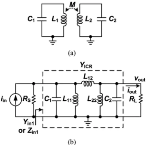
An RCN is employed to transfer a signal, in current, voltage, or power domain, from one resonator to the other, as indicated in Fig. 1(a), in which and represent the source and load resistances, respectively. The coupling is conducted either by an inductor or a capacitor . The ICR is especially attractive since it can be realized by an on-chip transformer. This not only leads to small chip area, but also provides single-to-differential conversion without dissipating any power. The RCN is widely adopted to increase the frequency selectivity in bandpass filter design [19]. It can also provide passive gain by impedance trans-formation, which is particularly attractive to low-power appli-cations [14].
The typical frequency response of the ICR exhibits resonance frequencies of two oscillatory modes at and , as illus-trated in Fig. 1(b). If the critical coupling condition is met, the gain levels at and are maximum and equal. This implies that the impedance is matched concurrently at and for both the input and output ports. The peak-to-peak variation, i.e., Ripple, is defined as
Ripple (1)
where is the maximum gain and is the minimum gain at the frequency of . If Ripple is less than 3 dB, the ICR response can be considered as wideband.
In this study, the design goal is therefore to make the critical coupling condition occur at two widely separated and simultaneously, and keep Ripple within 3 dB. Although only the ICR case is considered as follows, the same approach can also apply to the capacitively coupled resonators.
A. ICR Without Loading Effect
Fig. 2(a) shows the ICR circuit of double resonance. One res-onator, and , is coupled to the other, and , mag-netically. Without loss of generality, the transformer is assumed
Fig. 1. (a) RCN. The network is coupled either inductively or capacitively. (b) Typical frequency response of the RCN. Gain can be current, voltage, or power gain. is the radian frequency.
Fig. 2. (a) Network of ICRs. (b) Equivalent circuit of the coupled resonators as the transformer is replaced by its -model.
lossless. The coupling coefficient is defined by the mutual in-ductance between the two coils as [14]
(2) Let the resonance frequencies of the uncoupled resonators be defined, respectively, as and with the frequency ratio
of [14].
Taking the mutual coupling effect into account, the natural resonance frequencies of the coupled network change. They can be derived in terms of , , and , as and [14]. The governing equation of the resonance frequencies is established as
(3) Consider the coupled resonators in a circuit to analyze signal transfer, as shown in Fig. 2(b). The transformer is replaced with
its -model equivalent circuit, in which , , and is related to and [20].
The critical coupling condition occurs provided that the ICR input is impedance matched to the source, or , at and [14]. It leads to
(4) where is the coil turn ratio of the transformer, defined as
(5) From (4), another governing equation of and is ob-tained as
(6) It concludes from (3), (4), and (6) that the critical coupling condition of the ICR can be acquired at both and if
(7) (8) Namely, those uncoupled resonators need to have the same resonance frequencies, i.e., , and must be equal to the impedance transformation ratio.
B. ICR With Loading Effect
Resonance occurs at the frequencies that the imaginary part of the input admittance equals to zero. The resistor load in Fig. 2(b) actually affects the resonance frequencies such that and need to be modified. The effect becomes severe especially when the loaded quality factor is low for wideband operation. Note that (7) and (8) still hold for achieving critical coupling at resonance frequencies, even with the loading effect.
The two-port admittance matrix of the ICR, , is used to derive the modified resonance frequencies in Fig. 2(b). The optimal transfer occurs when . This input admittance can be derived from the admittance matrix by
(9) Given the critical coupling condition by (7) and (8), the matrix elements of can be easily shown as
(10)
where and are defined as
(11) Essentially corresponds to the quality factor of the uncoupled loaded resonators.
Let the imaginary part of the input admittance be zero. The solution gives the modified resonance frequencies of the ICR with the loading effect. Two parallel and one series 1 resonance frequencies can therefore be found. They are
(12) (13) When is high, (12) can be simplified as
(14) As expected, (14) is the same as and when , indicating that the loading effect can be neglected.
At and , the input admittance becomes a real value, given by
(15) The impedance matching condition is achieved. The ICR can couple the signal with the highest gain. This confirms the critical coupling condition in (7) and (8), even with the loading effect. In essence, this is an impedance transformation process to meet the optimal loading condition. On the other hand, impedance transformation is different at . The input impedance is given as
(16) which fails to meet the critical coupling condition. That is, en-ergy coupling is less efficient than that at and .
Note that coincides with at as . Al-though it appears that the critical coupling condition is achieved at as , the coupling system exhibits a narrowband re-sponse, undesired for the wideband operation. It is also observed that is very close to the minimum gain frequency as is high and is small.
C. Signal Gain
The passive coupled system in Fig. 2(b) can give signal cur-rent or voltage gain, utilizing impedance transformation. This passive gain by the impedance transformation is very useful for the low power application since it does not consume any power.
1Strictly speaking, is not considered as a resonance frequency of the
cou-pling system since the highest gain is not gained at it in most case, except as as indicated in (16).
Consider all of the available power from the source is delivered to the load, i.e.,
(17) If , it yields to the maximum current gain given by
(18) If , it achieves the maximum voltage gain given by
(19) The maximum gain is obtained under the impedance matching condition.
An ideal transformer gives the maximum gain in the broadband sense. If the turn ratio is set as for the impedance transformation, the maximum current gain can be obtained over infinite bandwidth. In the case of an RCN, the maximum gain occurs only at the resonance frequencies calcu-lated by (12). Gain decreases to a minimum between the two peak gain frequencies, resulting in gain variation. It is critical to make wide separation between the peak gain frequencies, and keep Ripple less than 3 dB.
The closed form of the ICR current gain can be derived as (20) After substituting (10) into (20), the current gain can be shown as
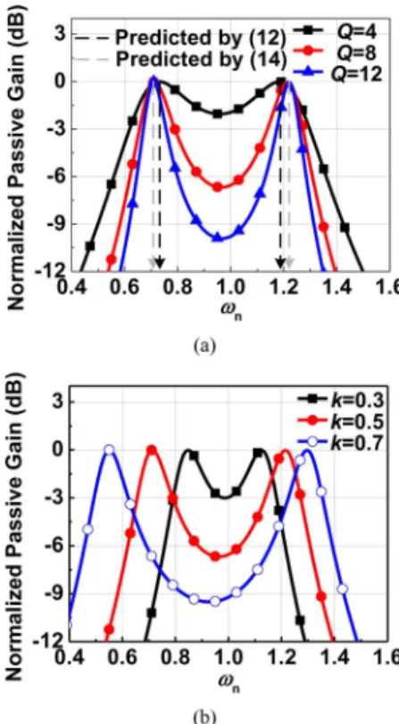
(21) where is the frequency normalized to , i.e., . The voltage gain can also be derived by transforming the Norton current source into the Thevenin voltage. Note that the derived gain formulas are exactly matched to the simulation results. It is quite cumbersome to formulate the closed form of the minimum passive gain. Instead, the results are observed numerically. The normalized current gain using (18) and (21) is plotted in Fig. 3, where and are varied.
It is clear that the minimum gain occurs at the frequency of , i.e., not equal to . By observing the gain response, is approximately at , the arithmetic average of and . From (18) and (21), Ripple can be acquired as
Ripple
(22) where . For convenience, we define a parameter of FS as
(23)
Fig. 3. Normalized passive gain versus . (a) is fixed at 0.5. (b) is fixed at 8.
Note that the actual 3-dB bandwidth is wider than (23) since and correspond to the highest gain that the RCN can pro-vide. It is evident that the resonance frequencies are affected by , the loading effect, and , the coupling. Higher FS can be obtained if the coupling is stronger, but larger Ripple is also in-troduced. On the other hand, smaller and result in smaller Ripple at the price of narrower FS. Obviously, there exists a tradeoff between FS and Ripple to meet a desired wideband re-sponse with an acceptable Ripple level. Fig. 4 shows the com-parison between simulation and calculation results of FS and Ripple as and are varied. The calculation results match well with simulation ones.
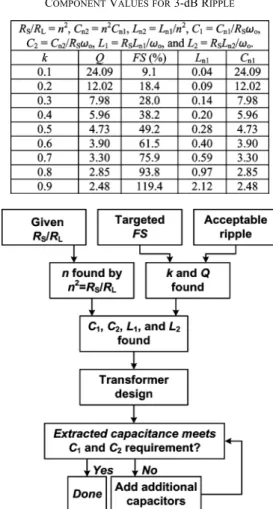
Contour plots can help designers to choose an appropriate combination of and to trade off FS and Ripple. Two plots in Fig. 5 are superposed over the range of and from 0 to 15 and 0 to 1, respectively. The No Solution region represents that the ICR no longer resonates at and , but only at . Actually, it is bounded by , corresponding to zero FS. The contour line of 3-dB Ripple is highlighted via a blue line (in the online version) with circular symbols. The associated component values are summarized in Table I. These parameters are normalized to and so that they can be easily scaled to the frequency band of interest.
D. Design Flow of the ICR
With the derived transfer functions, FS, and Ripple, the ICR for the wideband impedance transformation can be designed systematically. In the first place, the coil turn ratio is selected according to the ratio. Given the targeted FS and the acceptable Ripple, the values of and can be determined. is obtained since it locates at the center of the interested
Fig. 4. Comparison between simulation and calculation results of FS and Ripple. (a) is fixed at 0.5. (b) is fixed at 8.
Fig. 5. Contour plots of FS and Ripple versus the coupling coefficient and the quality factor of .
band. is then found from . From (11), , , , and can be determined exactly. A transformer is designed to meet the component values. Additional capacitors can be added if the extracted parasitic capacitance does not meet the requirement. The design flow of the ICR is summarized in Fig. 6.
The properties of compact chip area, wideband impedance transformation, and working as a balun make the ICR very suit-able for on-chip circuit design. Hence, the ICR is incorporated into the proposed wideband receiver front-end to realize a com-pact, low power, and low-cost solution. Section III is going to present the details of the receiver design.
TABLE I
COMPONENTVALUES FOR3-dB RIPPLE
Fig. 6. Design flow of the ICR for wideband applications.
III. WIDEBANDRECEIVERDESIGN
The receiver architecture under consideration is shown in Fig. 7 [14]. The direct-conversion architecture is adopted for the sake of a minimal number of components. It also elimi-nates the need of an image rejection filter. In this study, only the -path is implemented, including an LNA, a balun, and a double-balanced mixer. The -path can be easily incorporated by using the same design. The design needs to provide wide-band responses of voltage-to-current conversion in the LNA stage, single-to-differential conversion in the balun, and cur-rent-to-voltage frequency conversion in the mixer. Hence, poles associated with the LNA output capacitance , the mixer input capacitance , and other parasitic ones, shall be con-sidered carefully.
Fig. 8 shows the proposed wideband receiver front-end. Low power operation is feasible since it only needs a few passive components and amplifier stages. The LNA adopts a common-gate (CG) topology, which gives a wideband response not only in gain, but also in noise and linearity. It also directly works as the transconductor stage of the mixer, which is a great ben-efit in reducing power consumption [14]. The ICR fulfills the balun function and inter-stage impedance transformation. Actu-ally the two coupled resonators absorb the parasitic capacitances from the LNA, transformer, and mixer into the design, which is favorable for bandwidth enhancement of alleviating the issue
Fig. 7. Adopted direct-conversion architecture. This study includes the design of an LNA, a balun, and a mixer in the -path.
Fig. 8. Proposed wideband receiver front-end. The ICR functions as a balun and also provides wideband impedance transformation. is used as a dc blocking capacitor.
due to the mixer input pole and the LNA output pole. Finally, the double-balanced mixer provides the frequency down-con-version and eliminates LO leakages from desensitizing the fol-lowing stages [14]. The Sections III-A–III-C will detail each block design.
A. LNA Design
The LNA is a critical block to provide a wideband response, not only in input matching but also in noise figure (NF) and lin-earity. It was proposed to apply a common-source (CS) struc-ture with a high-order input matching network for wideband operation [21], [22]. However, the approach calls for a large number of inductors, requiring large chip area and increasing NF. In this study, the common-gate low-noise amplifier (CG-LNA) is instead chosen, which is in need of only one inductor. The CG-LNA is also advantageous because it has better re-verse isolation and stability [23]. The most significant feature is that it provides better noise performance for higher oper-ating frequency since the gate-induced noise is insensitive to ( is the unity current gain frequency) while the CS-LNA is proportional to [24].
The input equivalent circuit of the CG-LNA is established to analyze the input matching, as shown Fig. 9(a), in which is the source resistance and and are the gate-to-source capacitance and the transconductance of , respectively. It requires equal to for impedance matching. tunes out only at the center of the frequency band. Wideband
Fig. 9. (a) Equivalent circuit for the input matching network. (b) Equivalent circuit for the matching network at the drain.
matching relies on the low quality factor of the input matching network. The input impedance can be derived as
(24)
where and are defined as
(25) representing the quality factor and the resonance frequency of the input matching network, respectively. To have bandwidth of 0.4 , i.e., 40%, needs to be smaller than 2.5. Note that the above derivation assumes infinite output resistance . If is finite, the loading at the drain will affect the input matching. can be adjusted to move back to the desired frequency. The parasitic capacitance at the drain node of introduces a nondominant pole and degrades the LNA bandwidth. For band-width enhancement, the inductor is added to form a -net-work together with the gate-to-drain capacitance of and the gate-to-source capacitance of , as shown in Fig. 9(b). The network is driven by the output short cur-rent with the impedance of twice of the output re-sistance , and loaded by the input resistance expressed
as , where is the effective load
seen by . The network generates the output current , equal to the LNA output current through the CG tran-sistor. Smaller values present wider bandwidth of the cur-rent transfer, but with the price of larger gain ripple [25]. In this study, the network is intentionally designed to provide gain peaking around 28 GHz for the concern of higher ICR loss at
in practice.
Adding can also minimize the variation of the LNA noise within the interested band. The NF is dominated by in the low operating frequency. noise can be neglected because of high degeneration impedance at its source. However, the de-generation impedance decreases at the high operating frequency due to the parasitic pole at the drain. This causes noise contribution to rise rapidly along with the frequency. boosts
Fig. 10. Frequency response of the NF and IIP3 as either is or is included.
Fig. 11. Equivalent circuit of the ICR.
the LNA gain at and also helps suppress noise. Hence, the noise can be assumed to be mainly contributed by the transistor. Accordingly, the noise factor can be derived as
(26) where , , and are process-dependent noise parameters [26]. is dominated by the second factor associated with the channel thermal noise. The only frequency-dependent term is the third one, which has a small weighting factor, implying less sen-sitivity of the NF to the frequency variation. Actually, noise matching only occurs within a narrow frequency range since no feedback technique is employed. However, can minimize the NF variation within the interested frequency band. Fig. 10 shows the post-layout simulation results of the NF frequency response with and without . The variation becomes smaller than 0.63 dB over the 20–30-GHz band after is added.
For the linearity consideration, the CG-LNA has a superior input third-order intercept point (IIP3) as compared to the CS counterpart [27]. In general, the linearity is strongly affected by the LNA output loading [14]. That is, the IIP3 is insensitive to the frequency variation as long as the LNA faces a wideband load. In this study, the wideband load is achieved by the ICR to sustain wideband linearity performance. Fig. 10 shows the post-layout simulation results of the IIP3 with and without as the LNA is loaded with the ICR and the mixer. The IIP3 is degraded as is included. However, the IIP3 is still better than 0.6 dBm. It is worth trading off the linearity for the NF improvement.
Fig. 12. Proposed transformer. , , and are the width and spacing of the primary and secondary coils, respectively. OD is the outside dimension.
Fig. 13. EM simulation results of the proposed transformer.
Fig. 14. Post-layout simulation results of the NF and the IIP3 of the mixer.
Based on the above discussion, the bias and the transistor size can be designed accordingly. To make equal to , the transistor with higher and smaller size can be chosen or vice versa. A smaller transistor can increase the matching bandwidth, but at the price of higher power consumption and larger . On the other hand, the power consumption can be re-duced by choosing a larger transistor, but at the cost of narrower bandwidth and higher noise. To make good tradeoff among the power, NF, and chip area, the bias and the transistor size are de-signed as 0.77 V and 60 m, respectively. of 0.23 nH is em-ployed to resonate at around 25 GHz. The quality factor is cal-culated to be 1.4, corresponding to the bandwidth of 17.8 GHz. The LNA only draws 3.8 mA from a 1.2-V supply.
Fig. 15. Gain response of each building block, including the LNA, the mixer (including the ICR), and the whole receiver front-end.
Fig. 16. Chip micrograph of the proposed receiver front-end.
Fig. 17. Measured input return loss.
B. Mixer Design
The mixer is implemented in the doubled-balanced configu-ration for better port-to-port isolation. This is especially critical for the direct conversion receiver. In this study, the LNA is di-rectly utilized as the transconductor stage to reduce the power consumption. Since the mixer linearity is mainly bounded by the transconductor stage, the CG-LNA also benefits in mixer performance due to the degeneration resistance .
– transistors act as the switching stage. pMOS transistors are chosen because of better flicker noise performance. Ideally, only one switching path is on at a time. Nonideal switching, however, degrades the noise and the gain performance. To re-duce the time interval in which the switching transistors are on simultaneously, local oscillator (LO) power of 1 dBm and
Fig. 18. Measured RF bandwidth.
Fig. 19. Measured IIP3.
Fig. 20. Measured NF.
– of 0.49 V, near the transistor threshold voltage, are chosen. and are designed as 2 k and 0.3 pF, resulting in IF bandwidth around 300 MHz.
C. ICR Design
Once the design of the mixer and the LNA is completed, the ICR is employed to provide wideband signal transfer. Fig. 11 illustrates the equivalent-circuit model [14]. The output and the input impedances of the LNA and the mixer are modeled by
, , , and , respectively. , ,
, and model the parasitic capacitances and the ohmic losses of the transformer, respectively. To ease the analysis, the transformer is assumed lossless. Since the transformer is sym-metric to the virtual ground of the secondary coil, the ICR can
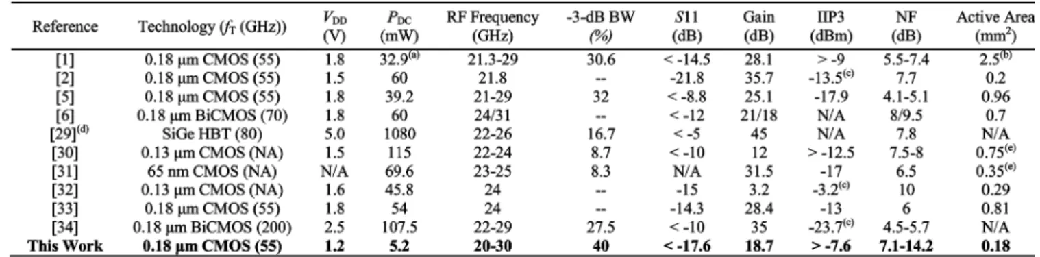
TABLE II
PERFORMANCESUMMARY ANDCOMPARISONWITHPRIORSTUDIES
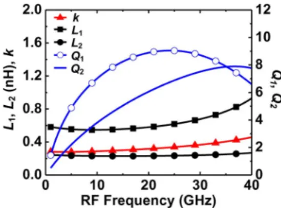
be analyzed by using the upper half circuit of Fig. 11. As com-pared to Fig. 2, the developed ICR theory can be applied di-rectly here. Following the design flow in Fig. 6, the ICR can be designed systematically. In the first place, the coil turn ratio is selected as 1.5 due to the ratio. The targeted FS and the Ripple are around 30% and 3 dB, respectively. From Table I, of around 8 and of 0.3 are chosen. is located at 25 GHz, the center of the interested band. is then found to be 25.34 GHz. of 72 fF, of 163 fF, of 0.6 nH, and of 0.27 nH, are determined accordingly.
The designed transformer is shown in Fig. 12, where the port is connected to the LNA, and the and ports are con-nected to the double-balanced mixer. The width of the primary and secondary coils, and , is chosen as 8 m. The spacing is designed as 6 m to let near the desired value of 0.3. The outside dimension OD is chosen as 130 m to fulfill the and requirement. The electromagnetic (EM) simulation results of the proposed transformer are illustrated in Fig. 13. The ex-tracted transformer parameters are , , , , , and of 0.59 nH, 0.24 nH and 1.6, 0.28, 2.48, and 3 , respectively. Note that , , and are extracted at low-frequency range as the capacitive effect can be neglected. Since the parasitic capac-itances from the LNA, mixer, and transformer are close to the and requirement, no additional capacitors are required. The post-layout simulation results of the NF and the IIP3 of the mixer combined with the ICR are shown in Fig. 14. The NF and IIP3 are varied from 11.8 to 15.8 dB and 2 to 4.5 dBm, respectively, within 20–30-GHz range.
Fig. 15 illustrates the post-layout simulation results of the gain response of each building block, including the trans-con-ductance gain of the LNA, the trans-resistance gain of the mixer combined with the ICR, and the conversion gain of the receiver front-end. The unavoidable ohmic loss in the ICR causes around 3-dB lower gain at than that at . Fortunately, using for bandwidth enhancement in the LNA stage can compensate this effect. The proposed receiver shows 3-dB bandwidth from 20 to 33 GHz with a peak conversion gain of 20.8 dB.
IV. EXPERIMENTALRESULTS
The wideband receiver front-end is implemented in 0.18- m CMOS technology with around 55 GHz. The chip micro-graph is shown in Fig. 16. The die size is 1000 m 670 m, including the bonding pads. The active area is only 0.18 mm .
The measurement is conducted by a chip-on-board setup. DC bias is wire-bonded to a printed circuit board (PCB), while the RF and LO signals are applied using high-frequency probes. The differential IF signal is converted into a single-ended output by an off-chip balun. The front-end only consumes 5.2 mW under a 1.2-V supply.
Fig. 17 shows the measured input return loss. The input return loss is better than 17.6 dB within the 20–30-GHz band. Fig. 18 illustrates the measured conversion gain as the LO power and IF frequency are 1 dBm and 3 MHz, respectively. The peak gain is 18.7 dB with 3-dB bandwidth covering from 20 to 30 GHz. The measured result shows a similar trend as that of the sim-ulated one. The parasitic effect caused by bond-wires between the chip ground and PCB ground is also observed. It results in an uneven frequency response. There exits roughly 3-dB gain difference between the measured and the simulated results. The discrepancy might come from the nonaccurate transistor mod-eling that causes additional unexpected parasitic components. This might be improved by extracting the transistor parasitic capacitances by using EM simulation [28].
The IIP3 is measured by conducting a two-tone test with an FS of 0.1 MHz. Fig. 19 shows the measured IIP3. It is better than 7.6 dBm within the 20–30-GHz band. 1-dB compression point is also measured. It varied from 15.1 to 17.9 dBm, within the 20–30-GHz frequency range. Fig. 20 illustrates the measured NF as the IF frequency is 10 MHz. The minimum NF is 7.1 dB. The rise of the NF at higher frequency band is caused by the gain degradation. Table II summaries the chip perfor-mance and makes a comparison with prior studies. It is clear that the proposed receiver front-end shows the lowest power consumption, lowest supply voltage, and occupies the smallest chip area, while keeping good circuit performance in the gain, input return loss, linearity, and bandwidth.
V. CONCLUSION
A compact low-power wideband receiver front-end using ICRs has been proposed and verified by experimental results. The wideband theory of the ICR with asymmetric loads has been given and guidelines have been provided to design the ICR systematically. Realized in 0.18- m CMOS technology, the receiver achieves 3-dB bandwidth of 20–30 GHz with a peak gain of 18.7 dB. The power consumption is only 5.2 mW from a 1.2-V supply. The occupied chip area is only 0.18 mm .
The proposed technique can be easily applied to other bands, such as the 57–64-GHz band.
ACKNOWLEDGMENT
The authors would like to acknowledge the Chip Implemen-tation Center (CIC), Hsinchu, Taiwan, for chip fabrication and measurement support and ANSYS, Taipei, Taiwan, for design support.
REFERENCES
[1] V. Jain, S. Sundararaman, and P. Heydari, “A 22–29-GHz UWB pulse-radar receiver front-end in 0.18- m CMOS,” IEEE Trans. Microw.
Theory Techn., vol. 57, no. 8, pp. 1903–1914, Aug. 2009.
[2] X. Guan and A. Hajimiri, “A 24-GHz CMOS front-end,” IEEE J.
Solid-State Circuits, vol. 39, no. 2, pp. 368–373, Feb. 2004.
[3] A. Nordbotten, “LMDS systems and their application,” IEEE Commun.
Mag., vol. 38, no. 6, pp. 150–154, Jun. 2000.
[4] H.-Y. Lin, S. S. H. Hsu, C.-Y. Chan, J.-D. Jin, and Y.-S. Lin, “A wide locking-range frequency divider for LMDS applications,” IEEE Trans.
Circuits Syst. II, Exp. Briefs, vol. 54, no. 9, pp. 750–754, Sep. 2007.
[5] S.-L. Huang, Y.-S. Lin, and J.-H. Lee, “A low-power low-noise 21–29 GHz ultra-wideband receiver front-end in 0.18 m CMOS technology,” in Proc. IEEE Custom Integr. Circuits Conf., 2011, pp. 1–4.
[6] M. El-Nozahi, A. Amer, E. Sanchez-Sinencio, and K. Entesari, “A mil-limeter-wave (24/31 GHz) dual-band switchable harmonic receiver in 0.18- m SiGe process,” IEEE Trans. Microw. Theory Techn., vol. 58, no. 11, pp. 2717–2730, Nov. 2010.
[7] M. El-Nozahi, E. Sanchez-Sinencio, and K. Entesari, “A millimeter-wave (23–32 GHz) wideband BiCMOS low-noise amplifier,” IEEE J.
Solid-State Circuits, vol. 45, no. 2, pp. 289–299, Feb. 2010.
[8] M. El-Nozahi, E. Sanchez-Sinencio, and K. Entesari, “A 20–32-GHz wideband mixer with 12-GHz IF bandwidth in 0.18- m SiGe process,”
IEEE Trans. Microw. Theory Techn., vol. 58, no. 11, pp. 2731–2740,
Nov. 2010.
[9] H.-K. Chen, Y.-S. Lin, and S.-S. Lu, “Analysis and design of a 1.6–28-GHz compact wideband LNA in 90-nm CMOS using a -match input network,” IEEE Trans. Microw. Theory Techn., vol. 58, no. 8, pp. 2092–2104, Aug. 2010.
[10] A. Kurs et al., “Wireless power transfer via strongly coupled magnetic resonances,” Science, vol. 317, no. 5834, pp. 83–86, Jul. 2007. [11] S. Han and D. D. Wentzloff, “Wireless power transfer using resonant
inductive coupling for 3-D integrated ICs,” in IEEE Int. Conf. 3-D Syst.
Integration, 2010, pp. 1–5.
[12] A. P. Sample, D. A. Meyer, and J. R. Smith, “Analysis, experimental results, and range adaptation of magnetically coupled resonators for wireless power transfer,” IEEE Trans. Ind. Electron., vol. 58, no. 2, pp. 544–554, Feb. 2011.
[13] N. Shinohara, “Power without wires,” IEEE Microw. Mag., vol. 12, no. 7, pp. S64–S73, Dec. 2011.
[14] C.-H. Li, Y.-L. Liu, and C.-N. Kuo, “A 0.6-V 0.33-mW 5.5-GHz re-ceiver front-end using resonator coupling technique,” IEEE Trans.
Mi-crow. Theory Techn., vol. 59, no. 6, pp. 1629–1638, Jun. 2011.
[15] F. Vecchi et al., “A wideband receiver for multi-Gbit/s communica-tions in 65 nm CMOS,” IEEE J. Solid-State Circuits, vol. 46, no. 3, pp. 551–561, Mar. 2011.
[16] C. Hermann, M. Tiebout, and H. Klar, “A 0.6-V 1.6-mW trans-former-based 2.5-GHz downconversion mixer with 5.4-dB gain and 2.8-dBm IIP3 in 0.13- m CMOS,” IEEE Trans. Microw. Theory
Techn., vol. 53, no. 2, pp. 488–495, Feb. 2005.
[17] B. Catli and M. M. Hella, “A 1.94 to 2.55 GHz, 3.6 to 4.77 GHz tun-able CMOS VCO based on double-tuned, double-driven coupled res-onators,” IEEE J. Solid-State Circuits, vol. 44, no. 9, pp. 2463–2477, Sep. 2009.
[18] U. Decanis, A. Ghilioni, E. Monaco, A. Mazzanti, and F. Svelto, “A low-noise quadrature VCO based on magnetically coupled resonators and a wideband frequency divider at millimeter waves,” IEEE J.
Solid-State Circuits, vol. 46, no. 12, pp. 2943–2955, Dec. 2011.
[19] J.-S. Hong and M. J. Lancaster, Microstrip Filters for RF/Microwave
Applications. New York: Wiley, 2001.
[20] C. Alexander and M. Sadiku, Fundamentals of Electric Circuits, 2nd ed. New York: McGraw-Hill, 2004.
[21] A. Bevilacqua and A. M. Niknejad, “An ultrawideband CMOS low noise amplifier for 3.1–10.6 GHz wireless receiver,” IEEE J.
Solid-State Circuits, vol. 39, no. 12, pp. 2259–2268, Dec. 2004.
[22] A. Ismail and A. A. Abidi, “A 3–10 GHz low noise amplifier with wideband LC-ladder matching network,” IEEE J. Solid-State Circuits, vol. 39, no. 12, pp. 2269–2277, Dec. 2004.
[23] D. J. Allstot, X. Li, and S. Shekhar, “Design consideration for CMOS low noise amplifiers,” in Proc. IEEE RFIC Symp., 2004, pp. 97–100. [24] W. Zhuo et al., “A capacitor cross-coupled common-gate low noise
amplifier,” IEEE Trans. Circuits Syst. II, Exp. Briefs, vol. 52, no. 12, pp. 875–879, Dec. 2005.
[25] B. Analui and A. Hajimiri, “Bandwidth enhancement for tran-simpedance amplifiers,” IEEE J. Solid-State Circuits, vol. 39, no. 8, pp. 1263–1270, Aug. 2004.
[26] T. H. Lee, The Design of CMOS Radio-Frequency Integrated Circuits, 2nd ed. New York: Cambridge Univ. Press, 2004.
[27] H. Zhang, X. Fan, and E. S. Sinencio, “A low-power, linearized, ultra-wideband LNA design technique,” IEEE J. Solid-State Circuits, vol. 44, no. 2, pp. 320–330, Feb. 2009.
[28] C. Liang and B. Razavi, “Systematic transistor and inductor modeling for millimeter-wave design,” IEEE J. Solid-State Circuits, vol. 44, no. 2, pp. 450–457, Feb. 2009.
[29] I. Gresham, N. Kinayman, A. Jenkins, and R. Point, “A fully integrated 24 GHz SiGe receiver chip in low-cost QFN plastic package,” in Proc.
IEEE RFIC Symp., 2006, pp. 329–332.
[30] T. Yu and G. M. Rebeiz, “A 22–24 GHz 4-element CMOS phase array with on-chip coupling characterization,” IEEE J. Solid-State Circuits, vol. 43, no. 9, pp. 2134–2143, Sep. 2008.
[31] A. Mazzanti, M. Sosio, M. Repossi, and F. Svelto, “A 24 GHz sub-harmonic receiver front-end with integrated multi-phase LO generation in 65 nm CMOS,” in IEEE Int. Solid-State Circuits Conf., 2008, pp. 216–608.
[32] R. M. Kodkani and L. E. Larson, “A 24-GHz CMOS passive sub-harmonic mixer/downconverter for zero-IF applications,” IEEE Trans.
Microw. Theory Techn., vol. 56, no. 5, pp. 1247–1256, May 2008.
[33] Y.-H. Chen, H.-H. Hsieh, and L.-H. Lu, “A 24-GHz receiver frontend with an LO signal generator in 0.18- m CMOS,” IEEE Trans. Microw.
Theory Techn., vol. 56, no. 5, pp. 1043–1051, May 2008.
[34] V. Jain, F. Tzeng, L. Zhou, and P. Heydari, “A single-chip dual-band 22–29-GHz/77–81-GHz BiCMOS transceiver for automotive radars,”
IEEE J. Solid-State Circuits, vol. 44, no. 12, pp. 3469–3485, Dec. 2009.
Chun-Hsing Li (S’10) received the B.S. degree
in electrophysics and M.S. degree in electronics engineering from National Chiao Tung University (NCTU), Hsinchu, Taiwan, in 2005 and 2007, respectively, and is currently working toward the Ph.D. degree at NCTU.
After one year of military service as a Second Lieu-tenant with the Marine Corps, he was a Research As-sistant with the RF System Integration Laboratory, NCTU, until June 2009. In Fall 2009, he joined the Department of Electrical Engineering, University of California at Los Angeles (UCLA). In Winter 2010, he was with the Department of Electrical and Computer Engineering, University of California at Santa Bar-bara. Since April 2010, he has been with NCTU. His current research is focused on RF and terahertz circuit design.
Mr. Li was a corecipient of the Best Paper Award of the 13th IEEE Interna-tional Conference on Electronics, Circuits, and Systems, Nice, France, 2006. He was also the recipient of the 2011 MediaTek Inc. Fellowship.
Chien-Nan Kuo (S’93–M’97) received the B.S.
de-gree in electronic engineering from National Chiao Tung University, Hsinchu, Taiwan, in 1988, the M.S. degree in electrical engineering from National Taiwan University, Taipei, Taiwan, in 1990, and the Ph.D. degree in electrical engineering from the University of California at Los Angeles (UCLA), in 1997.
In 1997, he joined ADC Telecommunications, San Diego, CA, as a Member of Technical Staff with the Mobile System Division, where he was involved in wireless base-station design. In 1999, he joined Broadband Innovations Inc. In 2001, he joined the Microelectronics Division, IBM. He is currently an
Associate Professor with the Department of Electronics Engineering, National Chiao Tung University. His research interests include reconfigurable RF circuit and system integration design, low-power design for the application of wireless sensor networks, and development of circuit-package co-design in the system-in-package (SiP) technique.
Dr. Kuo has been a Program Committee member of the IEEE Asian Solid-State Circuits Conference since 2005 and of the IEEE Silicon Monolithic In-tegrated Circuits in RF Systems Conference since 2007. He was a recipient of the IEEE Graduate Fellowship Award in 1996. He was a corecipient of the 2006 Best Paper Award presented at the 13th IEEE International Conference on Elec-tronics, Circuits, and Systems.
Ming-Ching Kuo (S’07–M’09) received the B.S.
degree in electrical engineering and M.S. degree from the Institute of Electronics Engineering, Na-tional Tsing-Hua University, Hsinchu, Taiwan, in 1998 and 2000, respectively, and the Ph.D. degree in electronics engineering from National Chiao Tung University, Hsinchu, Taiwan, in 2010.
In 2001, he joined the System-on-Chip (SoC) Technology Center (STC), Industrial Technology Research Institute (ITRI), Hsinchu, Taiwan, where he contributed to transceiver design for WiFi and Mobile TV applications. In 2011, he joined MediaTek Inc., Hsinchu, Taiwan, as a Technical Manager. He is currently a Manager with the Information and Communications Research Laboratories (ICL), ITRI. His research interests include RF circuit and system integration designs, analog front-end design for medical imaging applications, and development of single photon avalanche diode (SPAD)-based sensors.