250 300 350 400 450 Wavelength (nm)
CTuW3 Fig. 2. PL spectra from GaN QDs, measured from 5 K to 300 K. The arrows show PL peaks of GaN QDs at 5 and 300 K.
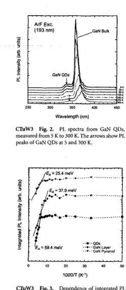
0 10 20 30 40 50
1OOO/T (K-’)
CTuW3 Fig. 3. Dependence of integrated PL intensity on temperature.
The intensity of the GaN QD PL peak is smaller than that of the GaN bulk PL peak, because the volume of GaN QDs is much smaller than that of GaN bulk. The two peaks of 363 and 371 nm are observed from GaN bulk at 300 K. The shorter- wavelength peak is from GaN layer under SiOz, while the longer-wavelength peak is from GaN pyramids, as shown in the previous report6
Figure 3 shows the dependence of integrated PL intensity of GaN QDs, layer under SOz, and pyramids in Fig. 2 on temperature. From Fig. 3, the activation energies are estimated to be 59.4, 37.9, and 25.4 meV in GaN QDs, layer under SO2, and pyramids, respectively. This result indi- cates strong confinement of the carriers exists in GaN QDs.
In summary, for the first time, the fabrication and optical properties of selectively-grown GaN QDs are demonstrated. GaN QDs in AlGaN ma- trix are formed on uniform array of hexagonal GaN pyramids. The PL intensity of GaN QDs is still high at room temperature, which indicates the strong confinement of carriers in GaN QDs. References
1. S . Tanaka, S. Iwai, and Y. Aoyagi, “Self-assem- bling GaN quantum dots on AI,Ga,_xN sur-
2.
3.
4.
5.
6.
faces using a surfactant,” Appl. Phys. Lett. 69, 4096-4098 (1996).
B. Daudin, F. Widmann, G. Feuillet, Y. Sam- son, M. Arlery, and J.L. Rouvikre, “Stranski- Krastanov growth mode during the molecu- lar beam epitaxy of highly strained GaN,” Phys. Rev. B 56, R7069-R7072 (1997). B. Damilano, N. Grandjean, F. Semond, J. Massies, and M. Lerow, “From visible to white light emission by GaN quantum dots on Si (111) substrate,” Appl. Phys. Lett. 75, Y. Nagamune, M. Nishioka, S . Tsukamoto, and Y. Arakawa, “GaAs quantum dots with lateral dimension of 25 nm fabricated by se- lective metalorganic chemical vapor deposi- tion growth,” Appl. Phys. Lett. 64,2495-2497 (1994).
K. Tachibana, T. Someya, S . Ishida, and Y. Arakawa, “Selective growth of InGaN quan- tum dot structures and their microphotolu- minescence at room temperature,” Appl. Phys. Lett. 76,3212-3214 (2000). F. Bertram, J. Christen, M. Schmidt, K. Hira- matsu, S . Kitamura, and N. Sawaki, “Direct imaging of local strain relaxation along the
{ 1101) side facets and the edges of hexagonal GaN pyramids by cathodoluminescence mi- croscopy,”Physica E 2,552-556 (1998). 962-964 (1999).
TUESDAY AFTERNOON
/
CLEO2001
/
241CTUW4 5:30 pm
Observatlon of Glant Ambipolar Diffusion Coefflcient In Thick InGaN/GaN Multiple- Quantum-Wells
Yin-Chieh Huang, Chi-Kuang Sun, Amber Abare,* Stacia Keller,* Steven P. DenBaars,* Graduate Institute of Electro-Optical Engineering, National Taiwan University, Taipei, 10617 TAIWAN, R. 0. C. ; Email: sun@cc. ee. n tu. edu. tw.;
*Department of Electrical and Computer Engineering, University of California, Santa Barbara, CA 93106, USA.
We report our studies on the 2D lateral diffusion behaviors in InGaNlGaN MQWs using optical techniques. Similar to previous observation of the giant ambipolar diffusion coefficient in GaAs-based n-i-p-i superlattices,’ we have ob- served giant ambipolar diffusion coefficient in large well-width InGaN MQWs due to the spatial charge separation by the large built-in piezoelec- tric field. With a well width of 62A, a room-tem- perature ambipolar diffusion coefficient of 2700 f 500 cm2/s was measured.
14 periods Ino., GaN/GaN MQWs we studied were grown on a 2.5 pm thick GaN layer. The barrier widths were held at 43A while the well widths were varied from 17.A to 62A. The bandgaps of MQWs were between 390-430 nm. TRPL studies on these samples revealed a carrier lifetime between 1-4 ns for short well-width samples (12/25A) and a much longer lifetime of >35 ns for the large well-width samples (50/62A), due to the electron/hole wavefunction separation?
The diffusion measurements were performed using standard transmission pump-probe tech- niques with frequency-doubled UV pulses from a
femtosecond Tisapphire laser. With a funda- mental Gaussian mode, the UV pump pulses ex- cited carriers inside the wells with a Gaussian spatial distribution. Due to well confinement, the
photoexcited carriers would diffuse laterally out
of the excitation region but would be still con- fined inside individual wells. Using a delayed probe pulse with the same spot size, its transmis- sion variation would then reflect the carrier den- sity change in the pumping region that was gov- erned by the 2D lateral diffusion. With an equal pump-probe spot size, the initial effective diffu- sion time constant detected by the probe beam can then be related to the diffusion coefficient D and beam radius was:
By measuring the diffusion time constant as a function of beam spot size, the values of D can then be obtained.
Figure 1 shows 390 nm room-temperature re- sponses in the 12A MQW for different beam radii from 4.8 pm to 1 lpm. The measured initial time constant was found to increase from 150 ps up to 700 ps when the spot size was increased from 4.8 pm up to 1 1 p m with a square relation, agreeing with equation (1). The time constant was also found to be independent of the laser ex- citation wavelength and power. Figure 2 plots the measured time constant around time zero vs. pump spot size for the 12A MQW. A value of 400 f 100cmZ/s could be obtained for the 2D lateral diffusion coefficient by fitting.
For thick-well samples, drastic time constant
0 . 0 0 0 -100 200 Tlme Delay (ps) 1
CTuW4 Fig. 1. Transient response of the 12A InGaN/GaN MQW with different spot-sizes. The spot size was increased from 4.8 pm up to 11pm. The laser excitation wavelength was 390 nm.
Beam Radius (pm)
CTuW4 Fig. 2. The measured initial diffu- sion time constant versus pump beam radius for the 12A well-width sample. The dotted line is a fitting according to equation (1) with a value of
242
/
CLEO2001
/
TUESDAY AFTERNOONc
P
0 20 40 M) 00
Well Width (nm)
CTuW4 Fig. 3. Measured 2D diffusion coeffi- cient vs. InGaN MQW well-width.
decrease was observed. 2D lateral diffusion coef- ficient D was found to increase drastically from
400 f 100cm2/s to 2700 k 500cm2/s for well width increased from 12A up to 62A shown in Figure 3. This interesting behavior is similar to the “giant ambipolar diffusion constant” ob- served in GaAs/InGaAs n-i-p-i structures.’ In thick wells, the fast 2D lateral diffusion was due to spatial separation of the charge carriers of op- posite sign which resulted from the strong piezo- electric fields. Due to decomposition of the elec- tron-hole plasma, the attractive Coulomb interaction between electrons and holes was re- duced and did no longer compensate the repul- sion between carriers of the same type as it did in bulk materials.
References
1. K.H. Gulden, et al., “Giant ambipolar diffu- sion constant of n-i-p-i doping superlat- tices,” Phys. Rev. Lett. 66,373-376 (1991). S.F. Chichibu, et al., “Optical properties of InGaN quantum wells,” Mat. Sci. and Eng.
2.
B59,298-306 (1999).
CTuW5 5 4 5 pm
InGaAsN quantum well structures for long- wavelength lasers
Henning Riechert, Infineon Technology, Corporate Research Photonics, D-81730 Muenchen, Germany; Email: [email protected]
We report on the growth of this material by solid source molecular beam epitaxy (MBE) using an RF-coupled plasma source to generate reactive nitrogen from N2. Based on optical and structur- al characterisation we will discuss carrier locali- sation, nonuniformity in composition, local bonding arrangement as well as the influence of the post-growth annealing treatment commonly used for this material.
Material-related performance data of edge- emitting lasers will be given, along with a com- parison of lasers based on InGaAsP and on In- GaAsN. For optimised InGaAsN structures, a decrease of single QW transparency current den- sity down to 100 A/cm2 has been achieved and SQW lasers with threshold current densities as low as 400 A/cm2 for 1000 p m long, as-cleaved resonators have been made. This represents clearly the lowest laser thresholds reported so far for emission around 1.3 pm from the InGaAsN
material system. Based on our results, further po- tential for material optimisation will be dis- cussed.
Finally, we will present results for InGaAsN- based VCSELs on GaAs, emitting more than 0.5 mW near 1.3 pm in cw operation at 25°C.
CTuW6 6:15 pm
The effect of Mg dlffuslon on the contact resistance of low doped pGaN
C.C. Chen, J.L. Yen, and Y.J. Yang, Department of
Electrical Engineering, National Taiwan University, Taipei, Taiwan; Email: yjyang@cc. ee. n tti.edu. tw
In recent years 111-nitride semiconductors have been studied intensively due to its important ap- plications of the short-wavelength optoelectron- ics and electronics. Although the rapid progress on this material system already makes the com- mercial laser diodes (LDs) available,’ still, the critical issue for the device is the lifetime. One of the factors affecting the lifetime is the high p- type contact resistance of the devices, which gen- erates ohmic heating preventing the devices from cw or long-life operation. The obstacles of mak- ing a low resistance p-type contact to GaN are mainly in the difficulty to obtain a high in-situ doping level in p-GaN, and the lack of a metal with a large work function to eliminate or reduce the band offset. For the latter issue, various met- als and annealing conditions were attempted to reduce the p-type contact and some good results have been achieved? However, for the former is- sue, the doping levels in p-GaN are mostly limit- ed to the growth systems and techniques used. Besides few reports, the maximum hole concen- tration in p-GaN is typically -5 x loL7 cm-’, which is about two orders of magnitude lower than that of the conventional 111-V semiconduc- tors such as GaAs for making a good p-type con- tact. The post-growth diffusion, which is a con- ventional way to increase the doping level of as-grown materials, has been unavailable for GaN until recently.’ In this letter we report for the first time that Mg diffusion was applied to low doped GaN (-3 x loL6 cm-’) using Mg3N2 as Mg source to reduce the resistance of contact to p-GaN. The results have consistently showed a reduction of contact resistance by -1.5 orders of magnitude.
A MOCVD grown p-GaN wafer with a hole concentration of 3 x 10l6 cm-’ and a thickness of -2 pm was used for this study. To conduct the Mg diffusion into p-GaN, the sample was sealed with Ma3N2 powder in a vacuumed quartz am- poule and put into a 950°C for 5 min for anneal- ing. Secondary ion mass spectroscopy (SIMS) was used to determine the Mg diffusion profile. Hall measurement was used to characterize the hole concentrations of the sample before and af- ter diffusion. To understand the effect of surface treatment on the contact to p-GaN, the samples were also processed with and without 20 min Aqua regia etching for comparison. A Ni/Au film was deposited on the sample and annealed at 600°C for 1 min to form an ohmic contact. The contact resistance was measured by a transmis- sion line model (TLM) using a linear configura- tion of 200 x 80 pm2 metal pads with spacing varied from 4 to 40 pm linearly in 10 steps.
The measured hole concentration of the p-
GaN sample increased from 3 X loL6 cm-’ to 3 X cm-’ after Mg diffusion. Since the diffusion region with the Mg concentration >5 x l O I 9 cm-’ observed from SIMS was only -0.2 pm thick, based on a -2 pm thick p-GaN layer, the actual hole concentration near the surface of GaN can be estimated to be >3 x 10” cm-’, which was one order higher than the typical maximum hole concentration obtained from the in-situ doping in crystal growth. Fig. 1 shows the current-volt- age (I-V) curves of the Ni/Au contacts to p-GaN wafers under four different process conditions: the as-grown as well as the diffused samples each with and without surface treatment (Aqua regia etching). It clearly indicates that the resistance of the diffused samples was much lower than that of the as-grown samples. There is a turn-on of -1 V on the I-V curve of the diffused samples without surface etching, indicating the existence of oxide on the GaN surface? With the Aqua regia etching to remove the oxide a linear I-V curve showing an ohmic contact was obtained.
Fig. 2 shows the results of the TLM measure- ment on the four different wafers same as those used in Fig. 1. The contact resistance was deter- mined to be 2.73 R-cm2 for the as-grown wafer, 6.86 x R-cm2 for the as-grown wafer with surface treatment, and 1.93 x lo-’ R-cm’ for the diffused wafer with surface treatment respective- ly. These results indicate that the contact resis- tance was reduced by -1.5 orders of magnitude by the surface etching only: and improved by an- other -1.5 orders of magnitude by the Mg diffu- sion. The improvement from the Mg diffusion can be explained as the following model Since the transport property of the metal-semiconduc- tor contact is dominated by the tunneling mech-
0 no&maaMlt
.
w i l h & ” m t4 . 2 0 2 4
Voltage (V)
CTuW6 Fig. 1. Current-voltage curves of the samples processed under four different condi- tions.
Distance (rm)
CTuW6 Fig. 2. Contact resistance measured
by the transmission line model on the four dif- ferent samples as same as those used in Fig. 1.