Improved asymmetrical half-bridge converter using
a
tapped output inductor filter
Y.-H. Leu and C.-L. ChenAbstract: The asymmetrical half-bridge converter (AHBC) has the attractive features of zero
voltage switching (ZVS) and voltage clamping. However, the converter is not suitable for wide input voltage range applications since it has the problem of a 50% maximum allowable duty cycle. A new AHBC topology with a tapped output inductor filter is proposed that not only extends the allowable operating duty cycle but also makes the ZVS condition less stringent. The principle of operation is explained and analysed. Experimental results obtained from a 24V/3 A prototype are presented, which illustrate converter function and verify the analytical results.
List of symbols
D
ZSl-pk zS2-pk imDC i&k lmpk ZP i D I iD2 ZDI -RMS ID2-RMS V C T transformer A e L M L M LI leakage inductor LI leakage inductance n NP NI N2duty cycle of switch SI peak current of switch S I peak current of switch S2
average value of magnetising current positive peak value of magnetising cur- rent
negative peak value of magnetising cur- rent
instantaneous current of leakage inductor LI
instantaneous current of output rectifier
D1
instantaneous current of output rectifier
D2
root-mean-square current of output recti- fier DI
root-mean-square current of output recti- fier D2
average voltage across blocking capacitor .-
Cb
effective cross-sectional area of the core of
transformer T
magnetising inductor of transformer T
magnetising inductance for transformer T
turns ratio of transformer T
number of turns of transformer primary winding
number of turns of the first winding of the tapped-inductor
number of turns of the second winding of the tapped-inductor
0 IEE, 2003
IEE Proceedings online no. 20030377 doi: 10.1049/ip-epa:20030377
Publication date: 12th May 2003. Paper first received 10th July 2002 and in revised form 6th February 2003
The authors are with the Graduate Institute of Electronics Engineering & Department of Electrical Engineering, National Taiwan University, Taipei, Taiwan
k
L N 1
L N 2
%I2 current flows through LN2
TS switchng period of converter
fs
switching frequency of converterwindings ratio coefficient, whch is de- fined as N1/N2
inductance of the first winding of the tapped-inductor
inductance of the second winding of the tapped-inductor
1 Introduction
For low to medium power level applications, topologies derived from an asymmetrical half-bridge converter (AHBC) have been widely discussed due to their smaller component counts, lower stress on the power switch, and soft-switching phenomenon [ 1-81. Among these topologies, the AHBC has a higher efficiency due to its lower root- mean-square (RMS) current of the output rectifiers. Fig. 1 shows the basic circuit of the converter. However, the converter has the problem of a 50% maximum allowable duty cycle [ 3 4 ] . This makes the converter unsuitable for operating within a wide input voltage range. Moreover, the voltage stress of the output rectifier depends on the operating duty cycle. If the operating duty cycle is adjusted
to 50%, these two rectifiers will be under the same voltage
stress. Thus, a lower voltage drop diode can be used and the conductive and switchng loss
of
the rectifiers can be reduced.In recent years, little effort has been expanded on
extending the maximum allowable duty cycle of an AHBC
%S
Fig. 1 SimpliJ5ed schematic of the AHBC
[7, 81. The two-transformer AHBC was proposed in 1999 [7]. By tuning the individual turns ratios of the two transformers, the maximum allowable duty cycle can be extended to be over 50%. However, this is at the price of an increased complexity and cost.
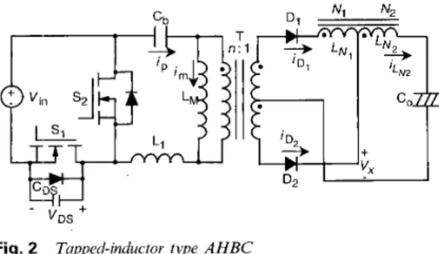
The problem of duty cycle limitation in an AHBC will now be addressed. A modified circuit will be proposed. Fig. 2 shows the basic circuit diagram. As the Figure indicates, the converter has the same components count as in Fig. 1. The only difference is that in the output inductor filter, a tapped-inductor replaces the one-winding inductor. By tuning the ratio of the number of windings of the tapped-inductor, the operating duty cycle of the converter can be extended to be over 50%. Compared with a conventional AHBC, the zero voltage switching (ZVS) condition and current stress on the power switch of the proposed converter are reduced. Additionally, the basic principle of operation and its steady-state characteristics will be analysed. The design considerations are given according to the analysis. To demonstrate the effectiveness of the characteristic performances, experiments are carried out with a 24V/3 A, 120 kHz prototype.
y w +
vDS
Fig. 2 Tupped-inductor type AHBC
2 Circuit description of the proposed converter
Referring to Fig. 2, the power switches S I and S2 are driven alternately, but with a short blocking interval. LI represents the leakage inductor of the transformer T, whde CDs
represents the junction capacitor of SI and S2. N I , N2 are the two windings of tapped-inductor, with the windings ratio coefficient, k, being is defined as NI/N2. Note that, when k is zero, the AHBC can be considered as being a special case of the proposed converter. The principle of operation and the steady-state analysis are illustrated with the following assumptions:
1. the converter operates under steady-state conditions; 2. the output filter operates in continuous conduction mode; 3. switching components are ideal; and
4. Cb is large enough, so that the voltage across it is constant.
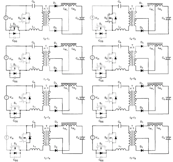
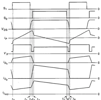
The operating principle for one switching cycle is divided into eight stages, and the equivalent circuits for each one is illustrated in Fig. 3. The solid lines denote the current conducting paths. Fig. 4 shows the key waveforms of the converter. The operating behaviour of the converter will now be described.
to-tl: SI and DI conduct before to. Cb, LM, and LI are charged by the input source. The transformer provides the electrical isolation between the input and the output sides, and transfers energy to the output. During this
interval, the tapped-inductor works as a one-winding inductor and stores energy.
t I-t2: SI is turned off at t I . CDs is charged by the primary current, which is the combination of the magnetising current and the reflected output current. Because the transient interval is so short, the actual resonant charging manner is approximated as a linear charging characteristic. t2-t3: At t2, D2 is forward biased. The output current circulates through D l and D2. LI and CDs form a resonant network. During the interval, the voltage V D S ( t ) and the primary current ip(t) can be formulated as:
i p ( t ) = i p ( t 2 ) cos w r ( t - t 2 ) (1)
where, or = 1/J-, k = N I / N 2 .
t3-t4: After CDs is charged to the input voltage at t 3 , the
anti-parallel diode of S2 starts to conduct. To achieve ZVS operation and reduce the conduction loss for S2, the switch should be turned on before the primary current changes direction. The voltage across the leakage inductor can be expressed by:
[I + k ( l -D - D )
1
VL, = K n ( 3 )
The negative voltage across the leakage inductor makes the primary current ip, decrease in a linear manner. This causes the current of Dl to quickly decrease. When the current has reduced to zero, the device is off and this stage ends.
t4-t5: During this interval, the energy stored in the tapped-inductor starts to discharge. Because the inductor remains at a smaller value, the reflected current is larger than that in the AHBC. The larger reflected current contributes to the ZVS operation of the low-side switch, SI.
tytfj: At t5, S2 is turned off. The primary current
discharges CDs, and VDS decrease linearly. This stage ends when the VDs increases to forward bias Dl.
t6-t7: In t h s stage, D1 and D2 again simultaneously
conduct. LI and CDs resonate. The VDs(t) and ip(t) are found as:
i p ( t ) = i p ( t f j ) cos W , ( t - tfj) (4)
I _
Supposing the energy stored in LI is sufficient to discharge CDs completely, the voltage across CDs will be zero. The primary current can flow through the anti-parallel diode of
s,.
tTt8: After VDs decreases to zero, the voltage across the leakage inductor is:
The positive voltage causes a rapid change rate in the primary current and D2 current. Before the primary current changes polarity, SI should be turned on to ensure ZVS operation. At tg, the current of D2 is zero. D2 turns off, and another switching cycle starts ( t g = to).
IEE Proc.-Electr. Power Appl., Vol 150, No. 4, July 2003 418
i i . . e.... .
p
i
;
. . . . ... i ; ... t , - t . .... : . . . i si . f"" ... ... )cl ... ' U . I T!..
; q j D, i ...*
... i cDS ... s : : i.f ; Vi, 21 *.; ii s ,
' i ..i.. "$" "]" 0 ... )II. .... * ... ... .... : ... . . ... T' ... ..* ... : ... i > ... : cDS * 3 4 4Fig. 3 Eight topological states of the proposed converter
3
This section analyses the key improved characteristics of using a tapped-inductor in a AHBC.
Characteristics of the proposed converter
3.1 Static voltage transfer ratio
In a switching cycle, the average flux variation of the magnetising inductor should be zero. Therefore, the voltage transfer ratio can be derived as:
(7)
Also, the maximum allowable operating duty cycle of the converter is:
(8)
( k + I ) -
d
m
k
Dm,, =
From (7), the voltage transfer ratio is a function of k and
D.
The influence of different k andD
values on the voltage transfer ratio is shown in Fig. 5. It is found that theIEE Proc-Electr. Power Appl.. Vol. 150, No. 4, July 2003
... ..-.. : ;,.:... + ': Vin
4
.... i ; s, . ...:
$"";'
: ... . . . . : .... t ... "?""""' ... )cl ... * . . . . ... > ... : . . : : ... i i ... cDSmaximum allowable duty cycle of the converter can be extended to be over 50%. In steady-state operation, the voltage stress of the rectifiers is:
VO VD, = - 1 - D VO VD2 = - D (9)
From (9) and (lo), if the operating duty cycle is adjusted to 50%, the rectifiers will be under the same stress.
3.2
RMS
current of the output rectifierIn order to simplify the analysis, the dead time between the conduction intervals of the power switches is neglected. Only the stages to-t, and t4-t5 are discussed in t h s section. The simplified operational circuits for these two stages are shown in Figs. 6a and 6b. During the D interval, the two inductors are in series and are charged by the input source. During the (1-D) interval, the energy
Fig. 4 Theoretical waveforms on some key components c 2-
.
0 b a b C Fig. 6a Simplified topological state: S I on,
b Simplified topological state: S2 on,
c Simplified current waveforms of L N ~
Fig. of k
D
5 Voltage transfer ratio as a function of 0, for dflerent value
The RMS current of the two rectifiers are:
stored in the two inductors is transferred to the output by L N ~ . The simplified current waveform of the L N ~ is shown in Fig. 6c.
As the diagram indicates, the relationship of the I,, Ib, I,, I d , and Io can be formulated as the following equations:
(NI
+
N2)Ib = N2jcN2Id = (N1
+
N2)Ia(11)
(12)
(I,
+
Ib)D -k (IC + I d ) ( 1 - 0)(13) Io =
\ 2
I b =Ia
+
mlDT, (14) whereBy solving (1 1H15), the currents
Z
,
and I, can be expressedas: (1 - 2 0 ) vo -Ts (16) 10
z -
a - 0+
(1+
k)(l
- 0) - 2(k+
l)(k
+
2)LN2 whereFig. 7 shows the RMS current ratio of the two rectifiers (IDRatio = I D ~ ~ ~ / Z D ~ ~ ~ ) with different winding ratios (k = 0 and
k
= 1). It is found that no matter what the ratio is, the larger portion of the output current flows through D2. At this point, the importance of extending the operating duty cycle is again highlighted. If the operating duty cycle is augmented, a lower voltage drop diode can be used. Moreover, increasing the windings ratio, the uneven current distribution of two rectifiers is worse.2.5 - 2.0 - 1.5 - A h A ; 1 . . 1 . 1 ~
;::I
, , , , , , , , , , 0 0.50 0.75 1.00 1.25 1.50 1.75 2.00 2.25 2.50 2.75 3.00 I,, A Fig. 7the output current, ,for dvjirent values of k
RMS current ratio of two output rectiJiers as a function of
3.3 Maximum operating flux density of the transformer
Since the converter is controlled with an asymmetrical duty cycle, the average magnetising current is not zero, but a DC value. The DC value of the magnetising current lowers the transformer utilisation rate. In order to avoid saturation, the average magnetising current has to be taken into consideration in the design. The average input current (I,,,) and the output current (Io) should obey the following relationship:
(21)
I
---[
I,,, - 1 ( k+
2 P ( 1 - D )lo II l + k ( l - 0 )
The relationship between the average input current and the average magnetising current (I,,Dc) is expressed by:
Substituting (21) into (22) yields: 10 (1 - 2 0 )
4I"
= -t~ 1 + k ( l - D )
The average magnetising current is a function of the duty cycle and the winding ratio of the tapped-inductor. The relationship between the average magnetising current and the operating duty cycle for different winding ratios is shown in Fig. 8. It is found that the optimal operating duty cycle of the converter is 50%. If the converter operates at this point, the average magnetising current will be zero. Moreover, a larger winding ratio for the tapped-inductor results in a smaller DC value of the magnetising current. Taking the AC swing into account, the peak magnetising
-0.8
:",:",
-1 .o 0
:
0.1 0.2 0.3 0.4 0.5 0.6 0.7 0.8 0.9 1.0D
Normalised DC value of the magnetising current as a Fig. 8
function of 0, j o r dferent vulues of k.
current of the transformer is:
.- 10 ( 1 - 2 0 ) nVo[l + k ( l - 0 ) ] Ts
~ (25)
zlllPk =
;
1 + k( 1 - 0 ) - ( k + 2 ) 2LMThe maximum operating flux density of the transformer is: [IINPA,;~
+
k ( 1 - D ) ] + 2NpA,(k+
2 )B,llax =
x lo8 (26)
LMrO(1 - 2 0 ) nVo[l + k ( l - 0 ) T s ]
3.4
ZVS
transitionThe ZVS condition for the two switches can be derived from (2) and (5). Before S2 is turned on, V D S should
increase to match the input voltage. Before S I is turned on, VDs should decrease to zero. Equations (27) and (28) quantitate the ZVS condition for S2 and S I , respectively.
where the current ip(t2) and ip(t6) can be approximated as:
From (27) and (28), it is found that whether or not ZVS operation is achieved depends on how much energy is stored in L,. A larger leakage inductance is helpful to achieve ZVS operation of both switches. Fig. 9 shows the required value of the leakage inductance for ZVS operation at different winding ratios for the studied converter. As the Figure indicates, the ZVS condition of SI is stricter than S2. Utilising a tapped-inductor in the output filter, means that the ZVS condition for S2 can be reduced.
4 Design considerations
In this Section, the design considerations of the proposed converter are developed according to the analytical results. They can be described as follows:
4.
I
Operating
duty cycleDetermining the operating duty cycle is the first step. The optimal operating duty cycle of the AHBC is 50%. If the converter operates at t h s point, not only will the output rectifiers be under the same stress, but also the average magnetising current will also be zero. Equation (8) formulates the maximum allowable duty cycle of the proposed converter. If the winding ratio of the tapped- inductor is one, then the maximum allowable duty cycle can be extended to 0.586. In order to bear the load disturbance and duty loss, it is recommended to set the operating duty cycle it to be 40%.
The drawback of using a tapped-inductor is that an unbalanced output current flows through the output rectifiers. As indicated in Fig. 7, the larger k is, the more parts of the output current flow through DZ. Therefore, it is necessary to reconcile the winding ratio of the tapped- inductor with the operating duty cycle.
" 4 3
f-\
2 0'i
.
I I I I I , , , I 0 0.25 0.50 0.75 1.00 1.25 1.50 1.75 2.00 2.25 2.50 2.75 3.00 10, A 1.2 Q 1.1 - - Y .-z
1.0 - 0 . 7 ' " " ' " ' ' " ' 0 0.25 0.50 0.75 1.00 1.25 1.50 1.75 2.00 2.25 2.50 2.75 3.00 a + k = O -+- k = lr'\
0 0.25 0.50 0.75 1.00 1.25 1.50 1.75 2.00 2.25 2.50 2.75 3.00 Io, A b Fig. 9ZVS range operation of the switches, j o r dijfkrent values of k a Required values for S2
b Required values for SI
The required leakage inductance as a function of dgferent
4.2 Power switch
Referring to Fig. 4, the peak currents of S I and S2 ( i s l - p k ,
i ~ 2 - ~ k ) are the same as the positive and negative peak values of the primary current, respectively. These currents can be expressed as: i S 1 -pk = i p ( t 2 ) f0 + k ) ( l - D ) 2 ( k
+
l ) ( k+
2) LN2 (1 - 2 0 ) Vo+
1 Kn(l - D ) 2 LM+
I m D c+
- (31) (32)Figs. IOU and 10b show the peak currents of S I and
S2 (is1 + k , is2-pk) under different loadings for different
422 0.6' ' ' " ' " ' ' " ' 0 0.25 0.50 0.75 1.00 1.25 1.50 1.75 2.00 2.25 2.50 2.75 3.00 l o , A b Fig. 10
current, f o r dgerent vulues of k
a Peak current values of SI
b Peak current values of S2
Current stress of the switches us a junction o f t h e output
values of the windings turn ratio (k). When k = 0, the peak current stress of SI is 1.4A at full load, and the stress of S2 is 0.85 A. When k = 1, the peak current stress of both switches is about 1.1 A at full load. This shows the current stress of the switches is more balanced by using a tapped-inductor in the AHBC. Additionally, the voltage stresses of the switches is the input voltage.
4.3 Transformer magnetising inductors
The D C magnetising current of the transformer affects the utility rate of the magnetic material. In a practical design, the DC value has to take this into account. If the useable flux density of the material is BSat, the maximum allowable magnetising inductance can be derived from (26), and the value is:
I\
IO( 1 - 2 0 )
4.4 Leakage inductor
As the above-mentioned, in order to acheve a ZVS operation of the switch, the leakage inductor must store sufficient energy to charge/discharge CDs. If the ZVS operating range is chosen, the minimum value of the required leakage inductance can be derived from (28).
5 Experimental results
A 120 kHz 24V/3 A prototype is implemented for verifica- tion. The specifications of the converters are:
input voltage: 400 V DC; output voltage: 24 V DC; maximum load current: 3 A; switching frequency: 120 kHz; normal operation duty cycle: 0.34. The circuit parameters are listed as:
power switches S I and S2: Fuji, 2SK2645, RDs(on) = 1 R;
output diodes D I and DZ: IR, lOCTQ150, V,=0.73V; transformer T: A , of core: 1 cm2; WI: 27 turns of Litz wire 50 x 0.1 mm; W2: 4 turns of Litz wire 50 x 0.1 mm;
tapped-inductor: k = 1, LN1 = 15 pH, LN2 = 15 pH; magnetising inductance L M : 470 pH;
leakage inductance LI: 20 pH.
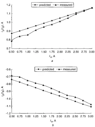
Fig. 11 shows the experimental waveforms on some key components of the studied converter under half-load operation. These waveforms are arranged in the same order as in Fig. 4. It is shown that the experimental results coincide with the analysis. As mentioned earlier, the current ip(t2) and iP(@ play crucial roles in the ZVS operation of the switches. Fig. 12 shows the predicted and experimental values of these currents. It is shown that the calculated values are very close to the measured values. Fig. 13 shows the predicted and experimental RMS currents of D I and D2 under different loadings. The calculated current of D1 is larger than the experimental ones, but the result is the opposite in DZ. The reason for this is that the duty loss of the converter is neglected in the analysis. In order to
Fig. 11
is I usldiv)
Experimental wavejorms on key components. (Time scale
0.50 0.75 1.00 1.25 1.50 1.75 2.00 2.25 2.50 2.75 3.00 I,, A a t.predicted t- measured -OX
r
-1.21 ' ' ' ' ' ' ' ' ' ' 0.50 0.75 1.00 1.25 1.50 1.75 2.00 2.25 2.50 2.75 3.00 I,, A b Fig. 12as a function of the output current
a The values at time, t 2
b The values at time, t6
Experimental undpredicted values o f t h e primary current
1.4 - --t predicted -k- measured 1.2. 1.0. 4 0.8 - 01 " " ' ' " " 0.50 0.75 1.00 1.25 1.50 1.75 2.00 2.25 2.50 2.75 3.00 10, A a 3.25 - 3.00 - 2.75 - 2.50 - 2.25 -
-
predicted t- measured 0.50 0.75 1.00 1.25 1.50 1.75 2.00 2.25 2.50 2.75 3.00 I,, A b Fig. 13as a junction of' the output current a the value of D,
b the value of D2
Experimental undpredicted RMS current of the rectgers
regulate the variation of the output voltage caused by the load disturbance, the operating duty cycle of S I must be increased, t h s will result in more current through D1 and less through D2. The overall efficiency was measured under different values for the output current range at different winding ratios, as shown in Fig. 14. The efficiency of the tapped-inductor type AHBC is hgher than that of non- tapped-inductor type under a heavy load. However, the efficiency is worse under a light load. Ths is because using a tapped-inductor in a AHBC is not conducive to the ZVS
operation of S I under light load. The efficiency of the two converters exceeds 90% under full load operation.
701
//
6 5 L J S s " " * * " '
0 0.25 0.50 0.75 1.00 1.25 1.50 1.75 2.00 2.25 2.50 2.75 3.00
10, A Fig. 14
current, for dflerent values of k
The niecisured efjciency as U function of the output
6 Conclusions
The AHBC is considered a suitable topology for low to medium power level applications. However, it has the problem of a 50% maximum allowable duty cycle. A
new AHBC topology using a tapped output inductor filter has been proposed to solve the problem. From the analytical and experimental results, several advantages of a larger windings ratio coefficient of the tapped- inductor have been observed: (i) the maximum allowable duty cycle of the AHBC can be extended; (ii) the
ZVS condition and current stress on the power switches can be reduced; (iii) the transformer utilisation rate is better; and (iv) a higher efficiency is obtained under a heavy load.
The only shortcoming is that the uneven current distribution of two rectifiers would be worse.
References
Heme, C. P., Lo, D. S., Martin, J., and Hubert, C.: 'Zero-voltage resonant transition switching power converter', U.S. Patent 5057986, Oct. 1991
Seo, D. H., Lee, 0. J., Jim, S. H., and Park, J. S.: 'Asymmetrical PWM
flyback converter'. Proc. Power electronics specialists Conf. (PESC), 2000, pp. 848-852
Ninomiya, T., Matsumoto, N., Nakdhdra, M., and Harada, K.: 'Static and dynamic analysis of zero-voltage-switched half-bridge converter with PWM control'. Proc. Power electronics specialists Conf. (PESC), 1991, pp. 23&237
Imbertson, P., and Mohan, N.: 'Asymmetrical duty
cycle permits zero switching loss in PWM circuits with no
conduction loss penalty', IEEE Trans. Ind A p y l , 1993, 29, (I), pp. 121-125
Korotkov, S., Meleshin, V., Miftakhutdinov, R., and Fraidlin, S.: 'Soft- switched asymmetrical half-bridge DC/DC converter: steady-state analysis: an analysis of switching processes'. Proc. IEEE Int. Tekcommunicdtions Energy Special Conf. (TELESCON), 1997, pp.
177-184
Oruganti, R., Heng, P.C., Guan, T.K., and Choy, L.A.: 'Soft-Switched DC/DC Converter with PWM Control', IEEE Trans. Power Electron, Miftakhutdinov, R., Nenichinov, A., Meleshin, V., and Fraidlin, S.: 'Modified Asymmetrical ZVS Half-Bridge DC-DC Converter'. Proc. Applied power electronics Conference and Exposition, 1999, pp. 567- 574
Chen, W., Xu, P., and Lee, F. C.: 'The Optimization of Asymmetrical Half Bridge Converter'. Proc. Applied power electronics Conference and Exposition, 2001, pp. 703-707
1998, 13, (I), pp. 102-1 14