子計畫五:本地振盪電路之研製(3/3)
計畫類別: 整合型計畫 計畫編號: NSC92-2219-E-002-005- 執行期間: 92 年 08 月 01 日至 93 年 07 月 31 日 執行單位: 國立臺灣大學電信工程學研究所 計畫主持人: 瞿大雄 報告類型: 完整報告 報告附件: 出席國際會議研究心得報告及發表論文 處理方式: 本計畫可公開查詢中 華 民 國 93 年 11 月 2 日
38-GHz 無線收發系統關鍵元組件技術
-
子計畫五:本地振盪電路之研製(1/3)(2/3)(3/3)
計畫類別:□ 個別型計畫 ■ 整合型計畫
計畫編號:NSC 90-2219-E-002-106-
NSC 92-2219-E-002-018-
NSC 92-2219-E-002-005-
執行期間:
90 年 8 月 1 日至 93 年 7 月 31 日
計畫主持人:瞿大雄
共同主持人:
計畫參與人員:
成果報告類型(依經費核定清單規定繳交):□精簡報告 ■完整報告
本成果報告包括以下應繳交之附件:
□赴國外出差或研習心得報告一份
□赴大陸地區出差或研習心得報告一份
■出席國際學術會議心得報告及發表之論文各一份
□國際合作研究計畫國外研究報告書一份
處理方式:除產學合作研究計畫、提升產業技術及人才培育研究計畫、列管 計畫及下列情形者外,得立即公開查詢 □涉及專利或其他智慧財產權,□一年□二年後可公開查詢執行單位:
國立台灣大學電信工程學研究所
中 華 民 國
93 年 10 月 日
本計畫為一三年計畫(90年至93年),配合整合型計畫「38-GHz無線收發系統關鍵元組 件技術」,進行其關鍵元組件-本地振盪器之研發。本計畫之重點有三:一為研製一適用於 38-GHz無線收發系統之本地振盪器。二為建立振盪器陣列之理論推導、分析公式、電路研 製及實驗量測。三為進行振盪器陣列之應用研究。 本報告係敘述三年之研究成果,以耦合振盪器陣列的相位控制為基礎,研究發展 三項新的應用,包括 N 推式諧波振盪器、反向輻射天線陣列及方向掃瞄與極化調 整天線陣列等。有關適用於38-GHz 無線收發系統之本地振盪器研製,已配合總計畫完 成,並於分年報告中敘述,本報告則專注於敘述振盪器陣列之三年研究成果。 首先,第三章將推-推式振盪器的理論推廣至三推式、四推式、乃至於 N 推式 諧波振盪器。不同於以往傳統採用線性模態分析方法,本章提出之分析係以耦合 振盪器理論為基礎,藉由調整不同的相位關係與適當的導通時間,將其產生的 N 階諧波成分,因同相而加成,而其他的低階諧波與基頻成分,則會因相位的對稱 性而相互抵銷。由於功率合成係使用被動電路,因此較不易受限於串接形式中, 輸出級元件的功率輸出能力。本章除敘述理論推導,並分別對二推式、三推式及 四推式的諧波振盪器提出實驗驗證。 第四章介紹一種新的相位共軛電路,並將其應用在反向輻射天線陣列。相位 共軛電路係利用次諧波注入鎖定自振盪混波器所構成的平衡式電路架構,將次諧 波的輸入信號轉換為其相位共軛信號。相較於以往的外差式陣列,此電路不需提 供外加的兩倍頻本地振盪信號。由於振盪器的注入鎖定現象,輸出信號會被鎖定 至輸入信號相同的頻率;也由於注入鎖定現象,使其得到一定的操作頻寬。本章
證。 最後,第五章則敘述使用二維的耦合振盪器陣列,研製方向掃瞄與極化調整 天線陣列。利用二維平面上的相位分佈,其中一個維度的相位變化做方向掃瞄, 另一維度的相位變化對應到極化的改變,則可同時達成方向掃瞄與極化調整的功 能。採用振盪信號的二次諧波,將陣列元素間的可用相位差倍增至 ,使系統 得到穩定的操作模態。本章分別對水平極化、垂直極化、左旋圓極化與右旋圓極 化波的方向掃瞄能力,提出理論分析與實驗驗證。 o 180
This is a three-year project to conduct research and development of microwave oscillator technologies. There are three major tasks involved. One is to develop the local oscillator for the 36GHz transceiver. Two is to develop the basic theory and experiments of oscillator array. Three is to develop the novel applications of oscillator array.
On the basis of the phase control ability of mutually coupled oscillator arrays, this report investigates the novel applications for the high-frequency signal source and active antenna array systems. Both the theoretical analysis and the experimental implement are emphasized. The three new applications presented are an N-th harmonic oscillator, a retro-directive antenna array, and a beam-scanning and polarization-agile antenna array. As for the local oscillator for the 36GHz transceiver, it was given in the concise reports.
Firstly, in Chapter 3, the design concept of push-push oscillators is extended to triple-push, quadruple-push and hence N-push harmonic oscillators. Conventionally, this kind of problems is dealt with by linear mode analysis. The design principle in this dissertation is based on the injection-locking theory. The desired harmonic component can be selected by tuning the relative phases of the coupled oscillators and the conduction angles of voltage-clamping circuits. As the output phase-shifted signals of the coupled oscillators are properly shaped and combined, the desired harmonic components are constructively generated and lower-order harmonic components are suppressed. This structure can be
combined in a passive circuit, it does not suffer from the power limit of the output device in the cascade structure. The circuit structure is presented and verified experimentally in second-harmonic, third-harmonic and fourth-harmonic oscillators.
In Chapter 4, a novel phase conjugation circuit and its application to retro-directive antennas are presented. The phase conjugation circuit uses a balanced circuit structure with subharmonically injection-locked self-oscillating mixers (SILSOMs) oscillating at ω. An input signal at ω/2 is converted to its conjugated signal with no external source required for LO signal pumping, and the output signal frequency is locked at the same frequency of the input signal. The developed phase conjugation circuit is implemented with active antennas to become a retro-directive antenna array. Both the theoretical and measured results of phase conjugation and retro-directive performance are presented.
Finally, a two-dimensional mutually coupled oscillator array is studied in Chapter 5 for the application of a beam-scanning and polarization-agile antenna array. In the antenna array design, the polarization agility is considered as one of the two dimensions (or y-direction) with the other dimension (or x-direction) for beam scanning of a two-dimensional oscillator array in x-y plane. The array radiation direction can be scanned for the selected polarization states including linearly polarized, left-hand and right-hand circularly polarized states. Well-defined phase differences among oscillators for beam scanning and polarization agility are given by utilizing the second-harmonic signal. The
antenna array are verified experimentally and shown to have the potential for adaptive antenna array applications.
摘要
................................ iiA
BSTRACT ............................ ivC
ONTENTS ............................ viC
HAPTER1
I
NTRODUCTION ................. 1 1.1 Research Motivation ................... 1 1.2 Literature Survey .................... 2 1.3 Contributions ...................... 6 1.4 Chapter Outlines ..................... 7C
HAPTER2
B
ASICP
RINCIPLES ............... 152.1 Injection-locked Oscillator ................ 16 2.1.1 Equivalent Circuit Model ............. 16 2.1.2 Time Domain Dynamic Analysis .......... 17 2.1.3 Subharmonic and Harmonic Injection ........ 20 2.2 Coupled Oscillator Array ................ 21 2.2.1 Nearest-neighbor Coupling Condition ......... 22 2.2.2 Phased Array Using Oscillator Array ......... 23 2.3 Harmonic Oscillator .................. 24 2.3.1 Circuit Topologies ................ 24 2.3.2 Push-push Oscillator ............... 25
C
HAPTER3
N
-P
USHH
ARMONICO
SCILLATOR ........ 333.1.2 Design Philosophy ................ 34 3.1.3 Nonlinear Frequency Conversion .......... 35 3.1.4 Power Combining ................ 36 3.1.5 Phase Control .................. 37 3.1.6 Phase Noise .................. 38 3.2 Circuit Implementation.................. 38 3.3 Results ........................ 39 3.4 Summary ....................... 40
C
HAPTER 4R
ETRO-DIRECTIVEA
NTENNAA
RRAY......514.1 Introduction ...................... 52 4.2 Design and Formulations ................. 54 4.2.1 Design Principles ................. 54 4.2.2 Practical Consideration .............. 57 4.4 Circuit Implementation.................. 61 4.4.1 Phase Conjugation Circuit ............. 62 4.4.2 Retro-directive Antenna Array ........... 63 4.5 Results ........................ 63 4.5.1 Phase Conjugation Circuit ............. 63 4.5.2 Retro-directive Antenna .............. 65
4.6 Summary ...................... 67
5.1 Introduction ..................... 84 5.2 Design and Formulations ................. 86 5.3 Results ........................ 92 5.4 Summary ....................... 94
C
HAPTER6
C
ONCLUSIONS ................. 109 6.1 Summary ...................... 110 6.2 Future Work ..................... 111R
EFERENCES .......................... 113A
TTACHMENT 1出席國際學術會議心得報告
.......... 120A
TTACHMENT 2出席國際學術會議發表之論文
.......... 122 . . . . . . . . . . . . . . . . . . . .I
NTRODUCTION
1.1
Research Motivation
With the rapid development in the personal wireless communications, the requirements of compact circuit size, low cost, high efficiency, and high integrity for RF circuits draw more and more attention. With the aid of the maturity of semiconductor techniques, active antenna techniques [1], which integrate the passive antennas and the active circuits, become possible. Especially at high frequency, the decreased antenna size makes this concept even more practical.
One of them is the versatile capability of phase control. A lot of researches are devoted to this topic, and find various methods to analyze and control the phase distribution in one-dimensional or two-dimensional arrays [2]-[11]. Moreover, the oscillator can provide high output power itself. That means one can control the phase distribution of the signal sources in one-dimensional or two-dimensional surfaces. It shows the potential of applications on active antennas. There are still a lot of interesting applications of mutually coupled oscillator array to be discovered. This report is devoted to developing three new applications, especially about active antenna array, based on the theories derived earlier.
1.2
Literature Survey
As an oscillator is injected by an external signal with frequency close enough to its free-running frequency, the oscillating output signal follows this external signal in frequency, and is insensitive in amplitude. While the injection frequency moves away, the oscillator returns to the free-running mode. This phenomenon is called injection locking [12]-[15]. The phase noise of injection-locked oscillators is determined by the small external reference signal provided this reference signal is stable enough. This property is widely used to produce a stable and high power source at microwave and millimeter-wave frequency.
Injection-locking phenomenon was first reported theoretically by Van der Pol [12] in 1927. Then Adler [13] developed the theory of this phenomenon for
electric oscillator in 1946. In 1973, Kurokawa [14] applied this theory to microwave solid-state oscillators using negative resistance oscillator model. It describes the property of injection-locked oscillator by mathematical formulas and experiments. That established the fundamentals for the researches of injection-locked oscillators in microwave and millimeter-wave nowadays.
In applications such as radar, communication links, and astronomy, many systems require high output powers and antennas with very directive radiation patterns to deliver the desired signal efficiently [16]-[19]. To produce these pencil beams, large-reflector antennas [20] have been used extensively. As these beams are often required to point to various directions, mechanical beam scanning thus was developed. This system tends to be large, bulky, and slow.
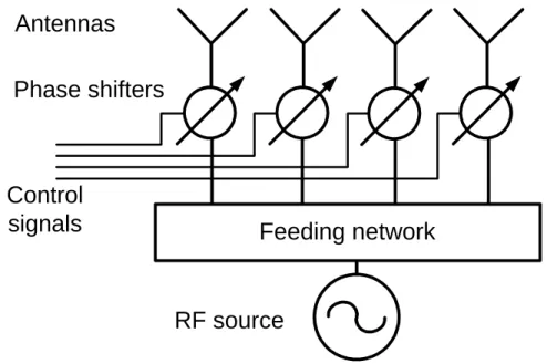
Besides reflector antennas, large antenna arrays consist of multiple smaller antenna elements can also provide narrow, high-gain pencil beams. For beam scanning, antenna arrays may utilize electric method rather than mechanical one. This kind of antenna array is generally called phased array [19]. That dramatically improves the beam-scanning speed. In addition, planner antenna arrays are not as bulky as comparable reflector antennas. Figure 1.1 illustrates the operation of the beam scanning phased array.
However, phased array uses phase shifters in each antenna element to achieve the desired aperture phase distribution [19]. In this approach, circuits of phase shifters and feeding network are not only bulky, but also introduce signal power losses.
A number of other interesting techniques have been realized using injection-locked or mutually coupled oscillator arrays [2]-[11], [21]-[24]. They use the phase dynamics of nonlinear oscillators to achieve beam scanning. The common feature of these techniques is that they eliminate the phase shifters at each array element and, in some case, the RF and control signal distribution networks. Another advantage is that these structures are easier to integrate with antennas for compact circuit size and lower power loss.
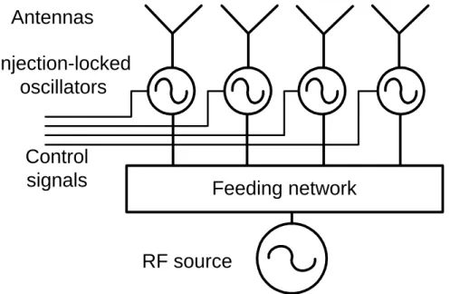
Like the traditional phased array, there are many beam-scanning schemes for the injection-locked or mutually coupled oscillator arrays. The most straightforward application of injection-locking technique to phased array is shown in Fig. 1.2 [21]. Each array element is a self-contained voltage-controlled oscillator (VCO) that delivers power to an antenna. This scheme eliminates phase shifters but suffers from limited inter-element phase difference range and the requirement of feeding networks.
A variation of this idea, which eliminates the feeding network, is cascade-coupled scanning array [22]. Figure 1.3 illustrates this scheme. In this structure, each element is slaved to the preceding element in the array. Comparing to Fig. 1.2, it enhances the scanning range, but requires additional amplifiers or isolators to implement the unilateral coupling networks.
An extension of injection-locking concept is a mutually coupled oscillator array [2]-[8]. Each oscillator element is bilaterally coupled to adjacent array elements. Mutual coherence is achieved by the injection-locking process, but the steady state phase relationships are difficult to calculate since each oscillator
depends on the phase of its neighbor. However, in certain cases, the equations can be linearized and solved to produce the phase progressions required for beam scanning. This has led to some interesting approaches.
The system of a mutually coupled oscillator array is illustrated in figure 1.4. There are different ways to produce progressive phase distribution for this array. Stephan’s array uses external signals injected at the opposite ends of the array [23]. The phase difference between the two injection signals is divided uniformly along the array to produce a constant progressive phase.
Another approach to produce a constant progressive phase for a mutually coupled oscillator array is edge detuning [2]-[8], which changes free-running frequencies of the edge oscillator elements in the opposite directions. The advantage of this approach is that only periphery array elements need to be controlled.
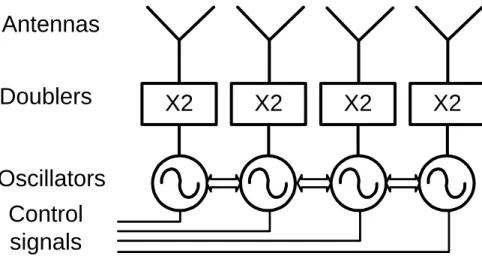
One apparent limitation of the injection-locked or coupled oscillator is the limited phase shift range that can be synthesized. This could be improved by introducing a frequency doubler after each oscillator as shown in Fig. 1.5 [24]. That effectively doubles the inter-element phase shift. Another benefit of this technique is that the oscillators can be designed at lower frequencies.
Two-dimensional mutually coupled oscillator array was studied to achieve two-dimensional beam scanning [9]-[11]. The phase control method is achieved by periphery detuning similar to that in the one-dimensional case.
1.3
Contributions
This report presents three new applications of mutually coupled oscillator arrays.
First of all, the design concept of push-push oscillators is extended to triple-push, quadruple-push and hence N-push harmonic oscillators [25] in Chapter 3. Instead of linear analysis, the design principle in this report is based on the injection-locking theory. According to the previous researches, the relative phase between coupled oscillators can be controlled by the oscillator free-running frequencies. The desired harmonic component is selected by tuning the relative phase of the coupled oscillators and the conduction angle of the voltage-clamping circuit. As the output phase-shifted signals are properly shaped and combined, the desired harmonic components are constructively added and lower-order harmonic components are suppressed. This structure can be viewed as the general case of push-push oscillators. Since the output power is combined in a passive circuit, it does not suffer from the power limit of the output device in cascade structures. In Chapter 3, this circuit structure is presented and verified experimentally in second-harmonic, third-harmonic and fourth-harmonic oscillators.
Secondly, a novel phase conjugation circuit and its application to retro-directive antennas are presented [26]-[28] in Chapter 4. The phase conjugation circuit uses a balanced circuit structure with subharmonically injection locked self-oscillating mixers (SILSOMs) oscillating at ω. In the operation, an input signal at ω/2 is converted to its conjugated signal with no
external source required for LO signal pumping, and the output signal frequency is locked at the same frequency of the input signal. The developed phase conjugation circuit is implemented with active antennas to become a retro-directive antenna array. Both the theoretical and measured results of phase conjugation and retro-directive performance are shown to be in good agreement.
Finally in Chapter 5, a two-dimensional mutually coupled oscillator array is studied for the application of a beam-scanning and polarization-agile antenna array [29], [30]. In the antenna array design, the polarization agility is considered as one of the two dimensions (or y-direction) with the other dimension (or x-direction) for beam scanning of a two-dimensional oscillator array in x-y plane.
By properly tuning the free-running frequencies of the oscillators, the array radiation direction can be scanned for the selected polarization states including linearly polarized, left-hand and right-hand circularly polarized states. Well-defined phase differences among oscillators for beam scanning and polarization agility are given by utilizing the second-harmonic signal. The performances of polarization agility and beam-scanning ability for a four-element antenna array are verified experimentally and show to have the potential for adaptive antenna array applications.
1.4
Chapter Outlines
The organization of this report is outlined as follows:
introduced. The analysis begins from the circuit model of the injection-locked oscillator. The time domain dynamics is then derived. Furthermore, the analysis is expanded to mutually coupled oscillator arrays. In addition, the basic concept of a push-push oscillator is introduced. That is the fundamental of the design of N-push oscillator in Chapter 3.
In Chapter 3, an N-push harmonic oscillator is presented. This is a new application of coupled oscillator arrays on producing a high frequency signal source. The design principle, circuit implement, and the experimental results are described in this chapter.
In Chapter 4, novel structures of phase conjugation circuits and retro-directive antenna arrays are presented. The coupled oscillator array is applied on the retro-directive antennas. First, some basics of retro-directive antennas are introduced. Followings are the design principle, circuit implement and the experiments.
In Chapter 5, a beam-scanning and polarization-agile antenna array is presented. Similarly, the coupled oscillator array is expended to be two-dimensional. This chapter contains the design principle, circuit implement, and experiments.
Antennas
Control
signals
Phase shifters
RF source
Feeding network
Antennas
Control
signals
Injection-locked
oscillators
RF source
Feeding network
Oscillators
Antennas
Control
signals
Fig. 1.3 Beam scanning using cascade-coupled oscillator array. The coupling network is unilateral.
Oscillators
Antennas
Control
signals
Fig. 1.4 Phased array using mutually coupled oscillator array. The coupling network is bilateral.
X2
Oscillators
Antennas
Control
signals
X2
X2
X2
Doublers
Fig. 1.5 Phased array using mutually coupled oscillator array with scanning-range enhanced doublers.
B
ASIC
P
RINCIPLES
In this Chapter, the basic principles mentioned in the previous chapter are illustrated. First, injection-locked oscillator theory is introduced. The time domain dynamics analysis of injection-locked oscillators is the fundamental of the coupled oscillators theory. Based on this theory, coupled oscillator arrays with linear coupling networks can be analyzed. Following, The basics of phase array using coupled oscillator arrays and the fundamentals of push-push oscillators are described briefly. These concepts and formulations will be the essentials of the applications in Chapter 3, Chapter 4 and Chapter 5.
2.1
Injection-locked Oscillators
There are a lot of theoretical models describing the behavior of injection-locked oscillators [12]-[15]. The most common used are the equivalent circuit analysis and the time domain dynamic analysis. Both of them are explained in this section. Subharmonically injection-locked oscillator [31]-[33] is the special case with the injection signal operated at the subharmonic frequency. It will also be included in this section.
2.1.1 Equivalent Circuit Model
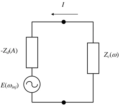
Equivalent circuit model of an injection-locked microwave oscillator was proposed by Kurokawa [14] in 1973. A microwave oscillator can be modeled as a negative resistance series (or parallel) with a load impedance near the oscillation frequency. In the injection-locking case, the injection signal can be modeled as a series voltage source (or parallel current source). The equivalent circuit of an injection-locked oscillator is shown in Fig. 2.1. -Zd(A), or the device line, is the
negative-resistance impedance of the active device. Zc(ω), or the impedance locus,
is the total circuit impedance except the active device. E(ωinj) is the injection signal.
A is the oscillating amplitude and ω is the frequency. In this model, -Zd(A) is
assumed to be only sensitive to the signal amplitude A, whereas Zc(ω) is only
related to frequency since it is a linear circuit.
[Zc(ωο)-Zd(Ao)]I= 0. (2.1)
Illustrated on the impedance plane, the free-running oscillation frequency ωo and
amplitude Ao are determined by the interception of the loci of Zc(ω) and Zd(A) as
shown in Fig. 2.2(a). In Fig. 2.2(a), these two quasi-perpendicular loci indicate that Zc(ω) is a high-Q circuit and Zd(A) primarily changes in real part.
Under the injection-locking condition, the oscillator equation becomes
[Zc(ωinj)-Zd(A)]I= E(ωinj). (2.2)
For the sake of simplicity, we do not consider the noise. The oscillating frequency is determined by the external signal. The amplitude is A as shown in Fig. 2.2(b). The length of the arrow is proportional to the amplitude of the injection signal and corresponds to the distance between the device line and the impedance locus. As the injection frequency moves away from the free-running frequency ωo, the oscillator
can not be locked by the same injection signal level. This phenomenon could also be explained by Fig. 2.2(b) with the distance of Zc(ω) and Zc(ωinj) larger than |E|/Ao.
Therefore, larger injection signal gives wider locking bandwidth.
2.1.2 Time Domain Dynamic Analysis
For an RF signal Re{Aej(ω +t φ)} with its phase φ and amplitude A slowly varying with time, its time derivative becomes
{
}
⎭ ⎬ ⎫ ⎩ ⎨ ⎧ ⎥⎦ ⎤ ⎢⎣ ⎡ + + = + + ) ( ) ( 1 ) ( Re Re jωt φ ω φ Aejωt φ dt dA A dt d j Ae dt d . (2.3)Comparing (2.3) to the time harmonic equation
{
( )} {
( )}
Re Re Aejωt+φ = jωAejωt+φ dt d , (2.4)the approximation of frequency ω is
dt dA jA dt d 1 )
(ω+ φ − . Substituting the first-order
approximation to (2.2), the equation of the injection-locked oscillator becomes
) cos( ) ( ) 1 (
Re c inj Zd A Aej( t ) E injt inj
dt dA jA dt d Z ω φ ωiinj φ = ω +φ ⎭ ⎬ ⎫ ⎩ ⎨ ⎧ ⎥ ⎦ ⎤ ⎢ ⎣ ⎡ − − + + , (2.5)
where φinj is the phase of the injection signal. Multiplying (2.5) by cos(ωinjt+φ )
and sin(ωinjt+φ ) in turn and integrating the results over the period of one RF cycle
give ) cos( ) ( ) 1 ( Re c inj Zd A A E inj dt dA jA dt d Z ω φ = φ−φ ⎭ ⎬ ⎫ ⎩ ⎨ ⎧ − − + , (2.6a) ) sin( ) ( ) 1 ( Im c inj Zd A A E inj dt dA jA dt d Z ω φ = φ−φ ⎭ ⎬ ⎫ ⎩ ⎨ ⎧ − − + − . (2.6b)
If Zc(ω) is approximated by a series resonant circuit model as
L a a L a c R R j L R R C L j Z ( )= ( − 1 )+ + ≅2 (ω−ω ) + + ω ω ω , (2.7)
ωa is the resonant frequency. (2.6a) and (2.6b) are reduced to
{
( )}
cos( ) 2 Ra RL Rd A A E inj dt dA L + + − = φ−φ , (2.8a) ) sin( 2 ) ( ) ( 2 inj a d A E inj dt d L A X L ω ω φ = φ −φ ⎭ ⎬ ⎫ ⎩ ⎨ ⎧− − − − . (2.8b)Substituting (2.7) into (2.1), the oscillator equation at free-running condition is modified as 0 ) ( ) ( 2L ωo −ωa +Xd Ao = , (2.9a) 0 ) ( = − + L d o a R R A R . (2.9b)
When the injection signal is small, A is expected to stay near the free-running value Ao. That can further reduce (2.8b) to
) sin( 2 ) ( ) sin( 2 ) ( inj o o inj inj o inj o inj o Q A A L A E dt dφ ω ω φ φ ω ω ω φ φ − − − = − − − = , (2.10)
where Ainj is the amplitude of the injection signal, and Q is the quality factor of the
resonator. This is the famous equation derived by Adler [13] in 1946 for triode oscillators and subsequently discussed in many researches. The advantage of Adler’s equation is its simplicity. Under the injection-locking condition, the locking bandwidth is given by Q A A o o inj 2 ω ω = ∆ . (2.11)
frequency Ω=(ωo-ωinj)/∆ω is defined as the frequency detuning parameter.
Adler’s equation discusses the phase relation between the injection signal and the oscillating output signal within the locking bandwidth. In this equation, the injection signal amplitude only affects the locking bandwidth, and the oscillating signal amplitude is a constant, since it is assumed to be near the free-running value. The block diagram of an injection-locked oscillator and the phase relation between the injection signal and the oscillating signal are shown in Fig. 2.3. The oscillating signal leads the injection signal with a positive frequency detuning parameter or lags the injection signal with a negative frequency detuning parameter. The maximum phase difference is ±90°. Outside the locking bandwidth, the oscillator is unstable.
Due to the small injection power required compared to the oscillator output power, injection-locked oscillators can also operate as amplifiers [34]-[36].
2.1.3 Subharmonic and Harmonic Injection
In the previous sections, only the case with injection signal at fundamental frequency is discussed. However, a nonlinear oscillator can be synchronized by either the subharmonic or the harmonic signal [31]-[33]. The injection signal then interacts with the oscillating signal in their harmonic relation. The subharmonic injection-locking phenomenon is similar to the fundamental injection locking, except the smaller locking bandwidth.
2.2
Coupled Oscillator Array
Quasi-optical oscillator arrays offer a technique for producing higher output power at millimeter wave frequency with better efficiency. There are several types of arrays that have been developed for power-combining [1]-[8].
As multiple oscillators are coupled together, from each element’s point of view, the coupling signals from the other oscillators are the injection signals. That can therefore be analyzed as an injection-locking problem.
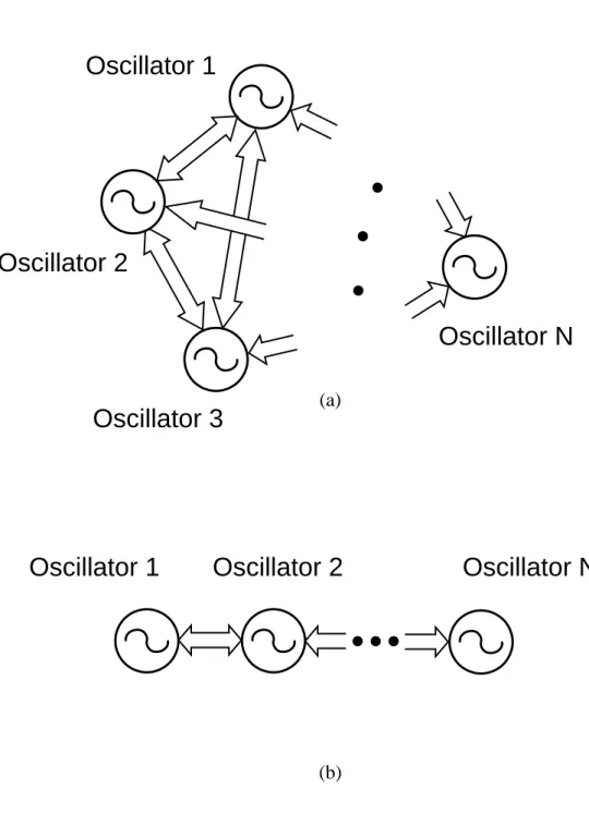
Considering an N-element coupled oscillator array shown in Fig. 2.4(a), each oscillator element is affected by all the other oscillator elements in the array. Following the dynamic analysis described in section 2.1.2, the dynamic equations for amplitude and phase of each oscillator are determined as [37]-[39]
(
)
∑
= Φ + − + − = N j ij j i j ij i o i i i o i o i A Q A A A Q dt dA 1 , 2 2 , , ) cos( 2 2 ε θ θ ω µω , (2.12a)∑
= Φ + − − = N j ij j i j ij i i o i o i A QA dt d 1 , , sin( ) 2 ε θ θ ω ω θ , (2.12b)where Ai, θi, ωo,i, Q and µ are the amplitude, phase, free-running frequency, Q- and
µ- factor of the i-th oscillator element, respectively. εij and Φij are the coupling
parameters between the i-th and the j-th oscillator elements. Similarly, the noise effect is not considered.
2.2.1 Nearest-neighbor Coupling Condition
The dynamic equations derived in the previous section describe the general condition. It becomes complicated as the array size is large. In practice, the oscillator array is usually operated under the nearest-neighbor coupling condition [37]. In this case, each oscillator element is only affected by the adjacent elements, and the coupling signals are assumed to be much smaller than the oscillating signal. It then simplifies the problem, and makes the oscillator array easy to control. An N-element oscillator array under the nearest-neighbor coupling condition is shown in Fig. 2.4(b).
As the coupling effect is weak, the amplitudes are maintain near their free-running values. Only the phase terms in (2.12b) are concerned here, since the coupled oscillator array becomes versatile under phase control. The phase dynamic equations for the oscillator array under the nearest-neighbor coupling condition are
[
]
⎪ ⎪ ⎪ ⎪ ⎩ ⎪⎪ ⎪ ⎪ ⎨ ⎧ Φ + − − − = Φ + − + Φ + − − − = Φ + − − − = − − − − sin( ) 2 ) sin( ) sin( 2 ) sin( 2 , 1 1 1 , 1 , , 32 3 2 3 32 12 1 2 1 12 2 2 , 2 , 2 21 2 1 2 21 1 1 , 1 , 1 N N N N N N N N N o N o N o o o o A QA dt d A A QA dt d A QA dt d θ θ ε ω ω ω θ θ θ ε θ θ ε ω ω ω θ θ θ ε ω ω ω θ M , (2.13)2.2.2 Phase Array Using Coupled Oscillator Arrays
Beam-scanning antenna system plays an essential role for microwave radar, imaging, and communication applications. Comparing to the conventional phased array, mutually coupled oscillator array technique is an effective approach to yield the desired aperture phase distribution without phase shifters [16]-[19]. The block diagram of a beam-scanning antenna array using coupled oscillator array is shown in Fig. 1.4. The operation of phase control is based on the injection-locking theory of oscillators.
To achieve a constant progressive phase distribution as φ
φ
φi − i−1 =∆ , (2.14)
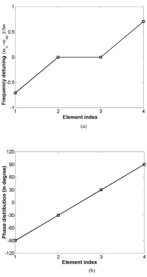
along the array elements, one can detune the free-running frequencies of the edged oscillator elements in a coupled oscillator array operated in the nearest-neighbor coupling condition as ⎪ ⎩ ⎪ ⎨ ⎧ = ∆ ∆ − < < = ∆ ∆ + = N i N i i o o o i o if , sin 1 if , 1 if , sin , φ ω ω ω φ ω ω ω . (2.15)
Figures 2.5(a) and (b) show the frequency detuning and its corresponding phase distribution of a four-element coupled oscillator array calculated based on (2.13).
The edged detuning method can also be applied to a two-dimensional coupled oscillator array under the nearest-neighbor coupling condition as shown in Fig. 2.6. A constant progressive phase distribution in a two-dimensional plane can
be produced by properly detuning the edged oscillator elements similar to the method for the one-dimensional case [9]-[11].
2.3
Harmonic Oscillator
For radar systems, microwave and millimeter-wave communications, higher frequency signal sources are required in pace with the constantly increased data rates. There are two main approaches to produce high frequency signal source. One is to design an oscillator with high fundamental frequency. Another is to design a harmonic oscillator.
At millimeter-wave, fundamental oscillators suffer from low Q-factor, insufficient device gain and higher phase noise. For harmonic oscillators, since the oscillators are operated at lower frequency, the characteristics of high Q-factor, high device gain and low phase noise become more reachable. Furthermore, the output frequency can even excess the device maximum oscillating frequency fmax [40].
2.3.1 Circuit Topologies
There are two major structures for harmonic oscillators, cascade structure and parallel structure. Taking the second-harmonic oscillator as an example, oscillator-doubler topology is the cascade structure and push-push oscillator [41]-[43] utilizes parallel structure. The circuit diagrams are illustrated in Figs. 2.7 (a) and (b), respectively. Both of them are widely used to generate the signal at the
frequency at the double of fundamental oscillation frequency. Although they share the same advantage mentioned above, push-push oscillator has less functional blocks such as frequency doubler and filter. This leads to a compact circuit size. Additionally, the output signals from two oscillators are combined in a passive circuit without suffering from the power limit of the output device in the frequency doubler.
2.3.2 Push-push Oscillator
In a push-push oscillator shown in Fig. 2.7 (b), two identical oscillators are arranged anti-symmetrically. By combing the two out-of-phase oscillation signals, the fundamental frequency components are suppressed, and the second-harmonic components are added constructively.
In the following three chapters, detail descriptions of three applications of mutually coupled oscillator array based on the injection-locking theory will be presented.
I
-Z
d(A)
Z
c(
ω
)
E(
ω
inj)
(A
o,
ω
o)
Z
d(A)
Im{Z}
Z
c(
ω
)
Re{Z}
(a)ω
inj|E|/A
oA
Z
d(A)
Im{Z}
Z
c(
ω
)
Re{Z}
(b)Fig. 2.2 (a) Impedance locus and device line for a free-running oscillator. (b) Relation between the injection signals, impedance locus, and device line.
Controlled signal
of free-running freq.
Oscillating
output signal
Injection signal
oω
) ( injt inj j inje
A
ω +φ ) (ω t+φ j injAe
(a) (b)Fig. 2.3 (a) Injection-locked oscillator. (b) Phase relation between the injection signal and the oscillating signal.
(a)
Oscillator N
Oscillator 2
Oscillator 1
Oscillator 3
Oscillator 1
Oscillator 2
Oscillator N
(b)
Fig. 2.4 Mutually coupled oscillator array under (a) general condition, and (b) nearest-neighbor coupling condition.
(a)
(b)
Fig. 2.5 Simulation results of (a) frequency detuning and (b) its corresponded phase distribution of a four-element mutually coupled oscillator array.
Osc (1,1)
Control signals Osc (2,1)
Osc (N,1)
Osc (1,3) Osc (1,N)
Frequency
doubler
Oscillator
Filter
X2
(a)Oscillator
Coupling
Oscillator
Power
combiner
(b)Fig. 2.7 Second-harmonic oscillator in (a) cascade structure, and (b) parallel structure (push-push oscillator).
N
-
P
USH
H
ARMONIC
O
SCILLATOR
In this chapter, the structure of a push-push harmonic oscillator is extended to an Nth-harmonic oscillator. For an Nth-harmonic oscillator, N oscillators with proper phase relation are arranged in parallel. The relative phases among the signal paths are controlled by a coupling network to the oscillator free-running frequencies. As these phase-shifted signals are properly combined, the desired harmonic components are constructively added and lower-order harmonic components are suppressed. In addition, the desired nonlinear effect is enhanced by the voltage-clamping circuits. Since the output power is combined in a passive circuit, it does not suffer from the power limit of the output device in the cascade
structure. This structure can be viewed as the general case of the push-push oscillator, and is presented and verified experimentally in second-harmonic, third-harmonic and fourth-harmonic oscillators. Following, the analysis method, design principle, and experimental results are presented.
3.1
Design
3.1.1 Analysis
Method
Triple-push oscillator in [44] was reported by describing the three identical oscillators operated with one even mode and two odd modes. In this section, the coupling phenomenon among oscillators is analyzed by the nonlinear injection-locking theory [13]-[15] rather than the linear mode analysis given in [44]. From this point of view, the relative phase is controlled by tuning the oscillator free-running frequencies instead of by suppressing or enhancing the three linear modes using impedance analysis.
3.1.2 Design
Philosophy
The operation of the proposed Nth-harmonic oscillator is illustrated in Fig. 3.1. For an Nth-harmonic oscillator, an array of N-element coupled oscillators is used to produce N duplicates of oscillation signals with 360°/N phase difference
between adjacent elements.
Following the oscillator in each path, a voltage-clamping circuit is used to control the conduction angle of the output signal. Comparing to the conventional push-push oscillator, which only utilizes the harmonic component in the oscillation signal, this voltage-clamping circuit can enhance the nonlinear effect. The optimum clamping voltage depends on which harmonic is desired [45]. Usually, the voltage-clamping circuit is operated as a class C amplifier (or class B for the second-harmonic oscillator). Another advantage of the voltage-clamping circuit is that the transistor operated as a class C amplifier is closed to a unilateral two-port network. Therefore, the output power combining circuit and inter-stage matching circuits can be designed independently. The pulling effect is also reduced due to the isolation between the load and the oscillators.
3.1.3 Nonlinear
Frequency
Conversion
To illustrate the scheme for the nonlinear frequency conversion, let us consider a rectified cosine wave with duty cycle to/T, which is similar to the
oscillation signal after the voltage-clamping circuit. to is the conduction time and
T is the period of the fundamental signal. If one lets t=0 be the point where the current is maximum, the Fourier-series representation of the drain current is
L + +
+ +
= cos( ) cos(2 ) cos(3 ) )
(t I I1 t I2 t I3 t
Id o ωo ωo ωo , (3.1)
The nth-harmonic current component In is [45] 2 max ) / 2 ( 1 ) / cos( 4 T nt T t n T t I I o o o n = − π π , when n≧1, (3.2)
and the DC current component is
T t I I o o π 2 max = . (3.3)
The relation between the duty cycle (or the conduction angle) and the current component is shown in Fig. 3.2. With the same output bias voltage, the maximum output power of the nth-harmonic signal delivering to the optimum power load is proportional to 1/n.
3.1.4 Power
Combining
While combining the time-shifted output signals from the N signal paths, the desired harmonic components are added constructively and the lower-order harmonic components are suppressed due to the symmetry of the signal phases. Taking the third-harmonic signal as an example, the typical phasor diagrams are shown in Fig. 3.3. With 120° phase shift among three oscillators, only the third-harmonic signals are combined in-phase. The fundamental and the second-harmonic signals are suppressed due to the symmetry in phase relation. The relation between the duty cycle and the total current component (n-path) is shown in Fig. 3.4. The maximum output power of the Nth-harmonic oscillator shown in
Fig. 3.1 is , max 2 ) / 2 ( 1 ) / cos( 4 T Nt T t N T Nt I I o o o total N = − π π , (3.4)
which is nearly independent of N.
Actually, some problems arise from this attempt to achieve a short conduction period. One is the possible breakdown occurring between the gate and drain terminals. Another is that the high input power required to achieve such a wide gate-voltage variation may deteriorate the conversion gain of frequency multiplying. According to Fig. 3.1, the power levels at the inputs of the voltage-clamping circuits are determined by the oscillators, the conversion gain directly affects the harmonic output powers. Thus, it is necessary in most cases, especially with N≧2, to uses a value of to/T greater than the optimum value.
Selecting to/T to achieve an acceptable trade-off between gain and output power is
an important part of the design process.
3.1.5 Phase
Control
For push-push oscillators, anti-symmetric phase between the two oscillators is easy to achieve. Some of them are achieved by using dielectric resonators (DR) [41]. As N>2, the phase control should be treated as a nonlinearly coupled oscillators problem. For example, in a third-harmonic oscillator, practically, these three oscillators are not identical, and the relation of oscillation signals does not
follow Fig. 3.3 while the DC power is turned on. Instead, the relative phases are tuned to the desired situation in Fig. 3.3 based on the injection-locking theory.
3.1.6 Phase
noise
According to [37]-[39], the total phase noise of the N coupled oscillators can be lowered by 1/N under the proper coupling condition. After multiplied by the harmonic relation, the phase noise of the harmonic output signal becomes degraded by a factor N as that of the fundamental signal of a single oscillator. With a stable reference signal, the harmonic oscillator can operate at injection-locked mode. The phase noise is then determined by the reference signal in this condition.
3.2
Circuit Implementation
The schematic circuit diagram of the proposed Nth-harmonic oscillator is shown in Fig. 3.5. In this chapter, second-harmonic, third-harmonic and fourth-harmonic oscillators are presented.
NE32684A HEMT devices are used for the oscillators and voltage-clamping circuits in a 1mm thick FR4 substrate. In the oscillator design, series feedback at transistor source terminal is used to produce negative resistance for oscillation. A short stub provides a DC return path, and an open stub makes the source terminal in series with desired impedance. The oscillators are biased at VGG=-0.3V and
frequency. The coupling network is implemented by transmission lines terminated with resistors, and is arranged in a ring structure to give symmetry for the end elements. In addition, the common-source class C (or class B) amplifiers are utilized in the design of voltage-clamping circuit.
3.3
Results
Since the harmonic oscillator structure proposed is general for any order of the harmonic signals, In this chapter, the second-harmonic, third-harmonic and fourth-harmonic oscillators are demonstrated experimentally.
Figure 3.6 shows the measured output spectrum of a second-harmonic oscillator. The clamping voltage is –0.7 V, which is closed to the class B operation. With 3dBm oscillator output power, the second-harmonic signal level is 5.67 dBm, and the fundamental signal level is –36.88 dBm, about 42 dB lower.
Using three-element oscillator array and three-way power combining circuit, Fig. 3.7 shows the measured output spectrum of a third-harmonic oscillator. The clamping voltage is –0.95 V. The third-harmonic signal level is –10.83 dBm, and the fundamental signal level is –25.67 dBm, which is about 15 dB lower than the third-harmonic signal level. The second-harmonic component is also suppressed according to Fig. 3.3.
Similarly, using four-element oscillator array and four-way power combining circuit, Fig. 3.8 shows the measured output spectrum of a
fourth-harmonic oscillator. The clamping voltage is –1.1 V. The fourth-harmonic signal level is –10.83 dBm, and all the fundamental, the second-harmonic and the third-harmonic signal level are lower than –25 dBm.
The result of second-harmonic oscillator shows good performance with high desired signal level and suppressed fundamental signal. For the third-harmonic and fourth-harmonic oscillators, although the output signal levels are not as high as expected, the suppression of undesired harmonic components are all about 15 dB. Several reasons cause the output power of the higher-order harmonic oscillators lower than expected as (3.4). The first one is the high loss tangent value of FR4 substrate. Secondly, as mentioned in Section 3.2, the voltage-clamping circuits are not biased at the optimum gate voltage. That lowers the desired current components. Additionally, as the transistor operated as a class-C amplifier, the effective input power from the oscillator drops dramatically as the clamping voltage rises. This results in low conversion gain of voltage-clamping circuit. Thirdly, the I-V characteristic curves of the transistor are not uniformly distributed, the smoother change near the pinch-off region neutralizes the nonlinearity of the rectified cosine signal as shown in Fig. 3.2. Finally, the lower-order harmonic suppression levels are affected by the unequal power level in each signal path. The mismatch in amplitudes from the oscillators is then enhanced by the class-C amplifiers.
3.4
Summary
quadruple-push and hence N-push oscillators, an Nth-harmonic oscillator is developed using an N-push coupled oscillator array and voltage-clamping circuits. From the injection-locking phenomenon of oscillators, relative phase between coupled oscillator array elements can be controlled by the oscillator free-running frequencies. As the phase-shifted signals are properly shaped and combined, the desired harmonic components can be combined constructively with lower-order harmonic components suppressed. This structure can be viewed as the general case of push-push oscillators. The desired harmonic component is selected by tuning the relative phase of the coupled oscillators and the conduction angles of the voltage-clamping circuits.
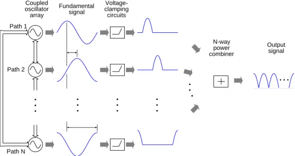
Fig. 3.1 Block diagram of an Nth-harmonic oscillator. Coupled oscillator array Voltage-clamping circuits N-way power combiner Fundamental signal Path 1 Path 2 Path N Output signal
0 0.1 0.2 0.3 0.4 0.5 0 0.1 0.2 0.3 0.4 0.5 0.6 0.7 no rm al iz e d d rai n c u rr e nt ( I/ Im a x)
duty cycle (to/T) Fundamental component
2nd harmonic component 3rd harmonic component 4th harmonic component
Fundamental
component
Third-harmonic
component
Second-harmonic
component
Path 1
Path 1
Path 2
Path 1
Path 2
Path 2
Path 3
Path 3
Path 3
0 0.1 0.2 0.3 0.4 0.5 0 0.1 0.2 0.3 0.4 0.5 0.6 0.7 no rm al iz e d d rai n c u rr e nt ( I/ Im a x)
duty cycle (to/T) Fundamental component 2nd harmonic component 3rd harmonic component 4th harmonic component
Coupling network Path 1 NE32684A VDD1 Vtune BB131 Inter-stage matching circuit Inter-stage matching circuit Inter-stage matching circuit VGG1 VDD2 Clamping voltage Path 2 Path N Power combining circuit Output
R
ETRO-DIRECTIVE
A
NTENNA
A
RRAY
In this chapter, a novel phase conjugation circuit and its application to retro-directive antennas are presented. The phase conjugation circuit uses a balanced circuit structure with subharmonically injection locked self-oscillating mixers (SILSOMs) oscillating at ωo. In the operation, an input signal at ωo/2 is
converted to its conjugated signal with no external source required for LO signal pumping, and the output signal frequency is locked at the same frequency of the input signal. The developed phase conjugation circuit is implemented with active antennas to become a retro-directive antenna array. In the following, Section 4.1
introduces the related background. Section 4.2 describes the design principles and basic formulations. Details of circuit implementation are given in Section 4.3. In Section 4.4, numerical and experimental results of a two-element phase conjugation circuit and retro-directive antenna array are presented.
4.1
Introduction
A retro-directive antenna has the unique characteristic that it retransmits incident signals backward in the direction of the sources. Although the direction of arrival techniques may have this performance [17]-[18], they may require complicated digital signal processing giving the restrictions on the high-frequency and high-speed applications. The main feature of a retro-directive antenna is to have its retransmitted signal and incident signal to be a phase conjugation pair at the microwave frequency. It can find applications in aircraft carrier landing system, automatic tolls, cargo tracking, collision avoidance, intelligent cruise control, and channel markers [16], [46]-[50].
To illustrate the basic concept of phase conjugation, an incident wave E is i expressed as
( ) j[ t (r)]
i A r e
E = ω+φ , (4.1)
where r is a position vector, ω is the angular frequency, and φ
( )
r is the position dependent phase term. Its phase-conjugated wave becomes( ) j[ t (r)]
r A r e
E = ω−φ . (4.2)
This indicates that the incident wave and its phase-conjugated wave have the same wavefronts, but propagate in opposite directions, provided that the environment is reciprocal.
One well-known retro-directive antenna structure is a heterodyne array [47]-[50] as shown in Fig. 4.1. For the n-th element, if the incident signal to the mixer is ( ), (4.3) , n t j n n i Ae v = ω +φ
and the external LO signal is at the double frequency 2ω as
= j(2ωt+θ), (4.4)
LO Ae
v
where A and θ are its amplitude and phase angle. The mixer output signal is then proportional to the conjugation of the incident signal with −φn phase term as
* , (4.5) , ) ( , , in j t j n LO n i n o cv v cA Ae cAe v v = = ω+θ−φn = θ
where c is a constant to account for the mixing product. Therefore, as the LO signal is pumped in equal amplitude and synchronized phase for each element, the retransmitted wave become phase conjugated to the incident wave.
This heterodyne array approach has been popularly applied in the areas of millimeter-wave and quasi-optics; however, it may have the following limitations. First, an external LO pumping signal is required. Secondly, it only allows single frequency operation, because the output signal frequency changes in the opposite
direction of the input signal frequency. Thirdly, its mixer needs to have good isolation between incident signal and output signal, since they are at the same frequency.
In this chapter, a novel phase conjugation circuit is presented to solve these limitations. Using a balanced circuit structure with subharmonically injection locked self-oscillating mixers, no external LO source is required and the output signal is locked at the same frequency as the input signal. With the oscillator locking characteristics, frequency modulation operation is also possible. A retro-directive antenna array is then designed by loading the proposed phase conjugation circuit with active antennas. Measurements of the bistatic retransmitted radiation pattern are conducted to illustrate its retro-directive characteristics.
4.2
Design and Formulations
4.2.1 Design
Principles
The proposed retro-directive antenna array basically uses the heterodyne array concept but with a novel design on the phase conjugation circuit to tackle the limitations of heterodyne array described in the previous section. The basic components of the phase conjugation circuit are mutually coupled subharmonically injection-locked oscillators (SILO) [31]. As the oscillator is well biased, the SILO also becomes a mixer itself due to the transistor nonlinear effect. In other words, the
oscillator behaves as a subharmonically injection-locked self-oscillating mixer. By using a balanced circuit structure with SILSOMs having in-phase coupling at the fundamental frequency, good isolation between the incident and output signals can be achieved.
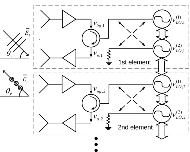
Figure 4.2 shows the basic block diagram of a retro-directive antenna element. It is constructed by using a quadrature hybrid with two SILSOMs coupled in-phase at the fundamental oscillating frequency ω [26]-[27]. This then forces two SILSOMs to oscillate coherently. The LO oscillating signals are given as
(1) = (2) = j(ωt+θ), (4.6)
LO LO
LO v A e o
v
where the superscripts (1) and (2) are used to specify the two SILSOMs. As an input signal at the subharmonic frequency ωo/2
= j(ωt/2+φ) (4.7)
inj inj A e o
v
is injected through a quadrature hybrid, the signals to the SILSOMs become
(1) ( /2 /2) 2 π φ ω + − = inj j t inj e o A v , (4.8a) (2) ( /2 ) 2 π φ ω + − = inj j t inj e o A v . (4.8b)
These two signals are then mixed with LO signals to give the output signals
. . . 2 2 ) 2 / 2 / ( 2 ) 2 / 2 / ( 1 ) 1 ( c A e c A A e hot v j t LO inj t j inj o = o + o + + − + − +φ π ω θ φ π ω , (4.9a)
. . . 2 2 ) 2 / ( 2 ) 2 / ( 1 ) 2 ( c A e c A A e hot v j t LO inj t j inj o = o + o + + − + − +φ π ω θ φ π ω , (4.9b)
where c1 and c2 are coefficients of the first-order and the second-order responses
respectively, and h.o.t. accounts for the higher-order terms.
Therefore, the output signals at the port 1 and port 2 of the quadrature hybrid are ( /2 ) . .., (4.10a) 2 1 , c A A e hot v j t LO inj port o = o + − +θ φ ω ( /2 3 /2) . .., (4.10b) 1 2 , c A e hot v j t inj port o = o + − +φ π ω
respectively. Here the separation of two signals vo,port1 and vo,port2 at the same
frequency is achieved by using the balanced circuit structure. In other words, the dominant odd-order terms (the first-order terms) are terminated at port 2, whereas the dominant even-order terms (the second-order terms) contribute to the output signal as . (4.11) * 2 1 ,port LO j inj o o v c A e v v = ≅ θ
In (4.11), it shows that the output signal is proportional to the phase conjugation of the input signal, and |c2ALO| is the conversion gain of the phase conjugation circuit.
Note (4.10a) and (4.10b) show that the good isolation of the input signal at the output (or port 2) depends on the balanced structure of quadrature hybrid.
inj
v
Loading a receiving antenna and a transmitting antenna with amplifiers at port 1 through a circulator, a basic retro-directive antenna element is constructed as
shown in Fig. 4.2. The receiving and the transmitting antennas are arranged in orthogonal polarizations to have a better isolation of input and output signals.
One can then extend the proposed structure as a one-dimensional retro-directive antenna array shown in Fig. 4.3 with all the SILSOMs coupled in-phase. For an N-element retro-directive antenna array, the output signals are given as . (4.12) ⎥ ⎥ ⎥ ⎥ ⎥ ⎦ ⎤ ⎢ ⎢ ⎢ ⎢ ⎢ ⎣ ⎡ = ⎥ ⎥ ⎥ ⎥ ⎦ ⎤ ⎢ ⎢ ⎢ ⎢ ⎣ ⎡ * , * 2 , * 1 , 2 , 2 , 1 , N inj inj inj j LO N o o o v v v e A c v v v M M θ
As shown in Fig. 4.3, an incident wave from the incident angle θ with i vertical polarization can be retransmitted back to the original direction, θr =θi, with horizontal polarization.
4.2.2 Practical
Considerations
The design equations given in (4.6)-(4.12) are derived under ideal situations. In practice, as the in-phase coupled oscillators are locked by injection signals, the oscillators are not in the same phase as (4.6) but with relative phase values among them. From [13]-[15], an injection-locked oscillator can be described by Adler’s equation as (2.10)
example for the simplicity of illustration. The injection signals for each element are ,1 ( /2 ) (4.13a) φ ω + = j t inj inj A e v ,2 ( /2 ), (4.13b) ξ φ ω + − = j t inj inj A e v
with a phase difference ξ. The injection frequency is for subharmonic injection. The four subharmonically injection-locked oscillators are under the nearest neighbor coupling condition; hence their phases should satisfy
2 / 2 / o inj ω ω ω = ≈
(
)
(
⎥ ⎥ ⎦ ⎤ ⎢ ⎢ ⎣ ⎡ − + Φ + − + Φ − ∆ = ω ω ε θ θ ε θ φ θ 2 sin sin 2 ) 1 ( 1 ) 1 ( 1 2 ) 2 ( 1 ) 1 ( 1 ) 1 ( 1 ) 2 ( 1 ) 1 ( 1 ) 1 ( 1 ) 1 ( 1 i inj i c c A A A A Q dt d)
(4.14a)(
)
(
)
(
)
⎥ ⎥ ⎦ ⎤ + − + Φ + ⎢ ⎣ ⎡ − + Φ + − + Φ − ∆ = π φ θ ε θ θ ε θ θ ε ω ω θ 2 sin sin sin 2 ) 2 ( 1 ) 2 ( 1 2 ) 1 ( 2 ) 2 ( 1 ) 2 ( 1 ) 1 ( 2 ) 1 ( 1 ) 2 ( 1 ) 2 ( 1 ) 1 ( 1 ) 2 ( 1 ) 2 ( 1 ) 2 ( 1 i inj i c c c c A A A A A A Q dt d (4.14b)(
)
(
)
(
)
⎥ ⎥ ⎦ ⎤ + − + Φ + ⎢ ⎣ ⎡ − + Φ + − + Φ − ∆ = ξ φ θ ε θ θ ε θ θ ε ω ω θ 2 2 sin sin sin 2 ) 1 ( 2 ) 1 ( 2 2 ) 2 ( 2 ) 1 ( 2 ) 1 ( 2 ) 2 ( 2 ) 2 ( 1 ) 1 ( 2 ) 1 ( 2 ) 2 ( 1 ) 1 ( 2 ) 1 ( 2 ) 1 ( 2 i inj i c c c c A A A A A A Q dt d (4.14c)(
)
(
)
⎥ ⎥ ⎦ ⎤ ⎢ ⎢ ⎣ ⎡ + + − + Φ + − + Φ − ∆ = ω ω ε θ θ ε θ φ ξ π θ 2 2 sin sin 2 ) 2 ( 2 ) 2 ( 2 2 ) 1 ( 2 ) 2 ( 2 ) 2 ( 2 ) 1 ( 2 ) 2 ( 2 ) 2 ( 2 ) 2 ( 2 i inj i c c A A A A Q dt d .(4.14d)εc and Φc are the coupling coefficient and coupling phase between SILSOMs. Φc is
designed to be zero for the in-phase coupling. εi and Φi are the coupling coefficient
subscripts specify the elements of the antenna array, while the superscripts specify the two SILSOMs in each antenna element as shown in Fig. 4.3. All the four oscillating phases are shown affected by the adjacent oscillating signals and the subharmonic injection signals. Taking (4.14a) as an example, the first term in the square bracket is the contribution of the coupling signal from , which is at the fundamental frequency. The second term in the square bracket is the contribution of the subharmonic injection signal, which is now expressed as the square of
due to the second-harmonic relation. The frequency detuning is . ) 2 ( 1 , LO v 1 , inj v inj o ω ω ω (1) 2 1 , ) 1 ( 1 = − ∆
Assuming the amplitudes and free-running frequencies of all four oscillators are the same, one can numerically solve the four mutually coupled nonlinear equations (4.14), and substitute the results into (4.6) and (4.10a). The output signals of the phase conjugation circuit are given as
. . . 2 ) 2 ( 1 ) 1 ( 1 ) 2 / ( 2 1 , hot e e e A A c v j j t j LO inj o + + = ω −φ θ θ , (4.15a) . . . 2 ) 2 ( 2 ) 1 ( 2 ) 2 / ( 2 2 , hot e e e A A c v j j t j LO inj o + + = ω −φ+ξ θ θ . (4.15b)
Here the phase distortion is assumed to be insignificant that the first-order term is negligible. Under this assumption, is approximately equal to
. Hence, (4.15) becomes 2 / ) (ejθ1(1) +ejθ1(2) ) 2 ( ) 1 ( )/2 (θ1 +θ1 j e [ /2 ( )/2], (4.16a) 2 1 , ) 2 ( 1 ) 1 ( 1 θ θ φ ω − + + = j t LO inj o c A A e v