國立交通大學
工業工程與管理學系
博士論文
利用電腦輔助設計資料防止錯打線的視覺
偵測系統之設計與開發
A CAD-based Vision Approach for Incorrect
Wire Bonding Prevention System Design and
Development
研究生﹕李恕明
指導教授﹕彭德保 博士
利用電腦輔助設計資料防止錯打線的視覺偵測系統之設計
與開發
A CAD-based Vision Approach for Incorrect Wire Bonding
Prevention System Design and Development
研 究 生:李恕明
Student: Shu-Ming Lee
指導教授:彭德保 博士
Advisor: Dr. Der-Baau Perng
國立交通大學
工業工程與管理學系
博 士 論 文
A Dissertation
Submitted to Department of Industrial Engineering and Management College of Management
National Chiao-Tung University in Partial Fulfillment of the Requirements
for the Degree of Doctor of Philosophy in Industrial Engineering and Management
July 2009
Hsinchu, Taiwan, Republic of China
摘要
在半導體封裝的製程中,沒有一種自動化的方法能在大量生產環境中正確且有效的 檢驗打線位置是否正確。本論文設計與開發了一個能預防錯打線的機器視覺系統, 利用影像處理與模擬打線的整合技術,可以在真正打線動作開始前就先檢驗打線位 置是否正確,進而避免錯打線的發生。本論文所提出的機器視覺系統不需要先製作 樣本供實際的檢驗來判斷打線位置是否正確,如此可節省製作樣本的人工、物料及 時間成本。 本論文所提出的機器視覺系統能在半導體封裝廠的大量生產環境中與生產同步 進行,不需要搬運產品至其他離線機器進行檢驗,如此可節省搬運的時間。與其他 檢驗方法比較,本論文所提出的方法可以有效的解決檢驗中常見的誤偵測與漏偵測 的問題,同時本論文也提供了一個利用電腦輔助設計資料來檢驗複雜積體電路零件 的新方向。實驗的結果顯示了此一機器視覺系統在大量生產環境中是非常完整健全 的,而且是一種能與生產速度匹配的快速檢驗方法。半導體封裝廠目前因為錯打線 而產生的不良品率約為 2000~3500 PPM [1] ,可經由本論文的方法完全改善。 關鍵字:視覺檢驗、打線位置檢查、錯打線預防Abstract
No available method can automatically verify the correctness of the wire bonding position in the mass production environment. A novel machine vision based wrong wire bonding prevention (WWBP) system is proposed that can prevent wrong wire bonding prior to actual wire bonding process execution. The proposed approach, which integrates image processing and wire bonding simulation techniques, does not need to bond actual samples for testing and can save the manual effort, material cost and product time. The proposed WWBP system can also be used to work synchronously with the real wire bonding process in the mass production environment so that the material transfer process will be reduced. This approach can efficiently solve the mal-detection and lost detection problems that may occur in other available methods. It also provides a new direction for applying CAD-based vision techniques for complicated IC parts inspection. The experimental results showed that the proposed WWBP system is robust and fast enough to work synchronously with the wire bonding process. With the proposed WWBP system, wrong wire bonding incidents, which are about 2000~3500 PPM [1] in current IC packaging foundries, will be totally eliminated.
致謝
首先要衷心感謝我的指導老師彭德保教授的諄諄教導與耐心的協助,除了在專業知識方 面的增進外,老師更啟發了學生的思維,讓我在研究態度及方法受益良多。其次感謝口試委 員清華大學工管系王茂駿教授、元智大學工工系蔡篤銘教授以及交通大學工管系巫木誠教授 與許錫美教授在論文計畫書審查與口試期間提供的寶貴意見,使這篇博士論文能更為完善。 在此致上最誠摯的謝意。 另外感謝日月光半導體股份有限公司,在研究中提供實驗用的設備、樣本以及專業的意 見與協助,使得本研究之發展得以順利完成,在此致上由衷的謝意。期間要特別感謝楊涂得 副總及許志安副總在這段期間中所給予的鼓勵、協助與包容,讓我能順利的完成學業。另外 要謝謝侯廷俊廠長及楊秀敏夫婦在論文寫作中給予的指導以及協助。 還有電腦視覺研究室的伙伴們,正全、彥仲、思翰、威廷、貴祺等同學,謝謝你們這幾 年陪我一同走過研究生涯,熱心提供寶貴的意見、鼓勵與幫助。也謝謝主內弟兄姐妹的代禱 與扶持,以及上帝一路的帶領與成就。 感謝我最親愛的父母及兄姐,當然還有我最親密的內人小美,因為有他們的支持與鼓勵, 才能讓我順利的完成博士學位,僅將此論文獻給他們,以表達我無限的謝意與愛意,祝他們 永遠的平安、建康與快樂。更願上帝的慈愛與恩惠與我所有的家人、親戚、師長、同事、朋 友同在,直到永永遠遠。 李恕明 謹致於交大工業工程與管理系電腦視覺實驗室 民國九十八年七月Contents
摘要 ... I Abstract ...II 致謝 ... III Contents ... IV List of Figures... VI List of Table ... VIII1. Introduction ... 1
1-1 Introduction to the wire bonding ...1
1-2 Objectives ...9
1-3 Scope/limitation of the dissertation ...12
1-4 Organization of the dissertation...13
2. Literature Review ... 14
3. Wrong wire bonding prevention system based on CAD drawing to inspect the wire bonding position ... 18
3-1 Image capture, process and data pre-process...20
3-2 Event monitor and remote control ...24
3-3 Bonding process simulation and wire bonding position verification ...25
4. Wrong wire bonding prevention system based on standard bonding program to inspect the wire bonding position ... 31
4-1 Image capture, process and data pre-process...31
4-2 Event monitor and remote control ...33
4-3 Bonding process simulation and wire bonding position verification ...33
5. Experimental Environment and Result ... 36
5-1 Experimental environment setting...36
5.2 Mal-detection rate and lost detection rate experimentation based on CAD drawing and using an IC with correct wire bonding...39
5.3 Mal-detection rate and lost detection rate experimentation based on CAD drawing and using an IC with wrong wire bonding...41
5.4 Mal-detection rate and lost detection rate experimentation based on SBP and using an IC with wrong wire bonding ...43
5.6 Inspection speed comparison ...50
6. Conclusions and Further Studies... 53
6-1. Conclusions...53
6-2 Contributions ...53
6-3 Further Studies...54
References ... 55
Appendix A: The leadframe design and manufacturing process... 58
Appendix B: Variation issues during wire bonding process... 64
List of Figures
Figure 1. Diagram of IC chips with bonding wires on the base material (leadframe). ... 2
Figure 2. Image of a single leadframe unit before the die is attached... 3
Figure 3. Enlarged image an illustration of a wire-bonded IC. ... 4
Figure 4. General wire bonding position setup flow in IC packaging foundries... 5
Figure 5. (a) Diagram of a wire-bonded IC. (b) An enlarged image of a part of (a). (c), (d), (e), and (f). are enlarged images of some bonding samples. ... 6
Figure 6. The ending points of the multi-layer wires are shift away the axial of the lead... 7
Figure 7. Multi-layered wire bonding (Advanced Packaging magazine, October 2005.)... 10
Figure 8. Enlarged image of multi-layered wire bonding (From http://www.kns.com). ... 11
Figure 9. Flow chart of the proposed wrong wire bonding prevention system based on CAD drawing ... 19
Figure 10. Capture leadframe image of real leadframe and leadframe layout image from CAD drawing. ... 21
Figure 11. Threshold selection for a leadframe IC image binarization... 22
Figure 12. Illustration of the calibration marks in the binarized leadframe image LIb(l). .... 23
Figure 13. Labeled the binary image LIb(l) as image LIl(l) from the top-leftmost lead clockwise. ... 24
Figure 14. Mapping the end point coordinates of WVM wires onto the imageLIl(l)... 26
Figure 15. Illustration of the shiftment of a bonding point at pad side. ... 28
Figure 16. Flow chart of the proposed wrong wire bonding prevention system based on SBP.32 Figure 17. The experimental equipment for based material image capture... 37
Figure 18. The image of the experimental base material. ... 38
Figure 19. Enlarged partial images of a sample IC used in experimentation. ...39
Figure 20. The shift distance between WVM and CAD drawing of each wire in pad side. ... 40 Figure 21. (a) Partially enlarged image of the IC with the correct bonding wire in the WVM
(before adjustment). (b) Partially enlarged image of the IC with the wire numbered
24 being bonded incorrectly in the WVM (after adjustment)... 42
Figure 22. Experimental results from inspecting a sample multi-layered wire IC. ...44
Figure 23. The shift distance between WVM and SBP of each wire in lead side and pad side. 47 Figure 24. The inspection speed comparison between manual inspection and the proposed WWBP system for the IC with different number of wires. ... 51
Figure A1. The process flow of leadframe manufacturing. ... 58
Figure A2. The inner lead is locked with polymide tape. (From : http://www.dnp.co.jp) ...59
Figure A3. The cross-section view of downset processed section. (From : http://www.dnp.co.jp) ... 60
Figure A4. A single leadframe unit before and after the cutting process. ... 60
Figure A5. Three are different etching rates at a, b, and c three regions. ... 61
Figure A6. An enlarged image of CAD drawing. ...62
Figure A7. The axial of the middle lead and the specification. ... 62
Figure A8. Over-etching of the corner... 63
Figure B1. The wire bonding position will shift away the axial from the strong light to weak light... 64
Figure B2. The platen and leadframe in the wire bond working area. (From http://www.kns.com.) ... 65
Figure B3. (a) An enlarged image of a normal leadframe-based material. (b) One lead is shifted to the right side. ... 65
Figure B4. (a) An enlarged image of a contamination in the lead. (b) An enlarged image of bad electroplating in the lead. ... 66
Figure B5. Image of wire bond working region... 67
Figure C1. Chip rotation angle of original design and WVM...68 Figure C2. The angle between any one bonding point P and the reference point P1... 70 C
List of Table
Table 1. Summary of the previous researches, available commercial systems, and the
proposed WWBP system for wire bonding position inspection. ... 17 Table 2. Lead side comparison result. In the last column on the right-hand side, “P” indicates
that the system check is passed and “F” denotes that the system check is failed...40 Table 3. Lead side comparison result after manual adjustment. In the last column on the
right-hand side, “P” indicates that the system check is passed and “F” denotes that the system check is failed... 43 Table 4. Experimental results of apply PPC method to a multi-layered wire IC with one
man-made wrong bonding wire. The lead length is 26 mils. It means that the
maximum possible shift distance of the wire is 26 mils and the bonded wire will still be on the targeted lead. In the last two columns on the right-hand side, “P” indicates that the system check is passed and “F” denotes that the system check is failed. The lead pitch is 3.7 mils, R is set to be 3.7 mils first and there are three mal-detected wires. When R is set to 11.99 mils, the mal-detection rate will be reduced. However, releasing R will also cause the lost detection problem. ... 45 Table 5. Experimental results from a multi-layered wire IC inspection with one man-made
incorrect bonding wire. The 2D image inspection method, the PPC method and the proposed WWBP system based on SBP are compared based on the mal-detection rate and lost detection rate by increasing the shift tolerance range 2 mils each time. The initial shift tolerance range is set equal to the lead pitch (3.7 mils). ... 46 Table 6. Experimental results of applying the proposed WWBP system and the PPC method
in a mass production environment. The performance indicator is focused upon the mal-detection rate. ... 50 Table 7. Comparison result of the speed of different wire bonding position check methods.... 52
1. Introduction
1-1 Introduction to the wire bonding
Wire bonding is a process that makes the connection between an IC chip and the base material. The leadframe and substrate are the two types of commonly used base materials. Bonding the wires onto the IC chip is a very critical procedure because the original connection areas of an IC chip are too small to be welded onto the PCB. Some base material is devised and used as the connecting medium between the IC chip and the PCB. Each of the connections on an IC chip is called a pad. The interval between two adjacent pads is generally referred to as a pitch. The internal connector on the base material is called a lead. Typically, a gold wire of high purity (99.99%) is used to connect the pad and corresponding lead. A bonding ball is formed on the pad, while a bonding stitch is formed on the lead. One lead may consist of more than one bonding stitch. The image of an entire chip with 216 leads and 312 surrounding wires is shown in Figure 1. The image of a single leadframe unit without the IC chip is shown in Figure 2. A part of the enlarged wire-bonded IC image is illustrated in Figure 3.
The entire set up flow for the bonding machine with the correct wire bonding positions in ordinary IC packaging foundries is composed of 5 parts, as illustrated in Figure 4, and is described below. The R&D department first generates the CAD drawing (Step 1 of Figure 4) which includes the base material layout and the bonding wires with the wire bonding positions according to the required spec, as shown in Figure 5(a). The base material factory will then fabricate the base material according the CAD drawing.
When IC packaging foundries receive the base material, the production engineers set up the first bonding machine with the correct wire bonding positions based on the given CAD drawing (Step 2 of Figure 4). In setting up the bonding machine, engineers must perform the following operations and determine the associated parameters: set up the calibration marks, the initial bonding
Figure 5. (a) Diagram of a wire-bonded IC. (b) An enlarged image of a part of (a). (c), (d), (e), and (f). are enlarged images of some bonding samples.
positions, the coordinate values of the ending point of each wire, bonding sequence of each wire, and determine the bonding parameters (such as lighting condition). The bonding positions of each wire can be set up manually or downloaded from a CAD drawing followed by converting the designed wire bonding information into the bonding program of a wire bonder [1]. Ideally, the CAD drawing download process will correctly set up the wire bonder’s bonding program. However, in practice, some bias between the CAD drawing and the base material such as “the gap of mask design” and “process variation in base material manufacturing” (Appendix A) may still exist and the set-up must be manually calibrated. Another bias is the CAD drawing is designed for easy to read, clearly be distinguished and to prevent mis-assessment due to overlap when a lead has multi-layered wires. There are gaps between the ending points of the CAD drawing and the axial of the lead, as show in Figure 6. Therefore, in the end, after the CAD drawing download process still needs manually calibrated.
Figure 6. The ending points of the multi-layer wires are shift away the axial of the lead.
After the set up, engineers will bond a sample and check the correctness of the wire bonding positions manually according to the CAD drawing with the aid of a microscope. Once a sample bonding position is found not correct, the engineer must adjust the setting, bond a new sample and repeat the checking procedure again. After the engineers have confirmed that the wire bonding positions are correct, all setting operations and parameters from the first setup machine must be
stored as the standard bonding program. The standard bonding program is then used the next time or duplicated to other bonding machines to save the setup time.
To finish each production order, IC packaging foundries need several bonding machines to work at the same time to reduce the production cycle time. The engineer duplicates the bonding program from the first setup machine into other bonding machines (Step 3 of Figure 4). In duplicating the bonding program, engineers must calibrate the bias of the wire bonding positions, for each of the other different bonding machines, such as the initial bonding positions, calibration marks, and lighting condition. After the calibration, engineers will have the set-up machine bond a sample and execute the same checking procedure as shown in the Step 2 of Figure 4 to avoid mishandling the bias calibration. After these operations, the engineers will release this bonding machine for mass production (Step 4 of Figure 4).
Even in mass production, the wire bonding positions must frequently be adjusted manually (Step 5 of Figure 4) throughout the entire bonding process. A number of products would experience variation issues during wire bonding process. The major variations include the variation from machine to machine, platen issue, lead position variation, bad or contaminated electroplating, and thermal-induced deformation or shrinkage (Appendix B). It would require continuous adjustment of wire bonding locations. But during adjustment, it is possible to result in the wrong wire bonding due to negligence. To prevent incorrect wire bonding, it is necessary to bond a new sample and check in detail after every adjustment.
Steps 2, 3 and 5 in Figure 4 are the critical procedures in setting up the wire bonding positions and might cause incorrect wire bonding. Because ICs have become increasingly more complicated, the number of wires has increased accordingly, reaching to several hundreds. For example, the number of wires in a leadframe IC can range up to 300. It takes about 2 to 3 hours for an engineer to set up the corresponding wire positions to be bonded. During the tedious wire bonding positions
setup process, it is inevitable that mistakes will be made. Incorrect wire-bonding will occur as shown in Figure 5(d).
Because wrong wire bonding is non-reworkable – cannot be repaired into correct bonding, it is a serious cost problem in the wire bonding process. Up to the present, IC packaging foundries still rely on humans to check the correctness of wire bonding positions with the aid of microscopes. Such manual inspection is prone to errors and cannot work synchronously with the bonding machines. A novel CAD-based vision approach is proposed to prevent wrong wire bonding in this dissertation. The proposed approach can be used to work synchronously with the bonding machine.
1-2 Objectives
The major objective of this dissertation is to develop an incorrect wire bonding prevention system, including the hardware and software. The hardware of the proposed system includes the illumination module, image capturing module and loading module, while the software of the proposed system includes the inspection algorithms and the hardware controlling module. This dissertation focuses on the control system and the inspection algorithm.
There are three focal points in the inspection system: (a) inspect the correctness of the wire bonding position on a multi-layered wire IC, (b) fully solve the problems of mal-detection (false positive, the wire is bonded in the correct position but is recognized as an incorrect bond) and lost detection (false negative, the wire is bonded onto the wrong lead but is recognized as a correct bonding case) that may occur in other available methods, (c) work synchronously with the wire bonding process in the mass production environment. The first focus of the proposed vision inspection system is to inspect the correctness of the wire bonding position on a multi-layered wire IC. To a multi-layer wire IC, such as that shown in Figures 7 and 8, the image of the wires in the lower layer would be hidden by the shade of the wires in the upper layer. The wires in the lower
layer cannot be observed and identified correctly by using the available 2D inspection methods. We developed a method which integrates image processing and the wire bonding position simulation technique, that can auto-inspect such correctness was first proposed. The proposed method captured the image of leadframe IC and checked the correctness of the wire bonding position before the actual bonding process was executed. There is no need to extract the wire from the complex varying background after the bonding process. Post-wire-bonding image identification is not required because such an inspection approach is based only on the information of the bonding sequence, the coordinate values of both end points of each wire and the base material image. In other words, there is no need to concern about whether the image of the wires in the lower layer will be blocked or hidden by the shadow of the wires in the upper layers. Therefore, the proposed approach can be used for inspecting the bonding position of multi-layer wire ICs.
Figure 8. Enlarged image of multi-layered wire bonding (From http://www.kns.com).
The second focus of the proposed vision inspection system is to solve the mal-detection and lost detection problems that may occur in other available methods. Compared with the other substrate-based IC product material fabricated using a mask, the leadframe-based material is fabricated by punching or etching and has the problem of high variation and low accuracy for each lead. This implies that in the punching or etching process a lead will invariably be shifted and the engineer must adjust the wire bonding positions from time to time in order to fit the variation. Figure 5(e) shows a wire bonded to a position that is slightly higher than the designed position. However, it is still bonded on the same lead and is accepted as a correct bond. For other available methods, this wire will be recognized as being incorrectly bonded and a mal-detection will occur. The mal-detection problem for the “Ground Bond” wire is the most critical because the allowable shift in the ground bond is as large as the entire ground bond area. Figure 5(f) shows a ground bond that is shifted slightly to the right but is still in the acceptable position. Another issue, electroplating quality, will also affect the leadframe quality and consequently affect the wire bonding positions.
To filter out the mal-detection or lost detection problem in the bonding position inspection, a set of associated inspection algorithms were also proposed.
The third focus of the proposed vision inspection system is to have it work synchronously with the wire bonding process in the mass production environment. In mass production environment, the wire bonding positions must frequently be adjusted manually throughout the entire bonding process. To prevent incorrect wire bonding, it is necessary to bond a new sample and check in detail after every adjustment. The proposed vision inspection system must fast enough to work synchronously with the wire bonding process.
By using the proposed image process and inspection algorithms, we can develop an AOI system to detect and prevent all the incorrectness wire bonding.
1-3 Scope/limitation of the dissertation
The proposed vision inspection system is focused on the leadframe-based material IC product. The substrate-based material IC product or other special based material IC product is not included in the study.
The defects that may occur on the bonding wire can be classified into the problems of incorrect bonding position and wrong shape of the bonding wires. The proposed vision inspection system is focused on the defect inspection of incorrect bonding position. The inspection of the wrong shapes of the bonding wires is to detect whether any wire is shifted, shorted, or sagged during the wire bonding process. It still need to rely on post-wire-bonding inspection and is not included in this study.
1-4 Organization of the dissertation
This dissertation is organized as follows. Section 2 presents a survey of the researches on wire bonding position inspection. The proposed system is described in Section 3 and Section 4. Some inspection experiments and the performance analysis of the proposed approach are presented in Section 5. Section 6 presents the conclusions and future researches.
2. Literature Review
In the wire bonding inspection process the inspectors focus on (a) the position of the bonding wire and (b) the contour and position of the bonding ball [2]. Khotanzad et al. [3-4] presented an automatic system for evaluating bonding ball quality. Sreenivasan et al. [5] presented a method to compute the bonding ball’s shape, size and location to determine its quality. All of their systems [2-5] can determine the location of the bonding ball from a 2D image of an IC wafer and extract bonding ball geometrical information. Tsukahara et al. [6] presented a vision inspection system for IC bonding wire that uses high contrast image capture and an accurate bonding-ball measurement algorithm based on sub-pixel and morphological techniques.
With the development of automatic optical inspection (AOI) technology, the IC packaging foundries attempted to improve the wire bonding position inspection using an AOI system. The AOI system has emerged as an effective inspection approach in PCB assembly [7-9], but is still not ready for wire bonding position inspection in IC packaging foundries. Ayoub [10] pointed out the AOI system problems with wire bonding position inspection. The commercial systems still need to enhance the signal to noise ratio, extend the defect coverage from single wire ICs to multi-layered wire ICs and increase the inspection speed. The ability to separate the wire from a complex varying background between the die and pad is an important aspect of post-wire-bonding inspection. Accomplishing this task requires smart illumination and inspection algorithms to work together to increase the signal-to-noise ratio between the wire and its surroundings. Wang et al. [11] presented a machine vision inspection technique with a defect detection algorithm for the bonding ball and bonding wire. Their experimental results showed that a good lighting condition can improve the recognition rate.
Ngan and Kang [12] presented an algorithm for inspecting the bonding wire. They used Hough transformation to determine the straight-line equation of the bonding wire. A fiber optic ring light was used as the light source to highlight the bonding wires. Ye et al. [13] presented an
inspection system that applied a stereo vision technique to detect the defects related to the 3D profile of bonding wires. They proposed that the illumination system should maximize the light reflected from the bonding wires and minimize the light reflected from the surface of the chip. Perng et al. [14–16] devised a vision inspection system equipped with a structured lighting system to highlight the bonding wire. Their system can be used for the on-line inspection of single layer wire ICs. In the multi-layered wire IC case, such as that shown in Figures 7 and 8, none of the existing 2D image inspection methods [2-6, 11-16] can be applied because the image of the wires in the lower layer would be hidden or shadowed by the wires in the upper layer.
Some other researchers [17-19] recovered the 3D shape using a photometric method and structured lighting system. However, multiple images are required in these researches to determine the surface normal. Kim and Koh [20] discussed the shadow problem for in-line shape inspection of LEDs using pattern projection techniques. Because of the high ratio of the outside wall to the width of the inside base area, conventional measurement techniques for projecting patterns in off-optical axis easily fail to perceive the entire shape of LEDs and produce noisy results due to the shadow problem. Kim and Koh [20] also presented a sensor system utilizes a dual projection system. Using two measurement results acquired from pattern projections switching with different incident angles, shadow-free results can be acquired. But this only resolves the shadow problem for the outside wall, not for the hidden or shadowed problem by the wires in the upper layer.
Lim et al. [21] presented an auto-focusing technique to measure the height and diameter of the bonding ball. Their method can also be used for the inspection of missing bonds and wire loop height measurements. Because a high-magnification microscope was used in their system, only the image of the wires in the focused plane could be captured clearly, while the wires in the other planes were hard to observe or inspect. KAIJO Corporation [22] used an auto-focusing technique to develop a wire bonding AOI system (WI-110). The KAIJO Corporation claimed that their system could correctly inspect multi-layered wire products. The WI-110 system searches for the bonding
ball position on the pad side first and defines it as the starting point. Next, the loop height of the wire is measured from the starting point until the ending point is found, and then converts the loop height of each point in the wire and converts this into the wire track. The auto-focusing technique inspection speed is very slow. The KAIJO machine took 8 seconds to inspect a single wire [23]. Since the available AOI machine for the wire bonding inspection is not sufficiently fast, only off-line inspection machines were adopted.
Pacheco et al. [24] presented an advanced time domain reflectometry (TDR) technique to detect the defects in multi-layered wire ICs. Only a laboratory prototype was implemented because of the high cost of this system.
Kulicke & Soffa Industries Inc. (KNS) presented a process program comparator (PPC) technique with their KNet system [25]. Image verification is not required because such an inspection approach is based only on the bonding sequence and the coordinate value of the ending point of each wire. The major drawback of the PPC method is that the PPC method does not have any actual visual inspection and does not utilize the actual lead position information. Some serious mal-detection or lost detection problems were encountered when their system was applied to a product composed of leadframe based material. Compared with the other substrate-based IC product material fabricated using a mask, the leadframe based material is fabricated by punching or etching and has the problem of high variation and low accuracy for each lead on it. Although KNS provided a fast and on-line inspection solution for multi-layered wire ICs, their method could only be applied to a product composed of substrate-based material. Until now, no commercial equipment existed that could meet all of the wire bonding position inspection requirements.
In this dissertation, a novel method is proposed to solve the wire image hidden problem for multi-layered wire ICs and eliminates the mal-detection and lost detection problems for leadframe-based material ICs. The proposed method integrates the image processing and wire bonding simulation techniques to automatically inspect the correctness of wire bonding positions.
The wire bonding position correctness is compared with the standard before the actual bonding process begins. Post-wire-bonding image identification is not required because such an inspection approach is based only on the information of the bonding sequence, the coordinate values of both end points of each wire and the base material image. In other words, there is no need to concern about whether the image of the wires in the lower layer will be blocked or hidden by the shadow of the wires in the upper layers. Therefore, the proposed approach can be used for inspecting the bonding position of multi-layer wire ICs. It uses the original CAD drawing as the comparison standard. When the CAD drawing is not available for the IC packaging foundries, the first setup machine will be used as the comparison standard.
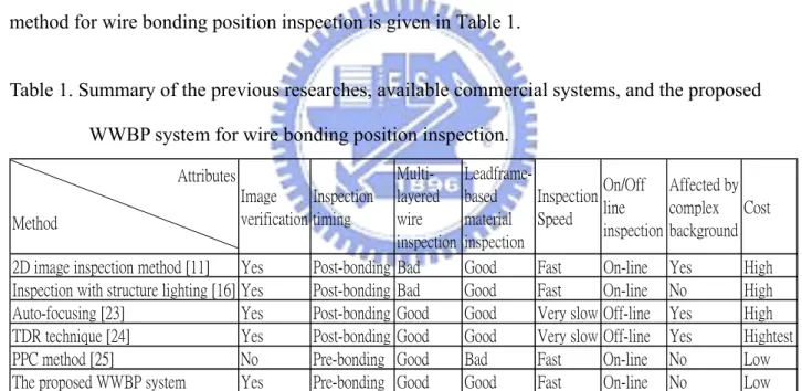
A summary of the previous researches, available commercial systems and the proposed method for wire bonding position inspection is given in Table 1.
Table 1. Summary of the previous researches, available commercial systems, and the proposed WWBP system for wire bonding position inspection.
Attributes Method
2D image inspection method [11] Yes Post-bonding Bad Good Fast On-line Yes High Inspection with structure lighting [16] Yes Post-bonding Bad Good Fast On-line No High
Auto-focusing [23] Yes Post-bonding Good Good Very slow Off-line Yes High
TDR technique [24] Yes Post-bonding Good Good Very slow Off-line Yes Hightest
PPC method [25] No Pre-bonding Good Bad Fast On-line No Low
The proposed WWBP system Yes Pre-bonding Good Good Fast On-line No Low
Image verification Inspection timing Multi-layered wire inspection Cost Leadframe-based material inspection Inspection Speed Affected by complex background On/Off line inspection
3. Wrong wire bonding prevention system based on CAD drawing to inspect
the wire bonding position
In modern bonding machines the actual wire bonding operation is triggered according to the coordinate values of the starting point (pad side) and ending point (lead side) of the bonding program. That is, when the coordinate values of the bonding program are set in the correct positions, the actual position of each wire will be bonded correctly (the bonding accuracy is about ±2.5 μm). The proposed WWBP system utilizes this advantage to simulate the actual wire bonding operations for wire bonding position verification. This approach can prevent incorrect bonding before the physical wire bonding process is executed.
The proposed WWBP system first captures the image of a single leadframe unit without IC chip or any bonding wire on it. The WWBP system then labels each lead on the image with a unique pseudo code for the later simulation process. The bonding program is obtained from the bonding machine through the SEMI SECS/GEM communication protocol. Each of the [X, Y] coordinate values for the wire bonding positions is obtained by decoding the bonding program. Based on the captured leadframe image and the coordinate values of the wire bonding positions, the WWBP system simulates a wire bonding operation for the waiting verification machine (WVM) to calculate the end point location of each wire and obtains a numbered pseudo code for each corresponding lead. The pseudo code of each lead is compared with the CAD drawing to verify whether the wires were bonded correctly.
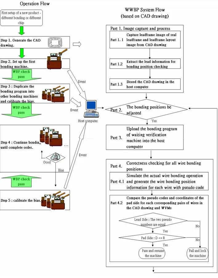
The entire WWBP system is composed of four parts, as illustrated in Figure 9, and is described in below.
3-1 Image capture, process and data pre-process
Part 1: Image capture and process.
When IC packaging foundries receive an order for a new product, different bonding or different IC chip, the R&D department will generate a CAD drawing and issue an order to the base material factory to fabricate the base material (Step 1 of Figure 4). After receiving the base material, the engineer must capture the images and process them using the following three substeps.
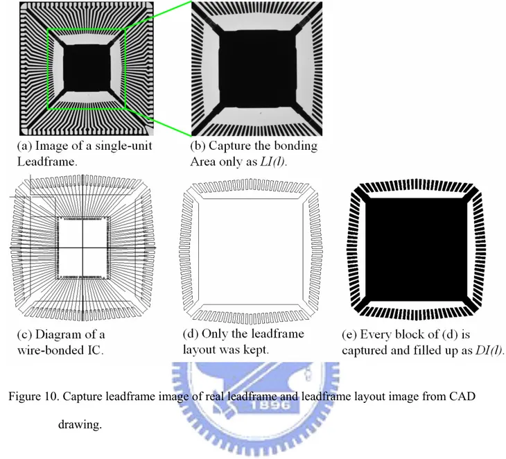
Part 1.1: Capture leadframe image of real leadframe and leadframe layout image from CAD drawing. The leadframe image is captured asLI(l) using a back light (see Figure 10(a)). Only the bonding area needs to be included in the image (see Figure 10(b)). Then, the leadframe layout image is captured from the CAD drawing and is filled up into every block of the leadframe. A full set of CAD drawings for the wire-bonded IC includes the leadframe layout and bonding wires in different drawing layers (Figure 10(c)). With the tool of AutoCAD, it is easy to keep the targeted drawing layer of leadframe only (Figure 10(d)). Every block of the leadframe is then captured and filled up into a solid as DI(l) (Figure 10(e)).
Part 1.2: Extract the lead information for bonding position checking.
Part 1.2.1: Because the gray-level histogram of LI(l) and DI(l) has a near-bimodal distribution, as shown in Figure 11, a valley-emphasis auto-threshold selection method [26] can be used to binary LI(l) and DI(l) into LIb(l) and
) (l DIb .
Figure 10. Capture leadframe image of real leadframe and leadframe layout image from CAD drawing.
Figure 11. Threshold selection for a leadframe IC image binarization.
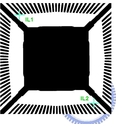
Part 1.2.2: Define the calibration marks in the image. The calibration mark is used as a reference when a leadframe is moved to the bonding area that may usually shift and rotate. Ordinarily, there are four calibration marks are used in bonding position setup, two on the lead side (leadframe) and two on the pad side (IC chip). Here we only need to define the lead side calibration marks in the image. The coordinates for the two calibration marks in LIb(l) can then be determined accordingly, say IL1(XIL1,YIL1), IL2(XIL2,YIL2) from left to
right, as shown in Figure 12. The coordinates for the two calibration marks in the image DIb(l) can then be determined accordingly, say IL1’(X'IL1,Y'IL1)
and IL2’( X'IL2,Y'IL2 ). In the later procedure, the coordinates of these
calibration marks are used as the basis to convert the coordinates of the actual bonding positions into corresponding image coordinates.
Figure 12. Illustration of the calibration marks in the binarized leadframe image LIb(l).
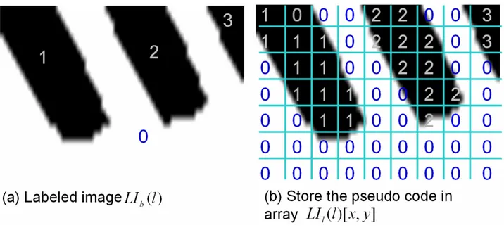
Part 1.2.3: Label each solid line (lead) on the two binary images LIb(l) and DIb(l), respectively, with a separate set of pseudo codes. The pseudo code for each lead was given starting from the top-leftmost lead, clockwise, as shown in Figure 13(a). All of the pixels of the same lead (solid line) are given the same pseudo code. The labeled images LIl(l) and DIl(l) , respectively, corresponds to the binary imageLIb(l) and DIb(l). The set of pseudo codes are stored in two 2D arrays LIl(l)[x, y] and DIl(l)[x, y], where [x, y] is the coordinate value of each pixel, as shown in Figure 13(b).
Figure 13. Labeled the binary image LIb(l) as image LIl(l) from the top-leftmost lead clockwise. Part 1.3: Stored the CAD drawing in the host computer. The engineer stored the CAD
drawing into the host computer for the later bonding position verification.
3-2 Event monitor and remote control
Part 2: The wire bonding positions be adjusted.
Once the wire bonding position was changed (Step 2, Step 3, or Step 5 of Figure 9) in a modern bonding machine, an event will be sent to the host computer via the SEMI SECS/GEM communication protocol. Part 3 will be executed automatically when the host computer receives this event.
Part 3: Upload the bonding program of waiting verification machine (WVM) into the host computer.
The WWBP system will automatically upload the bonding program from the WVM via the SEMI SECS/GEM communication protocol.
3-3 Bonding process simulation and wire bonding position verification
Part 4: Correctness checking for all wire bonding positions.
Part 4.1: Simulate the actual wire bonding operation and generate the wire bonding position information for each wire with pseudo code.
The bonding position of each wire is checked using the CAD drawing, WVM bonding program and the leadframe image. A CAD drawing/bonding program contains the bonding sequence of each wire, the coordinates of the starting point and the ending point for each wire, and the calibration mark coordinates on both the leadframe and the IC chip. The following three steps will simulate the physical/actual WVM wire bonding operation to obtain the coordinate values and pseudo codes that will be bonded onto a lead.
(a) Decode the CAD drawing/bonding program into the corresponding bonding coordinates. The CAD drawing and each type of bonding machine has its own coordinate-encoding rule. Here it is decoded by using the original encoding rule and recorded it. (b) Convert the coordinates of the actual wire bonding positions into the corresponding image coordinates. (c) Obtain the pseudo code for each wire from the labeled image.
In the case of WVMs, the XY coordinates of the end point of each wire (j) are decoded and recorded as P (l XWVM−l( j) , YWVM−l( j) ) on the lead side and
p
P (XWVM−p( j),YWVM−p( j)) on the pad side. The XY coordinates of the calibration
marks are recorded as L1 (XWVM(L1),YWVM( L1)), L2 (XWVM( L2),YWVM( L2)) on the lead
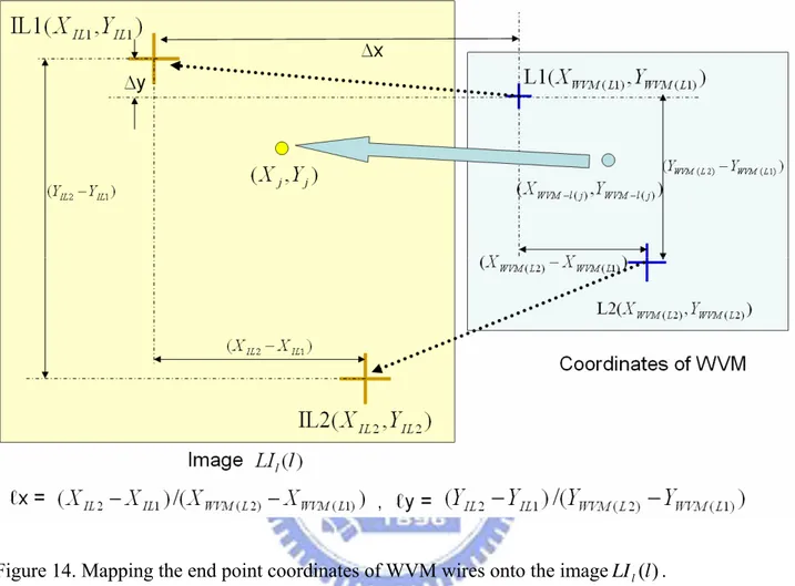
side from left to right. The end point of each wire (j) on the lead side of WVM will be mapped into the image LI (l) with the coordinate (X ,Y ) as show in Figure
14. The end point P (l XWVM−l( j),YWVM−l( j)) of a wire (j) on the lead side of the WVM
will be converted into new coordinates as follows:
Figure 14. Mapping the end point coordinates of WVM wires onto the imageLIl(l).
[X ,j Y ]= [(j XIL1 + (XWVM−l( j)–XL1) × ℓx), (YIL1 + (YWVM−l( j)–YL1) × ℓy)]
Then the pseudo code in the labeled image LIl(l) can be obtained from the 2D array LIl(l)[X ,j Y ] as j LIl(l)[(XIL1 + ( XWVM−l( j)– XL1) × ℓx), (YIL1 +
(YWVM−l( j)–YL1) × ℓy)].
Similarly, for CAD drawing, the XY coordinates of the end point of each wire (j) are decoded and recorded as 'P (l XCAD−l( j),YCAD−l( j)) on the lead side and
'
p
P (XCAD−p( j),YCAD−p( j)) on the pad side. And the ending point pseudo code of wire (j) will be obtained from the 2D array DIl(l)[X ,j Y ]. j
To provide a better bonding capability, the R&D department might design the base material in a way for the chip to be attached with a special rotation angle (see Figure 5(a)). But the actual rotation angle of the WVM is hard to keep in high accuracy with the original design. It is necessary to calibrate the rotation bias before the bonding position comparison. The algorithms are described in the Appendix C.
Part 4.2: Compare the pseudo codes and coordinates of the pad side for each corresponding pair of wires in the CAD drawing and WVMs.
One IC packaging foundry needs several bonding machines (WVMs) to work at the same time. These WVMs must be checked one by one. This part is to follow the bonding sequence to check the corresponding pair of wires of CAD and WVM. Theoretically, the starting point (pad side) and ending point (lead side) coordinates for a pair of corresponding CAD drawing and WVM wires should be equal. However, there are great variations in lead positions in the leadframe-based material. On the lead side, it is to compare the pseudo codes for a corresponding pair of CAD drawing and WVMs wires to verify whether the wire bonding positions bonded using the WVMs are correct or not. On the pad side, each point on the IC chip is practically bonded with high accuracy and low variation. The distance (D) between the CAD drawing and WVMs coordinates is then calculated. For good wire bonding it is to have the wire bonding position be controlled within a shift distance (D) which should be less than a pre-defined shift tolerance range (R). When the distance is greater than the pre-designed allowable range (R), this wire is marked as an
incorrect bond (see Figure 15). Here, R is set equal to (pad width – diameter of gold wire)/2. Then, the corresponding bonding positions of the CAD drawing and WVMs on the same pad can be guaranteed. The algorithm for the wire bonding position comparison is given below:
Figure 15. Illustration of the shiftment of a bonding point at pad side.
Algorithm: Wire bonding position comparison based on CAD drawing
Input: The pseudo code of each wire on the lead side and the XY coordinate value of every wire on the pad side
Procedure:
For j = 1 to N do /* N is the total number of to be bonded wires */
Case lead side: /* Check the bonding positions in the lead side */
If (the pseudo code for P (l' XCAD−l( j),YCAD−l( j))–the pseudo code for P (l XWVM−l( j),YWVM−l( j)) = 0)
/* Check whether the pseudo code of P (l' XCAD−l( j),YCAD−l( j)) in CAD is equal to the pseudo code of P (l XWVM−l( j),YWVM−l( j)) in the waiting verification machine.
All pixels of the same lead have the same pseudo code. The pixel of different lead owns different pseudo code. If the pseudo codes for the end points of a pair of wires in the corresponding CAD drawing and WVM are equal, then the corresponding wires in the same numbered lead can be located. */
Then the wire bonding has passed
Else the wire bonding has failed
End if
End case
Case pad side: /* Check the bonding positions in the pad side */
/* D = 2 ) ( ) ( 2 ) ( ) ( ) ( ) (XCAD−p j −XWVM−p j + YCAD−p j −YWVM−p j ;
R = Shift tolerance range */
Else the wire bonding has failed
End if
End case
End for
End procedure
After the check, the host computer will display the comparison result and go back to Part 2 waiting for the next event.
4. Wrong wire bonding prevention system based on standard bonding program
to inspect the wire bonding position
Sometimes IC packing foundries might not have the chance to take part in the design of CAD drawing and cannot get the electronic file of CAD drawing. Then the production engineers set up the first bonding machine with the correct wire bonding positions based on the hard copy of CAD drawing (Step 2 of Figure 4). The bonding positions of each wire can be set up manually into the bonding program of a wire bonder. After the set up, engineers will bond a sample and check the correctness of the wire bonding positions manually according to the hard copy of CAD drawing with the aid of a microscope. After the engineers have confirmed that the wire bonding positions are correct, all setting operations and parameters from the first setup machine must be stored as the standard bonding program. The standard bonding program (SBP) is then used the next time or duplicated to other bonding machines to save the setup time.
When the electronic file of CAD drawing is not available, the SBP will be applied for the wire bonding position inspection. The entire system is composed of five parts, as illustrated in Figure 16 and described below.
4-1 Image capture, process and data pre-process
Only the real leadframe need to be captured and processed. There is no need to process the CAD drawing. Both the SBP and the WVM’s bonding program will use the real leadframe image for simulating the bonding process.
Part 1: Image capture and process.
Part 1.1 and Part 1.2: Same procedures and rules as Part 1.1 and Part 1.2 of Chapter 3. But here only the leadframe image has to be processed, there is no need to process the CAD drawing.
Figure 16. Flow chart of the proposed wrong wire bonding prevention system based on SBP.
Part 1.3: Upload the standard bonding program into the host computer. The engineer stored the SBP into the host computer for the later bonding position verification.
4-2 Event monitor and remote control
Part 2 and Part 3: Same procedures and rules as Chapter 3.
4-3 Bonding process simulation and wire bonding position verification
Part 4: Correctness checking for all wire bonding positions.
Part 4.1: Simulate the actual wire bonding operation and generate the wire bonding position information for each wire with pseudo code.
In contrast to Part 4.1 of Chapter 3, the SBP is used to replace the CAD drawing. The bonding position of each wire is checked by using the SBP, WVM bonding program and the leadframe image.
Similarly, for SBP, the XY coordinates of the end point of each wire (j) are decoded and recorded as 'P (l XSBP−l( j) , YSBP−l( j) ) on the lead side and
'
p
P (XSBP−p( j),YSBP−p( j)) on the pad side. And the ending point pseudo code of wire (j) will be obtained from the 2D array LIl' l( )[X ,j Y ]. j
Part 4.2: Compare the pseudo codes and coordinates of the pad side for each corresponding pair of wires in the SBP and WVMs.
Similar to Part 4.2 of Chapter 3, the SBP is used to replace the CAD drawing. The algorithm for the wire bonding position comparison is given below:
Input: The pseudo code of each wire on the lead side and the XY coordinate value of every wire on the pad side
Output: The verified wire with incorrect bonding
Procedure:
For j = 1 to N do /* N is the total number of to be bonded wires */
Case lead side: /* Check the bonding positions in the lead side */
If (the pseudo code for P (l' XSBP−l( j),YSBP−l( j))–the pseudo code for
l
P (XWVM−l( j),YWVM−l( j)) = 0)
/* Check whether the pseudo code of P (l' XSBP−l( j),YSBP−l( j)) in
SBP is equal to the pseudo code of P (l XWVM−l( j),YWVM−l( j)) in
the waiting verification machine.
All pixels of the same lead have the same pseudo code. The pixel of different lead owns different pseudo code. If the pseudo codes for the end points of a pair of wires in the corresponding SBP and WVM are equal, then the corresponding wires in the same numbered lead can be located. */
Then the wire bonding has passed
Else the wire bonding has failed
End if
Case pad side: /* Check the bonding positions in the pad side */
If (D < = R) then the wire bonding has passed
/* D = 2 ) ( ) ( 2 ) ( ) ( ) ( ) (XSBP−p j −XWVM−p j + YSBP−p j −YWVM−p j ;
R = Shift tolerance range */
Else the wire bonding has failed
End if
End case
End for
End procedure
After the check, the host computer will display the comparison result and go back to Part 2 waiting for the next event.
5. Experimental Environment and Result
Three major factors are considered in the wire bonding position inspection: (a) the mal-detection rate, (b) the lost detection rate, and (c) the inspection speed, whether it is fast enough to work synchronously with bonding machines in a mass production environment. These factors are used as the performance indicators for examining the usefulness of the proposed WWBP system.
In Section 5.1, the experimental environment and samples are firstly introduced. In Section 5.2, a multi-layered wire IC chip with correct wire bonding positions is used to check the performance of the proposed WWBP system based on CAD drawing considering the mal-detection rate and lost detection rate factors. In Section 5.3, an IC chip with incorrect wire bonding positions was used, instead, to check the performance of the proposed WWBP system based on CAD drawing considering the mal-detection rate and lost detection rate factors again. In Section 5.4, a multi-layered wire IC chip is used to compare the inspection performance of the 2D image inspection method, the PPC method and the proposed WWBP system based on SBP by employing the mal-detection rate and lost detection rate. In Section 5.5, the feasibility of the proposed WWBP method when applied in a mass production environment with 145 bonding machines is discussed. In Section 5.6, the inspection speed factor for the proposed WWBP system is discussed.
5-1 Experimental environment setting
The experimental environment for wire bonding inspection is illustrated in Figure. 17. All the images of the leadframe-based material were grabbed by using a CIS VCC-880A B/W camera of 1600 x 1200 resolution and a Matrox Meteor II grabber. The inspection algorithms were programmed using Microsoft Visual Basic 6.0 and Matrox MIL 6.0. The experimental computer was powered by an Intel Celeron 1.6G CPU.
Figure 17. The experimental equipment for base material image capture.
The sample chip used in the inspection experimentation is a multi-layered wire IC chip with 216 leads. The base material of this IC chip is a Cu leadframe. The lead width, lead length, lead pitch, pad width, pad pitch and diameter of the gold wire of this IC chip, respectively, is of 4, 26, 3.7, 2.24, 0.2 and 0.9 mil. Total 312 wires including 41 ground bonds are to be bonded. Initially, the shift tolerance range R of the pad side is set equal to 0.67 mil ((pad width – diameter of gold wire)/2). Figure 18 shows the image of the experimental base material.
Figure 18. The image of the experimental base material.
Figure 19 illustrates three partially enlarged images of this sample IC. Figures 19(a) and 19(b) show that there are multi-layered wires on this IC. From Figure 19(c), it is obvious that the lead numbered 138 has 4 bonding points. Only 3 wires extending from the lead numbered 138 can be seen clearly because one wire is hidden by the wires in the upper layer. This situation will cause the mal-detection problem when the 2D image inspection method is applied even though the bond is correct.
Figure 19. Enlarged partial images of a sample IC used in experimentation.
5.2 Mal-detection rate and lost detection rate experimentation based on CAD drawing and using an IC with correct wire bonding
The engineer first selected one bonding machine as a WVM and set up the correct bonding program with detailed verification. After the engineers have confirmed that the wire bonding positions are correct, all setting operations and parameters from the WVM will be stored as the SBP for the later experimentation. The experimentation was executed using following procedure
described in Section 3. The experimental results are shown in Table 2 and Figure 20.
Table 2. Lead side comparison result. In the last column on the right-hand side, “P” indicates that the system check is passed and “F” denotes that the system check is failed.
X Y Lead Number X Y Lead Number …… 19 -86.40 241.33 16 -84.48 241.24 16 1.92 P 20 -79.00 241.89 17 -76.93 241.68 17 2.08 P 21 -57.25 246.96 20 -55.58 246.84 20 1.67 P 22 -56.34 242.56 20 -54.91 242.96 20 1.48 P 23 -50.91 162.03 55 -48.28 171.60 55 9.92 P 24 -50.32 243.79 21 -48.79 251.26 22 7.62 P 25 -50.28 247.95 21 -48.19 247.29 21 2.19 P 26 -50.44 251.91 21 -47.51 243.50 21 8.90 P …… System Result Wire Number
End point coordinates by CAD
End point coordinates
bonded by WVM Shift distance (D) 0 0.2 0.4 0.6 0.8 0 50 100 150 200 250 300 350 Wire numbered D is ta n ce ( m il)
Pad side shift distance Shift tolerance range R
Figure 20. The shift distance between WVM and CAD drawing of each wire in pad side.
Table 2 is a part of lead side comparison result. The maximum, minimum, average, and standard deviation of shift distance between the CAD drawing and WVM in lead side, respectively, is 23.68, 0.22, 3.62, and 4.49 mils. All wires were verified as correct bonding. Even the largest shift distance (23.68 mils) between WVM and CAD drawing is several times than the lead width, the
proposed system still can successfully identify this wire as a correct bonding. Figure 20 showed the pad side comparison result and all wires were identified as correct bonding (D < 0.67 mil). No any mal-detection or lost detection in the lead side or pad side inspection was encountered.
5.3 Mal-detection rate and lost detection rate experimentation based on CAD drawing and using an IC with wrong wire bonding
We can randomly select two wires (wire numbered 20 and 23 in Figure 21(a)) and adjust the wire bonding positions manually to let them shift away from the original positions in the WVM, but still retain them on the same lead (i.e., to ensure correct bonding as Figure 21(b)). Similarly, we can randomly select the other wire and adjust its wire bonding position manually to allow it to shift away from the designated bonding lead and to cause an incorrect bonding in the WVM (wire numbered 24 in Figure 21(a)).
After the adjustment was completed, the inspection system received an event from the bonding machine and was triggered to auto-inspect again (from Step 5 to Part 2 of Figure 9). The experimental results are recorded in Table 3.
A part of the image is shown in Figures 21(a) and 21(b). Comparing Figure 21(a) with Figure 21(b), we can see that even though the two wires, numbered 20 and 23, shifted away from the designated bonding position, they were still bonded onto the correct lead. The wire numbered 24 not only shifted away from the designated bonding position, but also shifted away from the designated lead. With regard to Table 3, the proposed system verified the two wires, numbered 20 and 23, as being bonded correctly. But wire numbered 24 was verified as being bonded incorrectly. Although the shift distance of the wire numbered 23 (16.32 mils) is larger than the wire numbered 24 (11.46 mils), the proposed system still successfully identified the wire numbered 23 as correct bonding and the wire numbered 24 as incorrect bonding. All wires were correctly identified. No
Figure 21. (a) Partially enlarged image of the IC with the correct bonding wire in the WVM (before adjustment). (b) Partially enlarged image of the IC with the wire numbered 24 being bonded incorrectly in the WVM (after adjustment).
Table 3. Lead side comparison result after manual adjustment. In the last column on the right-hand side, “P” indicates that the system check is passed and “F” denotes that the system check is failed. X Y Lead Number X Y Lead Number …… 19 -86.40 241.33 16 -84.48 241.24 16 1.92 P 20 -79.00 241.89 17 -79.84 252.90 17 11.05 P 21 -57.25 246.96 20 -55.58 246.84 20 1.67 P 22 -56.34 242.56 20 -54.91 242.96 20 1.48 P 23 -50.91 162.03 55 -38.68 172.84 55 16.32 P 24 -50.32 243.79 21 -41.63 251.26 22 11.46 F 25 -50.28 247.95 21 -48.19 247.29 21 2.19 P 26 -50.44 251.91 21 -47.51 243.50 21 8.90 P …… Wire Number
End point coordinates by CAD
End point coordinates
bonded by WVM Shift distance
(D)
System Result
5.4 Mal-detection rate and lost detection rate experimentation based on SBP and using an IC with wrong wire bonding
The engineers duplicate the SBP of experimentation 5.2 into other bonding machine and calibrate the bias as a WVM firstly. We can randomly select three wires (wire numbered 16, 20, and 23 in Figure 22(c) and Table 4) and adjust the wire bonding positions manually to let them shift away from the original wire bonding positions in the WVM, but still retain on the same lead (i.e., to ensure correct bonding). Similarly, we can randomly select the other wire (wire numbered 24 in Figure 22(c) and Table 4) and adjust its wire bonding position manually to allow it to shift away from the original bonding lead to cause an incorrect bond in the WVM. Initially, the shift tolerance range R of the lead side is set equal to the lead pitch (3.7 mils). The wire bonding position inspection steps were repeated as described in Section 4, by increasing the value of R by 2 mils each time when the PPC method is applied until no mal-detection can be found (see Table 5).
Table 4. Experimental results of apply PPC method to a multi-layered wire IC with one man-made wrong bonding wire. The lead length is 26 mils. It means that the maximum possible shift distance of the wire is 26 mils and the bonded wire will still be on the targeted lead. In the last two columns on the right-hand side, “P” indicates that the system check is passed and “F” denotes that the system check is failed. The lead pitch is 3.7 mils, R is set to be 3.7 mils first and there are three mal-detected wires. When R is set to 11.99 mils, the mal-detection rate will be reduced. However, releasing R will also cause the lost detection problem. X Y X Y …… 15 283.61 46.89 284.77 46.20 1.35 Y P P 16 292.84 49.91 295.77 53.37 4.53 Y F(Mal-detection) P 17 300.48 49.48 301.76 48.95 1.38 Y P P 18 307.85 48.97 309.15 48.19 1.52 Y P P 19 315.29 48.17 316.54 48.07 1.25 Y P P 20 322.88 47.95 321.24 36.08 11.99 Y F(Mal-detection) P 21 344.22 42.71 345.5 42.14 1.4 Y P P 22 344.95 46.52 346.17 46.02 1.32 Y P P 23 351.97 117.4 362.4 116.14 10.51 Y F(Mal-detection) P 24 351.01 38.1 359.45 37.72 8.45 N F P(Lost detection) 25 351.71 42.19 352.89 41.69 1.29 Y P P 26 352.32 46 353.57 45.48 1.35 Y P P …… Wire Number PPC Result for R=11.88 Shift distance (D) PPC Result for R=3.7 End point coordinates bonded by WVM End point coordinates bonded by first setup machine Bonding in the correct lead
Table 5. Experimental results from a multi-layered wire IC inspection with one man-made incorrect bonding wire. The 2D image inspection method, the PPC method and the proposed WWBP system based on SBP are compared based on the mal-detection rate and lost detection rate by increasing the shift tolerance range 2 mils each time. The initial shift tolerance range is set equal to the lead pitch (3.7 mils).
Tolerance range Inspection method Mal-detection Lost detection Mal-detection Lost detection Mal-detection Lost detection Mal-detection Lost detection Mal-detection Lost detection Mal-detection Lost detection 2D image inspection method 14 0 14 0 14 0 14 0 14 0 14 0 PPC method 3 0 2 0 2 0 2 1 1 1 0 1 WWBP system 0 0 0 0 0 0 0 0 0 0 0 0 13.7 mil
3.7 mil 5.7 mil 7.7 mil 9.7 mil 11.7 mil
The experimental results are recorded in Table 4, Table 5 and Figure 23. A part of the image is shown in Figure 22. Figure 22(a) shows the full image of the chip. Figure 22(b) is the partially enlarged image of the IC with the correct bonding wire in the first setup machine. Figure 22(c) depicts the partially enlarged image of the IC with an incorrectly bonded wire in the WVM. Figures 22(d), 22(e), and 22(f) illustrate the results from applying the PPC method. The slim lines in Figures 22(e) and 22(f) denote that these wires were verified as correctly bonded wires using the PPC method. The fat lines in Figures 22(e) (wire numbered 16, 20, 23, and 24) and 22(f) (wire numbered 20 and 23), respectively, represent the fact that they are incorrectly bonded wires. These wires were verified using the PPC method. Figures 22(g) and 22(h) are the results from applying the WWBP system. In Figure 22(h), the slim lines express the fact that the wires were verified as being correctly bonded using the WWBP system. The fat line (wire numbered 24) represents the fact that it is an incorrectly bonded wire that was verified using the WWBP system.
With regard to Table 4 and Figure 23(a), when the PPC method was applied, mal-detection occurred in the lead side. Comparing Figure 22(c) with Figure 22(e), we can see that even though the two wires numbered 20 and 23 shifted away from the designated wire bonding position, they were still bonded onto the correct lead. The PPC method verified it as being bonded incorrectly when R is 3.7 mils. The mal-detection problem could be reduced if R could be considered equal to the maximum possible D. However, releasing R might cause the lost detection problem. For example, when R was increased to 9.7 mils (Figure 22(f) and Table 5), wire number 16 is not mal-detected any more. However, the lost detection case occurred for wire number 24. Because the PPC method checks the correctness of wire bonding positions only on the basis of the shift distance, that is, since it does not have the actual information on the lead position, not all incorrect bonds can be detected. Some correct bonds may even be incorrectly detected as defective.
On the other hand, in Figures 22(g) and 22(h), as a result of applying the proposed WWBP system, no mal-detection or lost detection cases occurred. That is, despite the shade from the wires in the upper layer hiding the wires in the lower layer, as Figure 19(c) shows, the proposed WWBP system can successfully be applied for multi-layered wire IC inspection. When the WWBP system was applied, because the actual information on the lead positions was utilized, no mal-detection or lost detection occurred. All of the bonding positions for the wires can be correctly verified.
On the lead side inspection, both PPC method and WWBP system used the same algorithm. Figure 23(b) showed the pad side comparison result and all wires were identified as correct bonding (D < 0.67 mil). No any mal-detection or lost detection in the pad side inspection was encountered.
5.5 WWBP system application in a mass production environment
we implemented the proposed WWBP system and the PPC method to a production line of 145 bonding machines. There were three different models - UTC37, MaxumPlus, and MaxumUltra, of the 145 bonding machines. Any one machine of these three models was chosen randomly as a first setup machine for that model. The other machines were used as WVMs. In this experiment both the PPC method and the proposed WWBP system were executed.
There are seven different lead counts for the QFP (Quad Flat Package) product to be inspected in the production line, as given in Table 6. Each of these QFP products has several leadframe layouts. Furthermore, even the same leadframe layout for different QFP products may have several different devices (different bonding or different chips). In this experiment, we can randomly select one device from each of the same lead count products. The mal-detection rate is the performance indicator. The results of applying the proposed WWBP system and PPC method to a mass production environment are given in Table 6.
Table 6 shows that PPC method will result in mal-detection. The mal-detection rate is higher than 66%, particularly for the products with ground bonds. That is because the allowable shift tolerance range in the ground bond is as wide as the entire ground bond area (see Figure 2). Conversely, there is no mal-detection in the proposed WWBP system.