國立交通大學
電子物理學系
碩士論文
動態臨限電壓場效電晶體之
零溫度係數點模型研究
Zero Temperature Coefficient Point
Model of Dynamic Threshold
MOSFETs
研究生: 林琬琦
指導教授: 趙天生 博士
中華民國 100 年 2 月
動態臨限電壓場效電晶體之
零溫度係數點模型研究
Zero Temperature Coefficient Point Model
of Dynamic Threshold MOSFETs
研 究 生 : 林琬琦 Student : Wan-Chyi Lin
指導教授 : 趙天生 博士 Advisor : Dr. Tien-Sheng Chao
國立交通大學
電子物理學系
碩士論文
A Thesis
Submitted to Department of Electrophysics
National Chiao Tung University
In Partial Fulfillment of the Requirements
for the Degree of Master of Science
in Electrophysics
February 2011
Hsinchu, Taiwan, Republic of China.
I 動態臨限電壓場效電晶體之零溫度係數點模型研究 指導教授: 趙天生 博士 研究生: 林琬琦 國立交通大學 電子物理研究所 摘要 在本論文中,我們提供三種金氧半場效電晶體的操作模式,分別是 DT-A 模 式 ( )、DT-B 模式 ( ) 以及傳統操作模式。每種操作模式皆 搭配三種不同閘級材料,即 polysilicon、TiN 以及 TaC,用以比較不同操作模式 以及不同閘極材料對元件的性能的影響。其中,DT-B 模式搭配金屬閘極可以得 到非常優良的電性,例如:它能夠提供最佳的臨限電壓變化特性(threshold voltage roll-off)、減少汲極產生的位勢降低量(DIBL) 以及接近理想值的次臨限擺動 (subthreshold swing)。然而,在同樣的閘極條件下,DT-A 模式則能擁有最佳化的 驅動電流(drive current)。此外,在廣泛的操作溫度範圍下[223K,398K],我們進 一步地從理論及實驗層面去分探討臨限電壓、汲極產生的位勢降低量以及次臨限 擺盪對溫度的相依性。 為了能夠在低溫操作下得到較高的電流增益,我們推演出動態臨限電壓金氧半 場效電晶體的零溫度係數點(zero temperature coefficient point) 模型,並且將零溫 度係數點在線性區與飽和區的預測理論值與實驗值做比較。在這個縝密的模型分 析過程中,我們不僅考慮基板偏壓效應(body bias effect ),還修正了飽和區理想 電流公式中的次方項。因此,不論是在線性區或者飽和區,我們都得到非常小的 誤差值( )。
II
Zero Temperature Coefficient Point Model of Dynamic Threshold MOSFETs
Advisor:Dr. Tien-Sheng Chao Student:Wan-Chyi Lin
Department of Electrophysics National Chiao Tung University
Abstract
In this work, we provide three operation modes of MOSFET, respectively DT-A mode ( ), DT-B mode ( ), and normal mode, and three gate materials, namely polysilicon, TiN and TaC, to compare their performance. Although DT-B mode accompanied with metal gate shows the excellent characteristics, such as the lowest threshold voltage roll-off, better DIBL and the near ideal value of subthreshold swing, the DT-A mode counterpart exhibits the optimized drive current. Furthermore, the temperature dependence of threshold voltage, DIBL and subthreshold characteristics are investigated both theoretically and experimentally over the wide operation temperature ranges from 223K to 398K.
In addition, in order to obtain high current gain at low operation temperature, we develop a zero temperature coefficient (ZTC) point model for DTMOS to compare with experimental results in the linear and saturation regions. The analysis takes in to the consideration of body bias effect and the modification of ideal square-law condition in the saturation region to obtain very small error ( ) no matter in the linear or nonlinear region.
III 誌謝 在這個夜深人靜的失眠夜裡,讓我不禁回顧起飛逝的這兩年碩士生涯。這段類 小型社會的日子幫助我增加許多人生歷練。其中,令我最景仰,也最感謝的貴人 莫過於我的指導教授--趙天生老師。淵博的學識、廣大的胸襟以及斯文的談吐都 是我值得學習的優點。當我的研究遇到瓶頸時,老師就像那窮途末路的一盞明燈, 指引我開啟新的視野與道路。老師,由衷地謝謝您。 接下來,我要感謝佛心來的王冠迪學長。無論是碩論,或者是人生態度,他的 慈悲與善良都深深感化了我,讓我不再畏懼實驗的艱難,決定昂首闊步地發揚科 學家的研究精神。學長,此刻的我深深體會到你真的好偉大,感謝你。好人會有 好報的。再者,我要感謝這兩年的心靈導師--江宗育學長。不管是課業、人際關 係,或是各種疑難雜症,學長總是用他獨特的幽默感幫助我排解困難。真是一言 難盡的感謝。我還要感謝這兩年來帶給我歡笑與淚水,讓我嚐盡酸甜苦辣的實驗 室同仁們:郭柏儀學長、高國興學長、呂宜憲學長、林哲緯學長、吳翊鴻學長、 呂侑倫學長、廖家駿學長、顏立丞學長、林岷臻學姐、黃士安學長、葉啟瑞學長、 楊才民學長、林玉喬學姐、時璟、聿民、政昌、立盈、肉肉、添舜、芳昌、其儒… 等。感謝你們強大的包容心及忍耐力,讓我留下許多溫馨美好的回憶,以及簇繁 不及備載的經典畫面。真的很謝謝你們。 接著,我要向我的父母親--林憲堂先生以及詹玉勉女士獻上最深的謝意。感謝 你們這二十四年的養育與栽培,才成就今日的我。祝福我的母親身體健康,容光 煥發,青春永駐。 最後,我要特別感謝我的男朋友--曾信傑。因為有你的陪伴,讓我這兩年的喜 怒哀樂都不孤單;不僅徹夜陪我分析問題,還帶給我許多生活樂趣,多虧有你這 位義氣相挺的生活伴侶,讓我總是充滿活力。謝謝你。祝福你大展鴻圖,飛黃騰 達。
IV Contents Abstract (Chinese)………...……….………...Ⅰ Abstract (English)………...….…………...………. Acknowledgements (Chinese)..………...Ⅲ Contents……….…..………....Ⅳ Table Caption……….………..…………....Ⅶ Figure Caption……….………..……….Ⅶ Chapter 1 Introduction 1.1 General Backgrounds
1.1.1 High-K Dielectric/ Metal Gate……...………...………...…………1
1.1.2 Dynamic Threshold Voltage MOS (DTMOS)………..1
1.1.3 Low Temperature Operation………3
1.1.4 Zero Temperature Coefficient Point (ZTC point)………...3
1.2 Organization of the Thesis………..……..………...4
Chapter 2 Performance of DTMOS with Polysilicon and Metal Gates under Different Operation Temperatures and Body Bias Effects 2.1 Introduction 2.1.1 Backgrounds……….………5 2.1.2 Motivation……….6 2.2 Experiment 2.2.1 Device Fabrication..……….7 2.2.2 Measurement Setup...………...7 2.3 Results and Discussions
V
2.3.1 The Comparison of Performance for DTMOS with Polysilicon and Metal Gates under Different Body Bias Effects
2.3.1.1 Characteristics of Drain Current.……….8
2.3.1.2 Characteristics of Threshold Voltage………..………..9
2.3.1.3 Characteristics of Drain Induced Barrier Lowing (DIBL)…...12
2.3.1.4 Characteristics of Subthreshold Swing……….….13
2.3.2 Comparison of Performance for DTMOS under Different Operation Temperatures..……….14
2.3.3 Existence of ZTC point for DTMOS………..…15
2.4 Summary………...15
Chapter 3 The Compact Modeling of ZTC Point for DTMOS 3.1 Introduction 3.1.1 Backgrounds………...59
3.1.2 Motivation………...61
3.2 Measurement Setup...………62
3.3 Results and Discussions 3.3.1 The Drain Current Model of DTMOS………...62
3.3.2 The ZTC Point Model of DTMOS………...67
3.3.3 Parameter Extraction Setup………...72
3.3.4 The ZTC Point Measurements of DTMOS…...………...….74
3.4 Summary………...75
Chapter 4 Conclusion and Future Work 4.1 Conclusion………...99
VI
4.2 Suggestions for Future Work………..…..99
References………..……….………..……….101
VII
Table Captions Chapter 2
Table 2.1 Effective work function lists………18
Chapter 3
Table 3.1 and lists for polysilicon gate at different temperatures……….77 Table 3.2 Extracted parameters for (a) DT-NMOS and (b) DT-PMOS………88 Table 3.3 Comparison of the ZTC point between theoretical value and experimental value for (a) DT-NMOS and (b) DT-PMOS……….97 Table 3.4 Drain current at ZTC point for (a) DT-NMOS and (b) DT-PMOS………..98
Figure Caption Chapter 2
Fig. 2-1 Drain current versus gate voltage for NMOS with (a) polysilicon (b) TaC (c) TiN gate under normal, DT-A and DT-B modes. The operation temperature is fixed at 223K. ………...17 Fig. 2-2 Threshold voltage versus gate length for NMOS with (a) polysilicon (b) TaC (c) TiN gate under normal, DT-A and DT-B modes. The operation temperature is fixed at 223K………19 Fig. 2-3 High frequency C-V characteristics at 1 MHz for NMOS with (a) polysilicon (b) TaC (c) TiN gate………20 Fig. 2-4 Threshold voltage versus gate length for PMOS with (a) polysilicon (b) TaC (c) TiN gate under normal, DT-A and DT-B modes. The operation temperature is fixed at 223K………21
VIII
Fig. 2-5 High frequency C-V characteristics at 1 MHz for PMOS with (a) polysilicon (b) TaC (c) TiN gate……….22 Fig. 2-6 of polysilicon, TaC, and TiN gates over a range of operation temperatures from 298K to 398K for (a) NMOS (b) PMOS...………..23 Fig. 2-7 Threshold voltage roll-off characteristics of (a) NMOS (b) PMOS with polysilicon, TaC and TiN gate under normal, DT-A and DT-B modes, respectively. The operation temperature is fixed at 223K……….24 Fig. 2-8 DIBL versus gate length for NMOS with (a) polysilicon (b) TaC (c) TiN gate under normal, DT-A and DT-B modes. The operation temperature is fixed at 223K.25 Fig. 2-9 DIBL versus gate length for PMOS with (a) polysilicon (b) TaC (c) TiN gate under normal, DT-A and DT-B modes. The operation temperature is fixed at 223K.26 Fig. 2-10 DIBL of (a) NMOS (b) PMOS with polysilicon, TaC and TiN gate under normal, DT-A and DT-B modes, respectively. The operation temperature is fixed at 223K. ………...27 Fig. 2-11 Subthershold swing versus gate length for NMOS with (a) polysilicon (b) TaC (c) TiN gate under normal, DT-A and DT-B modes. The operation temperature is fixed at 223K………28 Fig. 2-12 Subthershold swing versus gate length for PMOS with (a) polysilicon (b) TaC (c) TiN gate under normal, DT-A and DT-B modes. The operation temperature is fixed at 223K………29 Fig. 2-13 Subthershold swing of (a) NMOS (b) PMOS with polysilicon, TaC and TiN gate under normal, DT-A and DT-B modes, respectively. The operation temperature is fixed at 223K………...……….30
IX
Fig. 2-14 Threshold voltage versus gate length for NMOS with polisilicon gate under (a) normal (b) DT-A (c) DT-B gate mode for different temperatures. The operation temperatures are fixed at 223K, 298K, 348K, and 398K, respectively………31 Fig. 2-15 Threshold voltage versus gate length for NMOS with TaC gate under (a) normal (b) DT-A (c) DT-B gate mode for different temperatures. The operation temperatures are fixed at 223K, 298K, 348K, and 398K, respectively………32 Fig. 2-16 Threshold voltage versus gate length for NMOS with TiN gate under (a) normal (b) DT-A (c) DT-B gate mode for different temperatures. The operation temperatures are fixed at 223K, 298K, 348K, and 398K, respectively………33 Fig. 2-17 Threshold voltage roll-off for NMOS with (a) polysilicon (b) TaC (c) TiN gate under normal, DT-A, DT-B gate mode for different operation temperatures. The operation temperatures are fixed at 223K, 298K, 348K, and 398K, respectively……34 Fig. 2-18 Threshold voltage versus gate length for PMOS with polisilicon gate under (a) normal (b) DT-A (c) DT-B gate mode for different temperatures. The operation temperatures are fixed at 223K, 298K, 348K, and 398K, respectively………35 Fig. 2-19 Threshold voltage versus gate length for PMOS with TaC gate under (a) normal (b) DT-A (c) DT-B gate mode for different temperatures. The operation temperatures are fixed at 223K, 298K, 348K, and 398K, respectively………36 Fig. 2-20 Threshold voltage versus gate length for PMOS with TiN gate under (a) normal (b) DT-A (c) DT-B gate mode for different temperatures. The operation temperatures are fixed at 223K, 298K, 348K, and 398K, respectively………37 Fig. 2-21 Threshold voltage roll-off for PMOS with (a) polysilicon (b) TaC (c) TiN gate under normal, DT-A, DT-B gate mode for different operation temperatures. The operation temperatures are fixed at 223K, 298K, 348K, and 398K, respectively……38
X
Fig. 2-22 DIBL versus gate length for NMOS with polisilicon gate under (a) normal (b) DT-A (c) DT-B gate mode for different temperatures. The operation temperatures are fixed at 223K, 298K, 348K, and 398K, respectively……….39 Fig. 2-23 DIBL versus gate length for NMOS with TaC gate under (a) normal (b) DT-A (c) DT-B gate mode for different temperatures. The operation temperatures are fixed at 223K, 298K, 348K, and 398K, respectively………...40 Fig. 2-24 DIBL versus gate length for NMOS with TiN gate under (a) normal (b) DT-A (c) DT-B gate mode for different temperatures. The operation temperatures are fixed at 223K, 298K, 348K, and 398K, respectively………...41 Fig. 2-25 DIBL for NMOS with (a) polysilicon (b) TaC (c) TiN gate under normal, DT-A, DT-B gate mode for different operation temperatures. The operation temperatures are fixed at 223K, 298K, 348K, and 398K, respectively………42 Fig. 2-26 DIBL versus gate length for PMOS with polisilicon gate under (a) normal (b) DT-A (c) DT-B gate mode for different temperatures. The operation temperatures are fixed at 223K, 298K, 348K, and 398K, respectively………...43 Fig. 2-27 DIBL versus gate length for PMOS with TaC gate under (a) normal (b) DT-A (c) DT-B gate mode for different temperatures. The operation temperatures are fixed at 223K, 298K, 348K, and 398K, respectively………...44 Fig. 2-28 DIBL versus gate length for PMOS with TiN gate under (a) normal (b) DT-A (c) DT-B gate mode for different temperatures. The operation temperatures are fixed at 223K, 298K, 348K, and 398K, respectively………...45 Fig. 2-29 DIBL for PMOS with (a) polysilicon (b) TaC (c) TiN gate under normal, DT-A, DT-B gate mode for different operation temperatures. The operation temperatures are fixed at 223K, 298K, 348K, and 398K, respectively………46
XI
Fig. 2-30 Subthershold swing versus gate length for NMOS with polisilicon gate under (a) normal (b) DT-A (c) DT-B gate mode for different temperatures. The operation temperatures are fixed at 223K, 298K, 348K, and 398K, respectively……47 Fig. 2-31 Subthershold swing versus gate length for NMOS with TaC gate under (a) normal (b) DT-A (c) DT-B gate mode for different temperatures. The operation temperatures are fixed at 223K, 298K, 348K, and 398K, respectively………48 Fig. 2-32 Subthershold swing versus gate length for NMOS with TiN gate under (a) normal (b) DT-A (c) DT-B gate mode for different temperatures. The operation temperatures are fixed at 223K, 298K, 348K, and 398K, respectively………49 Fig. 2-33 Subthershold swing for NMOS with (a) polysilicon (b) TaC (c) TiN gate under normal, DT-A, DT-B gate mode for different operation temperatures. The operation temperatures are fixed at 223K, 298K, 348K, and 398K, respectively……50 Fig. 2-34 Subthershold swing versus gate length for PMOS with polisilicon gate under (a) normal (b) DT-A (c) DT-B gate mode for different temperatures. The operation temperatures are fixed at 223K, 298K, 348K, and 398K, respectively……51 Fig. 2-35 Subthershold swing versus gate length for PMOS with TaC gate under (a) normal (b) DT-A (c) DT-B gate mode for different temperatures. The operation temperatures are fixed at 223K, 298K, 348K, and 398K, respectively………52 Fig. 2-36 Subthershold swing versus gate length for PMOS with TiN gate under (a) normal (b) DT-A (c) DT-B gate mode for different temperatures. The operation temperatures are fixed at 223K, 298K, 348K, and 398K, respectively………53 Fig. 2-37 Subthershold swing for PMOS with (a) polysilicon (b) TaC (c) TiN gate under normal, DT-A, DT-B gate mode for different operation temperatures. The operation temperatures are fixed at 223K, 298K, 348K, and 398K, respectively……54
XII
Fig. 2-38 Ion-Ioff characteristics of TiN gate NMOS at (a) 223K (b) 298K (c) 348K (d) 398K………...55 Fig. 2-39 Drain current versus gate voltage for TiN gate NMOS with different gate bias and different operation temperatures under (a) normal (b) DT-C mode. The sweep range of gate bias is from 0.8V to 1.4V, and the operation temperatures are fixed 298K, 348K, and 398K, respectively………..57 Fig. 2-40 Drain current versus drain voltage for TiN gate NMOS with different gate bias and different operation temperatures under (a) normal (b) DT-C mode. The sweep range of gate bias is from 0.8V to 1.4V, and the operation temperatures are fixed 298K, 348K, and 398K, respectively………..58
Chaper 3
Fig. 3-1 Equivalent circuits used to evaluate the effect of substrate bias on MOS I-V characteristics………...76 Fig. 3-2 Threshold voltage versus temperature for NMOS with (a) polysilicon (b) TaC (c) TiN gate under different body bias. The sweep range of body bias is from 0V to 0.6V………..78 Fig. 3-3 Threshold voltage versus temperature for PMOS with (a) polysilicon (b) TaC (c) TiN gate under different body bias. The sweep range of body bias is from 0V to 0.6V………..79 Fig. 3-4 Threshold voltage versus body bias for NMOS with (a) polysilicon (b) TaC (c) TiN gate for different operation temperatures. The operation temperatures are fixed 298K, 318K, 338K, 358K, and 398K, respectively……….80 Fig. 3-5 Threshold voltage versus body bias for PMOS with (a) polysilicon (b) TaC (c) TiN gate for different operation temperatures. The operation temperatures are fixed 298K, 318K, 338K, 358K, and 398K, respectively……….81
XIII
Fig. 3-6 Averaged values of minus body effect parameter versus temperature for NMOS with (a) polysilicon (b) TaC (c) TiN gate material. The sweep range of body bias is from 0V to 0.6V………82 Fig. 3-7 Averaged values of minus body effect parameter versus temperature for PMOS with (a) polysilicon (b) TaC (c) TiN gate material. The sweep range of body bias is from 0V to 0.6V………83 Fig. 3-8 Transconductance versus gate voltage for NMOS with (a) polysilicon (b) TaC (c) TiN gate under normal mode for different operation temperatures. The operation temperatures are fixed 298K, 318K, 338K, 358K, and 398K, respectively………….84 Fig. 3-9 Transconductance versus gate voltage for PMOS with (a) polysilicon (b) TaC (c) TiN gate under normal mode for different operation temperatures. The operation temperatures are fixed 298K, 318K, 338K, 358K, and 398K, respectively………….85 Fig. 3-10 Drain current versus drain voltage for NMOS with (a) polysilicon (b) TaC (c) TiN gate material under normal mode with different gate bias. The sweep range of gate bias is from 1V to 1.6V………86 Fig. 3-11 Drain current versus drain voltage for PMOS with (a) polysilicon (b) TaC (c) TiN gate material under normal mode with different gate bias. The sweep range of gate bias is from -1V to -1.6V………..…87 Fig. 3-12 Drain current versus gate voltage for DT-NMOS with (a) polysilicon (b) TaC (c) TiN gate for different operation temperatures. The operation temperatures are fixed 298K, 318K, 338K, 358K, and 398K, respectively and the applied drain voltage is 0.1V………..89 Fig. 3-13 Drain current versus gate voltage for DT-NMOS with (a) polysilicon (b) TaC (c) TiN gate for different operation temperatures. The operation temperatures are
XIV
fixed 298K, 318K, 338K, 358K, and 398K, respectively and the applied drain voltage is 1.2V………..90 Fig. 3-14 Drain current versus gate voltage for DT-PMOS with (a) polysilicon (b) TaC (c) TiN gate for different operation temperatures. The operation temperatures are fixed 298K, 318K, 338K, 358K, and 398K, respectively and the applied drain voltage is -0.1V……….91 Fig. 3-15 Drain current versus gate voltage for DT-PMOS with (a) polysilicon (b) TaC (c) TiN gate for different operation temperatures. The operation temperatures are fixed 298K, 318K, 338K, 358K, and 398K, respectively and the applied drain voltage is -1.2V……….92 Fig. 3-16 Experimental value of ZTC point versus body bias for NMOS with (a) polysilicon (b) TaC (c) TiN gate. The applied drain voltage is 0.1V………...93 Fig. 3-17 Experimental value of ZTC point versus body bias for NMOS with (a) polysilicon (b) TaC (c) TiN gate. The applied drain voltage is 1.2V………...94 Fig. 3-18 Experimental value of ZTC point versus body bias for PMOS with (a) polysilicon (b) TaC (c) TiN gate. The applied drain voltage is -0.1V………..95 Fig. 3-19 Experimental value of ZTC point versus body bias for NMOS with (a) polysilicon (b) TaC (c) TiN gate. The applied drain voltage is -1.2V………..96
1
Chapter 1 Introduction
1.1 General Background
1.1.1 High-K Dielectric/ Metal Gate
As CMOS device are scaled down, the conventional polysilicon/oxide gate stack suffers from high gate leakage current, intolerable resistive-capacitive delay, poly depletion, and Boron penetration especially for PMOS [1].
The use of high-K dielectric collocating with metal gate is becoming increasingly necessary to reduce gate leakage, poly depletion effect and gate resistivity at very thin oxide. As a result, metal gate/ high-k stacks are being heavily pursued recently, and the identification of suitable N/P metals is the most challenging task due to that the metal gates to replace n+ and p+ poly for bulk CMOS devices must have correct work functions; they have to fall within 0.2 eV of silicon conduction and valence band edges, even after a high-temperature anneal during source/drain activation [2-4].
1.1.2 Dynamic Threshold Voltage MOS (DTMOS)
During the past few years, demand for high-performance and low-power digital systems has grown rapidly. The low-power-consumption approach is intended for battery-operated applications, such as laptop and notebook computers as well as personal communication systems. While the high-performance approach is appropriate for applications such as microprocessors, power consumption is now becoming a critical parameter.
2
to the fact that in CMOS digital circuits, delivered power is proportional to the square of power supply voltage:
(eq. 1-1)
where is the power consumed by one gate, is the total switching capacitance of the gate, is the power supply voltage, and is averaged cooperating frequency of that gate.
Since reducing power supply voltage to below three times the threshold voltage will degrade circuit speed significantly, scaling of the power supply should be accompanied by threshold voltage reduction. However, the lower limit for threshold voltage is set by the amount of off-state leakage current that can be tolerated. It is seen that if standard MOSFETs are used, a lower bound for power supply voltage or a larger leakage current become inevitable.
To extend the lower bound of power supply to ultra-low voltages (0.7V and below), we propose a dynamic threshold voltage MOS (DTMOS). By shorting the gate to the body, the threshold voltage operated under the dynamic threshold (DT) mode is reduced by forward biasing of the body, so its current drive can be significantly enhanced in the on state; on the other hand, since the device exhibits normal threshold voltage in the off state, low standby power consumption is maintained. It actually improves the circuit speed without compromising the standby power consumption. Furthermore, steep subthreshold slope, high carrier mobility, and other improved electric characteristic are available in the DT transistor because gate bias is applied to the silicon body [5-7].
3
1.1.3 Low Temperature Operation
With CMOS device performance gains becoming increasingly difficult to gather as a direct profit of dimensional scaling, one suggestion for improving device performance is operation at reduced temperatures, that offers decreased junction leakage, sharper subthreshold turn-off transition, higher switching speed due to increased carrier mobility and decreased electrical resistance, and increased reliability due to exponential slow down of thermally activated processes such as diffusion, electromigration, and chemical reaction. Furthermore, low-temperature CMOS (LT-CMOS) is also unconditionally latch up-free because of the decreased bipolar gains of the parasitic transistors. According to above, LT-CMOS with sub-micrometer channel lengths offer great promise for high-density, high-performance, and reliable VLSI logic systems [8-9].
1.1.4 Zero Temperature Coefficient Point (ZTC point)
There is a growing need in a number of important industries for integrated electronics that can operate reliably for extended periods under severe environmental conditions. Among these are the automobile, the earth and space exploration (probes), the geothermal exploration, the aircraft engine, and the nuclear reactor industries. Considerable progress has been made in recent years towards characterizing silicon CMOS technologies for wide temperature range operation. Accurate analytical and experimental studies have revealed that most digital, and many analogue, VLSI circuits can be operated satisfactorily up to 250°C and beyond [10-12]. In addition, because conventional bipolar and weak inversion MOSFET derived, band gap-reference circuits are highly sensitive to leakage currents, they are useful over relatively narrow temperature ranges, and therefore inadequate for our purposes [13].
4
It is desirable to drive circuits designed for high temperature applications. It is a well established experimental fact that n and p-channel MOSFETs exhibit zero-temperature-coefficient (ZTC) points where the drain currents shows zero or very small variation with temperature in the linear and saturation regions. This criterion ensures that circuit parameters such as the offset voltage drift are less sensitive to the device matching tolerance [11-15].
1.2 Organization of the Thesis
By comparing the experimental data with theoretical concepts, we present a detailed study of the dependence of gate material and operation mode on the electric characteristics, such as threshold voltage, DIBL, and subthreshold swing, respectively. Here we will demonstrate the experimental results at 223K with excellent electrical characteristics.
Extending the above issue, we start to discuss the influence of temperature on the electric characteristics over the temperature range from 223K to 398K, and the results would encourage us to start the anticipation of ZTC point for DTMOS in the next section.
In the last part, for DTMOS, we first deduce a drain current model, and then present the analytical and experimental investigations of the ZTC point in the linear and saturation regions. We take into accounts of the parameters which depend on temperature, such as threshold voltage, mobility, and the body effects for the analysis; moreover, here show a series steps to extract those parameters. Finally we compare and analyze the ZTC bias values extracted from the theory and experimental results respectively.
5
Chapter 2
Performance of DTMOS with Polysilicon and Metal Gates under Different Operation Temperatures and Body Bias Effects
2.1 Introduction
2.1.1 Backgrounds
Among many metal gate materials, TiN is a very attractive candidate of mid-gap materials because of its excellent thermal stability, low resistivity and high CMOS-process compatibility [16-17]; also, TaC has been reported as a promising n-type material. On the other hand, speaking of high-k materials, Hf-based materials are more likely to be introduced in high-K/ metal gate application due to their good stability and compatibility with the conventional polysilicon gate process [2-3]. According to above, we will discuss the device characteristic issues of three different gate materials such as polysilicon, TaC, and TiN with HfSiON, respectively.
As to operation mode, even if DTMOS has big superiority, unfortunately, this device has a main drawback that the leakage current of the forward-biased p-n junction at the source fatally increases while [5][7]. Therefore, the supplied voltage must be limited to make eq. 2-1 be tenable as shown as following:
(eq. 2-1)
As a result, the validation range of could be expressed as following:
6
As is fixed, low value of would result in low , which prevents the DTMOS from enjoying a large threshold voltage reduction in on-state, and thus minimizes the current gain, but that actually could increase its upper limit of . As a result, there are three operation modes existing, respectively DT-A mode ( ), DT-B mode ( ), and normal mode ( ), to discuss the trade-off between threshold voltage reduction and upper limit of gate voltage.
Reference to operation environment temperature, although the operation at low temperature brings about many preferential benefits, while the temperature approaching absolute zero, silicon FET’s would exhibit freezeout of mobile carriers in nondegenerate substrates [9]; furthermore, below 200 K, the relationship between the inverse mobility and the vertical field for n-channel devices is modified presumably due to the change of the scattering mechanism, and the traditional deduction of mobility has not been suitable anymore [18]. Therefore, we lower the operation temperature only to 223K to avoid the freeseout problem and additional scattering mechanisms, and then freely enjoy the mentioned benefits from low temperature operation.
2.1.2 Motivation
According to above, high-K/ metal gate arranging in pairs DT-operation at low temperature may obtain very excellent current gain, especially when the applied gate bias surpasses the ZTC point bias. We will compare the fit and unfit quality of polysilicon and metal gates, and simultaneously discuss those advantages and disadvantages of normal and DT modes to figure out the trade-off.
7
2.2 Experiment
2.2.1Device fabrication
All transistors used in this work were fabricated by state-of-the-art 300 mm wafer foundry technology. HfSiO with Hf/(Hf+Si) ratio of 50% was annealing under . The high-K and 100 metal films were deposited by atomic-layer deposition (ALD) with 40 cycles and physical vapor deposition (PVD) techniques, respectively, followed by a 1000 polysilicon cap layer. In addition, before deposited the high-K dielectric, the chemical oxide was used as the interfacial layer. After gate patterning, halo implantation was used to optimize the short channel control. Eventually, a high-temperature annealing during source/drain activation and BEOL followed.
2.2.2Measurement setup
First, we set three operation modes, namely DT-A mode ( ), DT-B mode ( ), and normal mode ( ). Here, the threshold voltage is defined by constant current method [ = 40( ) nA] which painstakingly makes drain current independent of device geometry, and the measurement is simple with only one voltage measurement necessary.
In addition, the definition of drain induced barrier lowing (DIBL) and subthreshold swing (SS) are as following:
(def. 2-1) and (def. 2-2)
8
We would extract DIBL and subthreshold swing from curves measured by Keithley 4200 semiconductor parameter analyzer over wide operation temperature ranges from 223K to 398K.
Finally, CV characteristics are measured at a frequency of 1MHz with different metal gate devices to extract the equivalent oxide thicknesses and discuss the gate control capability.
2.3 Results and Discussions
2.3.1 The Comparison of Performance for DTMOS with Polysilicon and Metal Gates under Different Body Bias Effects
2.3.1.1 Characteristics of Drain Current
Fig. 2-1 shows the characteristics of with polysilicon, TaC, and TiN gates under DT-mode, respectively. In DT-mode with connecting gate to bulk together, due to the threshold voltage is a function of , the higher would reduce the body charge and thus the threshold voltage.
The reduction of body charge would lead to a lower effective normal field in the device and bring on the higher carrier mobility. The normal field could be expressed as following:
(eq. 2-3)
In addition, the net result of threshold voltage reduction is effective to increase the inversion charge or equivalently the gate capacitance as shown in eq. 2-4, and provide an effectively thinner gate oxide for DTMOS
[5]
.9
(eq. 2-4)
The improvements of mobility and inversion charge lead to a higher current drive in DTMOS, especially under DT-B mode which has the highest body bias while is fixed. Moreover, low temperature operation and metal gate actually further enhance the performance [19].
However, we have forbidden that , so, although higher value of brings about higher reduction of threshold voltage and higher drain current gain, but it also reduces the upper bound of and thus the corresponding on-state drain current.
2.3.1.2 Characteristics of Threshold Voltage
The theoretical threshold voltage for large-geometry, n-channel device on uniformly doped substrates with body bias is expressed as [20]:
(eq. 2-5) is the working function difference between the gate material and the bulk
semiconductor; is the flat band voltage; is the potential difference between the Fermi level and the intrinsic Fermi level of the bulk semiconductor; is the gate oxide capacitance; is the fixed oxide charge, and is the channel doping concentration.
Here, supposing , , and of the three devices are the same, for a low threshold voltage, it’s preferable to have low , high , and high . As shown
10
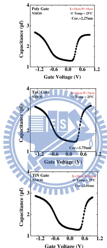
in Table 2.1 [2][3][21] and Fig. 2-2, actually induces the profoundest influence on threshold voltage. So, even though polysilicon gate device shows the lowest in Fig. 2-3 due to poly-depletion capacitance [22], still has the lowest threshold voltage among the three devices. Similar results for PMOS are shown in Fig. 2-4 and 2-5.
Before discussing roll-off, we need to know how the gate influences the formation of inversion layer under DT-mode. In subthreshold region, would lower the potential barrier height of the source node [23]:
(eq. 2-6)
is the intrinsic potential of source node. In the thermal equilibrium
( :
(eq. 2-7)
is the surface potential, and is the intrinsic potential of p- junction for p type substrate and type source region.
On other hand, the influences of body bias on surface potential is negligible due to no inversion charge, so can be consider as a function of only normal bias [20][23]. In addition, the lowing of induced by could promote the formation of inversion layer, so we define the gate control capability of DTMOS in subthreshold region as following:
(def. 2-3)
We know that applying to the substrate is equivalent to dropping the voltages of all other node of the device, namely, gate, drain, and source, by . So, now the
11
normal bias equals [23], and we have the following relationship:
(eq. 2-8)
Differentiating eq.2-8 with respect to yields:
(eq. 2-9)
is the capacitance of depletion layer. The relative change of and is calculated as:
(eq. 2-10)
On the other hand, the relative change of and is calculated as following: (eq. 2-11)
So, def. 2-3 is calculated as: (eq. 2-12)
According to eq. 2-7, while equals , a large amount of electrons inject to the surface from source node, and then inversion layer is formed. Now would influences not only but also due to the injection of inversion charge. Finally the surface potential begins to couple with the body bias.
12
From mathematics viewpoint, according to eq. 2-12, lower
and higher could increase the result value. Furthermore, we use body effect parameter as following to figure out the gate control capability:
(def. 2-4)
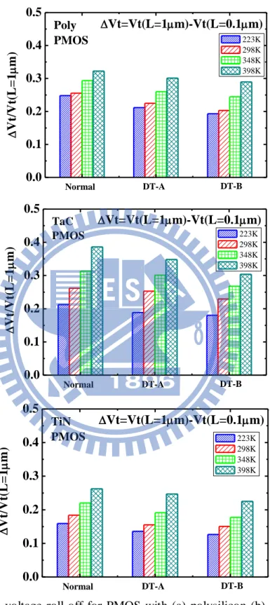
As shown in Fig. 2-6, metal gates would have better gate control capability, especially at low temperature, and thus improve the roll-off as in Fig. 2-7.
Ideally, if equals 1, no matters how
changes, the gate control capability would not be effected and always equals 1, but in reality, there are some non-ideal factors existing, such as substrate parasitic resistance [7], so the gate control capability under DT-B mode don’t equal 1, and it changes from device to device. For all this, the roll-off under DT-B mode is still improved much better than the other two modes as usual.
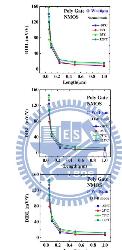
2.3.1.3 Characteristics of Drain Induced Barrier Lowing (DIBL)
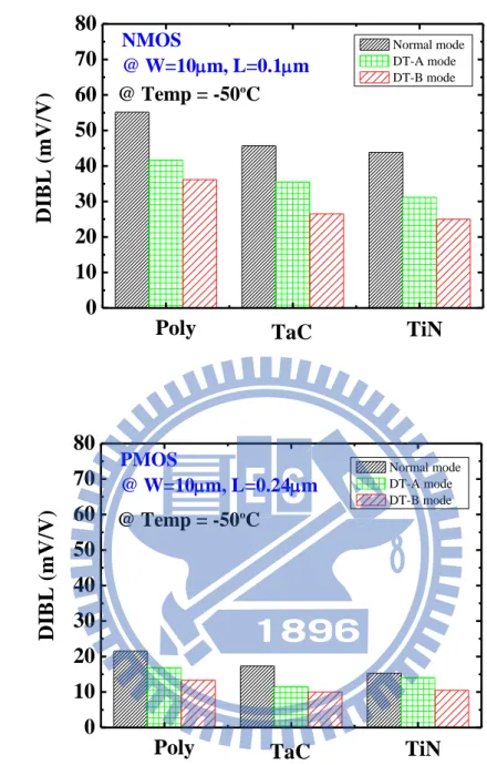
Source and drain depletion regions are a certain fraction of the channel. When the effective channel length is shorter, the drain is closer to the source, and can influence , so that the channel carrier concentration at that location is no longer fixed, and short channel effect (SCE) starts to occur. The lowing of causes an injection of extra carriers, thereby increasing the currents in both on-state and subthreshold regimes, so, short would enhance DIBL effect as shown in Fig. 2-8 and 2-9, and also result in higher subthreshold swing as shown in next section [20]. Under DT-mode, due to the narrower S/D depletion width induced by forward body bias, DT-B mode shows the lowest DIBL [7]. In addition, the two metal gates
13
exhibit their inherent stronger gate control capability once more as shown in Fig. 2-10.
Being worth mentioning, the DIBL effect is defined as the vertical parallel shift of curve at a given drain voltage and elevated drain voltage in the subthreshold regime [24]. For PMOS counterparts, long-channel behavior is totally lost while scaling down to 0.1 , and the curves are no longer vertical parallel; as a result, the gate length small than 0.1 is not discussed here.
2.3.1.4 Characteristics of Subthreshold Swing
When , the corresponding drain current is called the subthreshold current. In weak inversion and depletion, the electron charge is small and the drain current is dominated by diffusion. According to def. 2-3, we can deduce that subthreshold current for DTMOS could be as following [23]:
(eq. 2-13)
According to def. 2-2, subthreshold swing of DTMOS can now be calculated as:
(eq. 2-14)
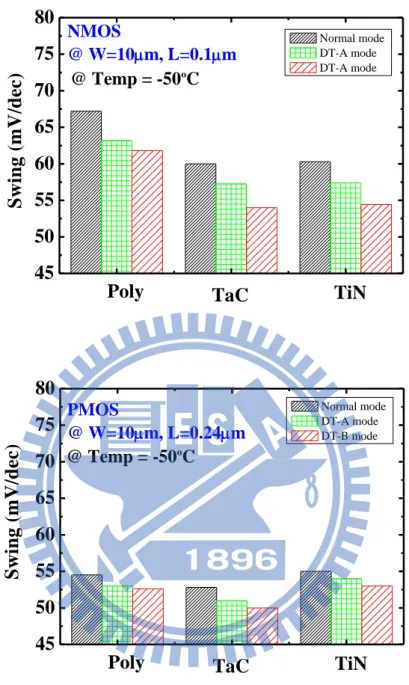
According to ex-part about DIBL, we’ve known that SCE would induce higher subthreshold swing as in Fig. 2-11 and 2-12. Furthermore, as in Fig. 2-13, metal gate devices under DT-B mode unfold the better performance again due to their excellent gate control capability.
As well as DIBL, while down to sub-0.1 the subthreshold swing for PMOS counterparts become too worst to be extracted; massive increasing of above-threshold and subthreshold currents cause those devices not turned off any more.
14
2.3.2 Comparison of Performance for DTMOS under Different Operation Temperatures
In the section, by comparing the experimental data with theoretical concepts, we present a study of the temperature dependence on the electric characteristics for DTMOS.
From the basic equations as shown as following [25]:
(eq. 2-15) and
(eq. 2-16) is the energy gap at T= 0K, we abtain:
(eq. 2-17) and
(eq. 2-18)
According to def. 2-4 and eq. 2-17, we know that:
(eq. 2-19)
In terms of eq. 2-18 and 2-19, elevated temperature results in threshold voltage reduction and degradation of gate control capability as shown in Fig. 2-6 [24][26-27]. Hence high temperature deteriorates SCE, such as roll-off, DIBL, and subthreshold swing shown as from Fig. 2.-14 to Fig. 2-37.
In addition, in order to derive the detailed temperature dependence of subthreshold
swing, we start from eq. 2-14 where the terms and
15
temperature while , so the subthershold swing of DTMOS would be more sensitive in temperature.
2.3.3 Existence of ZTC point for DTMOS
According Fig. 2-38, we infer that there is a way to obtain low leakage and high on-state current at the same time: If the ZTC point for DTMOS exists, we could apply higher than , the ZTC bias, under low temperature operation to obtain the excellent current gain.
From Fig. 2-39, regardless of normal or DT modes, a remarkable staggered spot appears, that’s a strong evidence of the existence of ZTC point. By far, the phenomenon is more obvious in Fig. 2-40. At , the drain current at high temperature is high due to ; at , since the ZTC point appears, the curves collaborate with each other; At , high temperature results in low on-state current, and then we can deduce that
. After proving the existence of ZTC point, now we are going to deliberate the theoretical model of ZTC point for DTMOS in next chapter to help us achieve the excellent current gain.
2.4 Summary
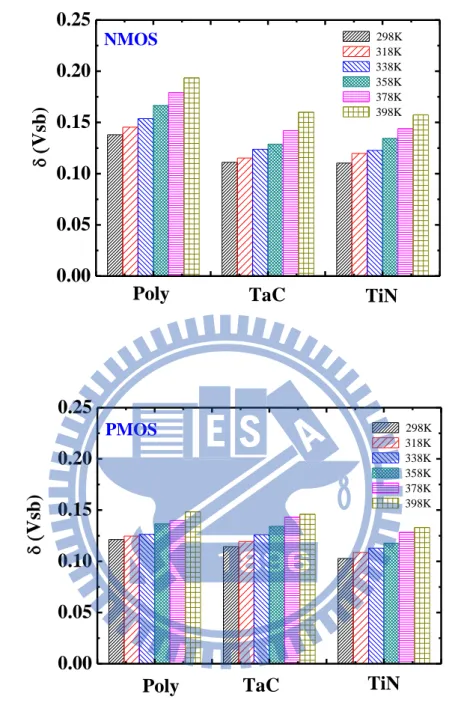
In the session, we define the gate control capability for DTMOS. From the theoretical inference process, we find that higher and lower can result in higher gate control capability; on the other hand, from the experimental results, metal gates have lower than polysilicon gate, and low temperature operation further reduces , so metal gate devices under DT-B mode at low temperature operation bring about best gate control capability, along with excellent performance, such as
16
improved roll-off, better DIBL, and lower subthreshold swing.
In the end of the chapter, we show the existence of ZTC point for DTMOS, which could tell us how to hypothesize the supply voltage to get the best current gain under low temperature operation.
17 (a)
(b)
(C)
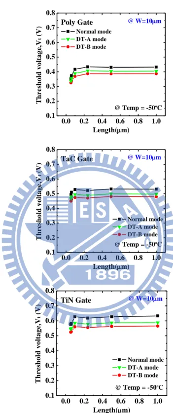
Fig. 2-1 Drain current versus gate voltage for NMOS with (a) polysilicon (b) TaC (c) TiN gate under normal, DT-A and DT-B modes. The operation temperature is fixed at 223K. 0.0 0.2 0.4 0.6 0.8 1.0 10-13 10-11 10-9 10-7 10-5 10-3 10-1 101 @ Temp = -50o C Poly Gate NMOS L=0.055m,W=10m D r a in c u r r e n t (A ) Gate voltage (V) Normal mode Vd=0.7 DT-A mode Vd=0.7 DT-B mode Vd=0.7 0.0 0.2 0.4 0.6 0.8 1.0 10-13 10-11 10-9 10-7 10-5 10-3 10-1 101 @ Temp = -50o C TiN Gate NMOS L=0.055m,W=10m D r a in c u r r e n t (A ) Gate voltage (V) Normal mode Vd=0.7 DT-A mode Vd=0.7 DT-B mode Vd=0.7 0.0 0.2 0.4 0.6 0.8 1.0 10-13 10-11 10-9 10-7 10-5 10-3 10-1 101 @ Temp = -50oC TaC Gate NMOS L=0.055m,W=10m D r a in c u r r e n t (A ) Gate voltage (V) Normal mode Vd=0.7 DT-A mode Vd=0.7 DT-B mode Vd=0.7
18
Table 2.1 Effective work function lists.
Poly-Si TaC TiN
NMOS_EWF (eV) 4.1 4.45 4.7
19 (a)
(b)
(C)
Fig. 2-2 Threshold voltage versus gate length for NMOS with (a) polysilicon (b) TaC (c) TiN gate under normal, DT-A and DT-B modes. The operation temperature is fixed at 223K. 0.0 0.2 0.4 0.6 0.8 1.0 0.1 0.2 0.3 0.4 0.5 0.6 0.7 0.8 Normal mode DT-A mode DT-B mode @ W=10m T h r e sh o ld v o lt a g e ,V t ( V ) Length(m) @ Temp = -50oC TiN Gate 0.0 0.2 0.4 0.6 0.8 1.0 0.1 0.2 0.3 0.4 0.5 0.6 0.7 0.8 Normal mode DT-A mode DT-B mode @ W=10m T h r e sh o ld v o lt a g e ,V t ( V ) Length(m) @ Temp = -50oC TaC Gate 0.0 0.2 0.4 0.6 0.8 1.0 0.1 0.2 0.3 0.4 0.5 0.6 0.7 0.8 Normal mode DT-A mode DT-B mode @ W=10m T h r e sh o ld v o lt a g e ,V t ( V ) Length(m) @ Temp = -50o C Poly Gate
20 (a)
(b)
(C)
Fig. 2-3 High frequency C-V characteristics at 1 MHz for NMOS with (a) polysilicon (b) TaC (c) TiN gate.
-1.2 -0.6 0.0 0.6 1.2 1 2 3 4 Cor.=2.01nm L=10m,W=10m @ Temp = 25oC TiN Gate NMOS C a p a c it a n c e ( p f) Gate Voltage (V) -1.2 -0.6 0.0 0.6 1.2 1 2 3 4 L=10m,W=10m @ Temp = 25o C Poly Gate NMOS C a p a c it a n c e ( p f) Gate Voltage (V) Cor.=2.27nm -1.2 -0.6 0.0 0.6 1.2 1 2 3 4 Cor.=1.75nm L=10m,W=10m @ Temp = 25oC TaC Gate NMOS C a p a c it a n c e ( p f) Gate Voltage (V)
21 (a)
(b)
(C)
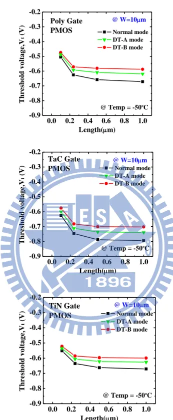
Fig. 2-4 Threshold voltage versus gate length for PMOS with (a) polysilicon (b) TaC (c) TiN gate under normal, DT-A and DT-B modes. The operation temperature is fixed at 223 K. 0.0 0.2 0.4 0.6 0.8 1.0 -0.9 -0.8 -0.7 -0.6 -0.5 -0.4 -0.3 -0.2 Normal mode DT-A mode DT-B mode @ W=10m T h r e sh o ld v o lt a g e ,V t ( V ) Length(m) @ Temp = -50oC Poly Gate PMOS 0.0 0.2 0.4 0.6 0.8 1.0 -0.9 -0.8 -0.7 -0.6 -0.5 -0.4 -0.3 -0.2 Normal mode DT-A mode DT-B mode @ W=10m T h r e sh o ld v o lt a g e ,V t ( V ) Length(m) @ Temp = -50oC TaC Gate PMOS 0.0 0.2 0.4 0.6 0.8 1.0 -0.9 -0.8 -0.7 -0.6 -0.5 -0.4 -0.3 -0.2 Normal mode DT-A mode DT-B mode @ W=10m T h r e sh o ld v o lt a g e ,V t ( V ) Length(m) @ Temp = -50oC TiN Gate PMOS
22 (a) (b) (C)
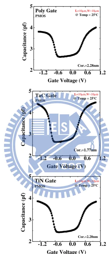
Fig. 2-5 High frequency C-V characteristics at 1 MHz for PMOS with (a) polysilicon (b) TaC (c) TiN gate.
-1.2 -0.6 0.0 0.6 1.2 2 3 4 5 L=10m,W=10m @ Temp = 25oC TiN Gate PMOS C a p a c it a n c e ( p f) Gate Voltage (V) Cor.=2.28nm -1.2 -0.6 0.0 0.6 1.2 2 3 4 5 Cor.=2.28nm L=10m,W=10m @ Temp = 25oC Poly Gate PMOS C a p a c it a n c e ( p f) Gate Voltage (V) -1.2 -0.6 0.0 0.6 1.2 2 3 4 5 Cor.=1.77nm L=10m,W=10m @ Temp = 25oC TaC Gate PMOS C a p a c it a n c e ( p f) Gate Voltage (V)
23 (a)
(b)
Fig. 2-6 of polysilicon, TaC, and TiN gates over a range of operation temperature from 298K to 398K for (a) NMOS (b) PMOS.
0.00 0.05 0.10 0.15 0.20 0.25 NMOS TiN TaC Poly V sb ) 298K 318K 338K 358K 378K 398K 0.00 0.05 0.10 0.15 0.20 0.25 V sb ) PMOS TiN TaC Poly 298K 318K 338K 358K 378K 398K
24 (a)
(b)
Fig. 2-7 Threshold voltage roll-off characteristics of (a) NMOS (b) PMOS with polysilicon, TaC and TiN gate under normal, DT-A and DT-B modes, respectively. The operation temperature is fixed at 223K.
0.00 0.05 0.10 0.15 0.20 0.25 0.30 Vt=Vt(L=1m)-Vt(L=0.055m) Vt /Vt (L = 1 m ) @ Temp = -50NMOS@ W=10oCm Normal mode DT-A mode DT-B mode
Poly TaC TiN
0.00 0.05 0.10 0.15 0.20 0.25 0.30 Vt=Vt(L=1m)-Vt(L=0.1m) Vt /Vt (L = 1 m ) PMOS@ W=10m@ Temp = -50o C Normal mode DT-A mode DT-B mode
25 (a)
(b)
(C)
Fig. 2-8 DIBL versus gate length for NMOS with (a) polysilicon (b) TaC (c) TiN gate under normal, DT-A and DT-B modes. The operation temperature is fixed at 223K.
0.0 0.2 0.4 0.6 0.8 1.0 0 50 100 150 200 Normal mode DT-A mode DT-B mode @ W=10m D IB L ( m V /V ) Length(m) @ Temp = -50oC Poly Gate NMOS 0.0 0.2 0.4 0.6 0.8 1.0 0 50 100 150 200 Normal mode DT-A mode DT-B mode @ W=10m D IB L ( m V /V ) Length(m) @ Temp = -50oC TaC Gate NMOS 0.0 0.2 0.4 0.6 0.8 1.0 0 50 100 150 200 Normal mode DT-A mode DT-B mode @ W=10m D IB L ( m V /V ) Length(m) @ Temp = -50oC TiN Gate NMOS
26 (a)
(b)
(C)
Fig. 2-9 DIBL versus gate length for PMOS with (a) polysilicon (b) TaC (c) TiN gate under normal, DT-A and DT-B modes. The operation temperature is fixed at 223K.
0.0 0.2 0.4 0.6 0.8 1.0 0 50 100 150 200 Normal mode DT-A mode DT-B mode @ W=10m D IB L ( m V /V ) Length(m) @ Temp = -50oC Poly Gate PMOS 0.0 0.2 0.4 0.6 0.8 1.0 0 50 100 150 200 Normal mode DT-A mode DT-B mode @ W=10m D IB L ( m V /V ) Length(m) @ Temp = -50o C TaC Gate PMOS 0.0 0.2 0.4 0.6 0.8 1.0 0 50 100 150 200 Normal mode DT-A mode DT-B mode @ W=10m D IB L ( m V /V ) Length(m) @ Temp = -50oC TiN Gate PMOS
27 (a)
(b)
Fig. 2-10 DIBL of (a) NMOS (b) PMOS with polysilicon, TaC and TiN gate under normal, DT-A and DT-B modes, respectively. The operation temperature is fixed at 223K. 0 10 20 30 40 50 60 70 80 D IB L ( m V /V ) NMOS @ W=10m, L=0.1m @ Temp = -50o C Normal mode DT-A mode DT-B mode
Poly TaC TiN
0 10 20 30 40 50 60 70 80 D IB L ( m V /V ) PMOS @ W=10m, L=0.24m @ Temp = -50oC Normal mode DT-A mode DT-B mode
28 (a)
(b)
(C)
Fig. 2-11 Subthershold swing versus gate length for NMOS with (a) polysilicon (b) TaC (c) TiN gate under normal, DT-A and DT-B modes. The operation temperature is fixed at 223K. 0.0 0.2 0.4 0.6 0.8 1.0 40 60 80 100 @ Temp = -50oC Poly Gate NMOS @ W=10m Normal mode DT-A mode DT-B mode S w in g ( m V /d e c ) Lengthth(m) 0.0 0.2 0.4 0.6 0.8 1.0 40 60 80 100 @ Temp = -50o C TaC Gate NMOS @ W=10m Normal mode DT-A mode DT-B mode S w in g ( m V /d e c ) Lengthth(m) 0.0 0.2 0.4 0.6 0.8 1.0 40 60 80 100 @ Temp = -50oC TiN Gate NMOS @ W=10m Normal mode DT-A mode DT-B mode S w in g ( m V /d e c ) Lengthth(m)
29 (a)
(b)
(C)
Fig. 2-12 Subthershold swing versus gate length for PMOS with (a) polysilicon (b) TaC (c) TiN gate under normal, DT-A and DT-B modes. The operation temperature is fixed at 223K. 0.0 0.2 0.4 0.6 0.8 1.0 40 60 80 100 @ Temp = -50o C Poly Gate PMOS @ W=10m Normal mode DT-A mode DT-B mode S w in g ( m V /d e c ) Lengthth(m) 0.0 0.2 0.4 0.6 0.8 1.0 40 60 80 100 @ Temp = -50oC TaC Gate PMOS @ W=10m Normal mode DT-A mode DT-B mode S w in g ( m V /d e c ) Lengthth(m) 0.0 0.2 0.4 0.6 0.8 1.0 40 60 80 100 @ Temp = -50oC TiN Gate PMOS @ W=10m Normal mode DT-A mode DT-B mode S w in g ( m V /d e c ) Lengthth(m)
30 (a)
(b)
Fig. 2-13 Subthershold swing of (a) NMOS (b) PMOS with polysilicon, TaC and TiN gate under normal, DT-A and DT-B modes, respectively. The operation temperature is fixed at 223K. 45 50 55 60 65 70 75 80 S w in g ( m V /d e c ) NMOS @ W=10m, L=0.1m @ Temp = -50oC Normal mode DT-A mode DT-A mode
Poly TaC TiN
45 50 55 60 65 70 75 80 S w in g ( m V /d e c ) PMOS @ W=10m, L=0.24m @ Temp = -50oC Normal mode DT-A mode DT-B mode
31 (a)
(b)
(C)
Fig. 2-14 Threshold voltage versus gate length for NMOS with polisilicon gate under (a) normal (b) DT-A (c) DT-B gate mode for different temperatures. The operation temperatures are fixed at 223K, 298K, 348K, and 398K, respectively.
0.0 0.2 0.4 0.6 0.8 1.0 0.1 0.2 0.3 0.4 0.5 0.6 0.7 0.8 -50o C 25o C 75o C 125o C @ W=10m T h r e sh o ld v o lt a g e ,V t ( V ) Length(m) Poly Gate
NMOS Notmal mode
0.0 0.2 0.4 0.6 0.8 1.0 0.1 0.2 0.3 0.4 0.5 0.6 0.7 0.8 -50o C 25o C 75o C 125o C @ W=10m T h r e sh o ld v o lt a g e ,V t ( V ) Length(m) Poly Gate
NMOS DT-A mode
0.0 0.2 0.4 0.6 0.8 1.0 0.1 0.2 0.3 0.4 0.5 0.6 0.7 0.8 -50o C 25o C 75o C 125o C @ W=10m T h r e sh o ld v o lt a g e ,V t ( V ) Length(m) Poly Gate NMOS DT-B mode
32 (a)
(b)
(C)
Fig. 2-15 Threshold voltage versus gate length for NMOS with TaC gate under (a) normal (b) DT-A (c) DT-B gate mode for different temperatures. The operation temperatures are fixed at 223K, 298K, 348K, and 398K, respectively.
0.0 0.2 0.4 0.6 0.8 1.0 0.1 0.2 0.3 0.4 0.5 0.6 0.7 0.8 -50o C 25o C 75o C 125o C @ W=10m T h r e sh o ld v o lt a g e ,V t ( V ) Length(m) TaC Gate
NMOS Normal mode
0.0 0.2 0.4 0.6 0.8 1.0 0.1 0.2 0.3 0.4 0.5 0.6 0.7 0.8 -50o C 25o C 75o C 125o C @ W=10m T h r e sh o ld v o lt a g e ,V t ( V ) Length(m) TaC Gate
NMOS DT-A mode
0.0 0.2 0.4 0.6 0.8 1.0 0.1 0.2 0.3 0.4 0.5 0.6 0.7 0.8 -50o C 25o C 75o C 125o C @ W=10m T h r e sh o ld v o lt a g e ,V t ( V ) Length(m) TaC Gate NMOS DT-B mode
33 (a)
(b)
(C)
Fig. 2-16 Threshold voltage versus gate length for NMOS with TiN gate under (a) normal (b) DT-A (c) DT-B gate mode for different temperatures. The operation temperatures are fixed at 223K, 298K, 348K, and 398K, respectively.
0.0 0.2 0.4 0.6 0.8 1.0 0.1 0.2 0.3 0.4 0.5 0.6 0.7 0.8 -50o C 25o C 75o C 125o C @ W=10m T h r e sh o ld v o lt a g e ,V t ( V ) Length(m) TiN Gate
NMOS Normal mode
0.0 0.2 0.4 0.6 0.8 1.0 0.1 0.2 0.3 0.4 0.5 0.6 0.7 0.8 -50o C 25o C 75o C 125o C @ W=10m T h r e sh o ld v o lt a g e ,V t ( V ) Length(m) TiN Gate
NMOS DT-A mode
0.0 0.2 0.4 0.6 0.8 1.0 0.1 0.2 0.3 0.4 0.5 0.6 0.7 0.8 -50o C 25oC 75o C 125o C @ W=10m T h r e sh o ld v o lt a g e ,V t ( V ) Length(m) TiN Gate NMOS DT-B mode
34 (a)
(b)
(C)
Fig. 2-17 Threshold voltage roll-off for NMOS with (a) polysilicon (b) TaC (c) TiN gate under normal, DT-A, DT-B gate mode for different operation temperatures. The operation temperatures are fixed at 223K, 298K, 348K, and 398K, respectively.
0.00 0.05 0.10 0.15 0.20 Vt /Vt (L = 1 m ) Vt=Vt(L=1m)-Vt(L=0.06m) DT-B DT-A 223K 298K 348K 398K Normal Poly NMOS 0.00 0.05 0.10 0.15 0.20 Vt=Vt(L=1m)-Vt(L=0.06m) Vt /Vt (L = 1 m ) DT-B DT-A 223K 298K 348K 398K Normal TaC NMOS 0.00 0.05 0.10 0.15 0.20 Vt /Vt (L = 1 m ) Vt=Vt(L=1m)-Vt(L=0.06m) DT-B DT-A 223K 298K 348K 398K Normal TiN NMOS
35 (a)
(b)
(C)
Fig. 2-18 Threshold voltage versus gate length for PMOS with polisilicon gate under (a) normal (b) DT-A (c) DT-B gate mode for different temperatures. The operation temperatures are fixed at 223K, 298K, 348K, and 398K, respectively.
0.0 0.2 0.4 0.6 0.8 1.0 -0.9 -0.8 -0.7 -0.6 -0.5 -0.4 -0.3 -0.2 -50o C 25oC 75o C 125o C @ W=10m T h r e sh o ld v o lt a g e ,V t ( V ) Length(m) Poly Gate
PMOS Notmal mode
0.0 0.2 0.4 0.6 0.8 1.0 -0.9 -0.8 -0.7 -0.6 -0.5 -0.4 -0.3 -0.2 -50o C 25o C 75o C 125o C @ W=10m T h r e sh o ld v o lt a g e ,V t ( V ) Length(m) Poly Gate PMOS DT-A mode 0.0 0.2 0.4 0.6 0.8 1.0 -0.9 -0.8 -0.7 -0.6 -0.5 -0.4 -0.3 -0.2 -50o C 25o C 75o C 125o C @ W=10m T h r e sh o ld v o lt a g e ,V t ( V ) Length(m) Poly Gate PMOS DT-B mode