國 立 交 通 大 學
電信工程學系
碩士論文
寬頻微波耦合器與濾波器
Broadband Microwave Coupler and Filter
研究生:陳永順
指導教授:張志揚 博士
寬頻微波耦合器與濾波器
Broadband Microwave Coupler and Filter
研 究 生:陳永順 Student:Yong-Shun Chen
指導教授:張志揚 博士 Advisor:Dr. Chi-Yang Chang
國立交通大學
電信工程學系
碩士論文
A Thesis
Submitted to Department of Communication Engineering
College of Electrical and Computer Engineering
National Chiao Tung University
in Partial Fulfillment of the Requirements
for the Degree of
Master of Science
in
Communication Engineering
June 2006
Hsinchu, Taiwan, Republic of China
寬頻微波耦合器與濾波器
研究生:陳永順
指導教授:張志揚博士
國立交通大學電信工程學系
摘 要
本篇論文包含兩類微波電路分別是小型化的超寬頻 90
03dB的耦合器和
多層寬頻帶通濾波器。
首先採用 5 節對稱式串接的共平面波導架構來實現超寬頻(2-18GHz)
90
03dB的耦合器,並利用垂直安裝平面(VIP)基板來達到中心節強耦合的需
求,還補償了中心節奇偶模相位速度不相等的問題,最後實作電路採用高
電介質的母基板(
εr =9.8)來達到小型化的電路尺寸(16 .8mm×6 mm
)。寬頻(2-4GHz)帶通濾波器則是利用平行耦合的步階阻抗諧振器來達
成,步階阻抗諧振器(SIR)有兩個優點,分別是有效減小諧振器的長度達到
縮小化和抑制上止帶高階模的干擾,最後利用多層結構來達到強耦合並實
現中心頻 3GHz、比例頻寬 66.67%和高止帶抑制的帶通濾波器。
Broadband Microwave Coupler and Filter
Student: Yong-Shun Chen Advisor: Dr. Chi-Yang Chang
Department of Communication Engineering
National Chiao Tung University
Abstract
The thesis includes the two kinds of microwave circuits, namely the miniaturized ultra-broadband quadrature hybrid coupler and the multilayer wideband bandpass filter.
We adopt a 5-section symmetrical cascaded coplanar waveguide (CPW) structure to
realize the ultra-broadband (2-18GHz) quadrature hybrid coupler. In the tightest center coupling section, we propose the vertically installed planar (VIP) structure to achieve it
and also compensate the unequal odd- and even-mode phase velocities. The fabricated circuit
size miniaturized by high dielectric substrate (εr =9.8) is 16.8 mm×6 mm.
Then, a wideband (2-4GHz) bandpass filter is designed by using parallel coupled line stepped impedance resonators (SIR). The properties of SIR can reduce the resonant length and suppress the upper stopband interference. Furthermore, we propose multilayer structure to obtain the tight-coupling. Finally, a wideband filter with center frequency at 3 GHz, 66.67% fractional bandwidth, and high stopband rejection is presented.
Acknowledgement
致謝
本篇論文得以順利完成,首要感謝指導教授張志揚博士,在研究上的指
導與鼓勵,讓我在微波電路上獲益良多。同時要感謝口試委員郭仁財教授、
邱煥凱教授和林育德教授的不吝指教使論文更加完善。
感謝陳慧諄學長在模擬軟體與電路實作技巧上的教導,使我能很快的上
手。謝謝實驗室同學佩綾、郭巴、哲慶、中宏,伴我度過兩年氣氛融洽的
實驗室生活,並在學業和生活上給予協助或幫忙。
最後,要特別感謝我的父母親,在求學生涯對我的鼓勵與生活上的支
持,謝謝你們。
NCTU LAB916 2006.06.23Content
Abstract (Chinese)……….………..………i Abstract………...…………..………..………ii Acknowledgment………..……….iii Content……….……….………...iv List of Tables………...………..………..……….. vi List of Figures…………...……….…………...………..vii Chapter 1 Introduction…….……...……….…………...………...1Chapter 2 Miniaturized Ultra-Broadband (2-18GHz) Quadrature Hybrid Coupler……...2
2.1 Introduction... …...………2
2.2 Theory……….... …………..……….………..4
2.2-1 The theory of the coupler – odd- and even-mode excitations.. .... ……..………6
2.2-2 The analysis of the conventional CPW coupler ………….…….... ….…….…10
2.2-3 The analysis of the loose-coupling CPW coupler……….………….12
2.2-4 The analysis of the vertically installed planar (VIP) coupler.…...………13
2.3 Design procedure and Simulation…..………...………….……15
2.3-1 The loose-coupling section (section 1 and section 5)…….….………..…15
2.3-2 The middle-coupling section (section 2 and section 4) …...……….18
2.3-3 The tight-coupling section (center section) ………...………...20
2.3-4 The total cascaded circuit………...………...23
2.4 Circuit fabrication and Measurement……….………...…..………….…..26
Chapter 3 Multilayer Wideband Bandpass Filter……….…………...…….………...…...30
3.1 Introduction………...………....……….…………...…..………...30
3.3 Design procedure and Simulation……..……….…...………36
3.4 Circuit fabrication and Measurement…...….…...……...…….………..43
Chapter 4 Conclusion………..………….………..45
List of Tables
Table 2.1 Parameters of a five-section, symmetrical and ultra-broadband (2-18GHz)
quadrature hybrid coupler………..………….…………..………. 5 Table 3.1 The geometrical dimensions of the wideband bandpass filter….………….………42
List of Figures
Fig. 2.1 (a) A five-section symmetrical and (b) asymmetrical couplers………...……...……5
Fig. 2.2 Top view of the CPW coupler structure………...6
Fig. 2.3 The equivalent circuit of coupler……….………...6
Fig. 2.4 (a) The odd-mode equivalent circuit of coupler..………....….….….6
Fig. 2.4 (b) The even-mode equivalent circuit of coupler……..………...7
Fig. 2.5 The simplified (a) odd- and (b) even equivalent circuits of couplers….... ……....…7
Fig. 2.6 (a) Top and (b) cross-sectional views of the CPW coupled line…………...…..10
Fig. 2.7 (a) Even- and (b) odd-mode equivalent circuits of the CPW coupled line. …….…10
Fig. 2.8 The CPW coupler structure after inserting the ground strip between two coupled lines……..………..………...………...…..…..12
Fig. 2.9
(a)Even- and (b) odd-mode equivalent circuits of the CPW coupled line after inserting the ground strip between two coupled lines………...………..12
Fig. 2.10 (a) Cross-sectional view and (b) full view of the VIP structure………....….13
Fig. 2.11 (a) Even- and (b) odd-mode equivalent circuits of the VIP structure….…...14
Fig. 2.12 The compensated VIP structure with dielectric blocks (εr =3.38)…….………..15
Fig. 2.13 The cross-sectional view of the loose-coupling section……….…...16
Fig. 2.14 (a) Even- mode excitation..………...……….…….16
Fig. 2.14 (b) Odd-mode excitation..………...………...…….……17
Fig. 2.15 (a) The simulated results of the loose-coupling section………...……..……17
Fig. 2.15 (b) Even- and odd-mode phases of the loose-coupling section….………...……..17
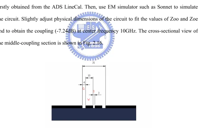
Fig. 2.16 The cross-sectional view of the middle-coupling section………..……….………18
Fig. 2.17 (b) Even- and odd-mode phases of the middle-coupling section.………….….…19
Fig. 2.18 3D diagram of the VIP structure in HFSS……….………….………20
Fig. 2.19 (a) The simulated results of the tight-coupling section……….……….21
Fig. 2.19 (b) Even- and odd-mode phases of the tight-coupling section………….…..……21
Fig. 2.20 The compensated VIP structure……….……….…22
Fig. 2.21 (a) The simulated results of the compensated tight-coupling section……...22
Fig. 2.21 (b) Even- and odd-mode phases of the compensated tight-coupling sectio……...22
Fig. 2.22 The total cascaded circuit in Microwave Office……….…………23
Fig. 2.23 The simulated results by Microwave Office……….………..…23
Fig. 2.24 The total modified cascaded circuit in Microwave Office…….…………...24
Fig. 2.25 The modified simulated results by Microwave Office……….………24
Fig. 2.26 The total circuit in HFSS……….………...25
Fig. 2.27 (a) The simulated results of the total circuit by HFSS………....25
Fig. 2.27 (b) Phases of the coupled and through port………...25
Fig. 2.28 Photos of (a) the fabricated 5-section hybrid coupler and (b) the fabricated 5-section hybrid coupler with dielectrics………..…………..26
Fig. 2.29 (a) The measured results of the total circuit without dielectrics.………26
Fig. 2.29 (b) Phases of the coupled and through port……….………...27
Fig. 2.29 (c) The amplitude and phase errors between the coupled and through port……...27
Fig. 2.30 (a) The measured results of the total circuit with dielectric blocks.…..…...28
Fig. 2.30 (b) Phases of the coupled and through port……….………...28
Fig. 2.31 The measured and simulated amplitude and phase errors between the coupled and through port………….…..……….……28
Fig. 3.1 Structures of the SIR (a) K = Z2/Z1 < 1 (b) K = Z2/Z1 > 1……….….………..31
Fig. 3.2 (a) Parallel coupled line and (b) its equivalent circuit.………..………...33
Fig. 3.4 The wideband bandpass filter model………….………..….36
Fig. 3.5 The wideband bandpass filter response……….………..…..…...37
Fig. 3.6 3-layer structure……….………..….……38
Fig. 3.7 (a) Odd-mode and (b) even-mode equivalent circuits………..….…...38
Fig. 3.8 The 3D diagram of even- and odd-mode excitations in HFSS…………. ….……..39
Fig. 3.9 (a) Even-mode characteristic impedances versus G and W………..……....39
Fig. 3.9 (b) Even-mode effective dielectric constants versus G and W………….……...39
Fig. 3.9 (c) Odd-mode characteristic impedances versus G and W………..…….40
Fig. 3.9 (d) Odd-mode effective dielectric constants versus G and W………..…...40
Fig. 3.9 (e) Characteristic impedances and effective dielectric constants of the high impedance line versus G………..…………...……41
Fig. 3.10 (a) 3D view of the wideband bandpass filter diagram………... …...…..41
Fig. 3.10 (b) Cross-sectional view of the wideband bandpass filter diagram…………...….42
Fig. 3.11 Simulated results of the wideband band filter…...………....….….42
Fig. 3.12 (a) Front-side and (b) back-side views of the circuit photos………... …....…..…43
Chapter 1
Introduction
In microwave broadband communication systems, high performance broadband directional coupler and bandpass filter are two key components. This thesis, therefore, is focused on these components. Miniaturization and low-cost will also be main issues.
In chapter 2, we apply the high dielectric constant substrate (εr =9.8) to miniaturize the
circuit size and utilize the VIP structure to overcome the tight-coupling problem. The VIP coupled-line structure can supply a high even-mode characteristic impedance and a low odd-mode characteristic impedance in the same time. As a result, a very tight coupling can be implemented. Furthermore, we also propose a method to compensate the unequal even- and odd-mode phase velocities by putting dielectric blocks at both sides of the VIP substrate. The directivity of the VIP coupler improves drastically. Finally, a miniaturized 5-section CPW ultra-broadband quadrature hybrid coupler is realized.
In chapter 3, we adopt parallel coupled stepped impedance resonators (SIR) to realize a wideband bandpass filter. The SIR can not only reduce the resonant length but also make the first spurious resonant frequency much higher than twice of the passband center frequency. The effect can be enhanced by adjusting the impedance ratio of the high-Z and low-Z segments. Due to this advantage, the spurious passband response can be pushed to a very high frequency. Moreover, we propose a multilayer structure to satisfy the required filter parameters. The proposed multilayer structure can provide the extremely tight-coupling as well as a high to low even-mode characteristic impedances. Finally, we utilize the proposed structures to implement a wideband bandpass filter.
In chapter 4, we compare the measured results with the simulated results and make a conclusion for the designed circuits.
Chapter 2
Miniaturized Ultra-Broadband (2-18GHz)
Quadrature Hybrid Coupler
2.1 Introduction
Ultra-broadband (2-18GHz) quadrature hybrid coupler is one of the most important devices in the ultra-broadband antenna mode former network. To obtain an approximately constant coupling over a wider frequency bandwidth, cascading a number of coupled sections is more feasible than using a single-section coupler. Each section is quarter wavelength at the center frequency. By properly choosing the odd- and even-mode characteristic impedances of the various sections, the bandwidth of the coupler increases accordingly. The theory of a multi-section quadrature hybrid [1][2] had been investigated completely and the design is tabled into the odd- and even-mode characteristic impedances of each section. According to the studies, a five-section TEM mode cascaded coupler is required to achieve the specifications of the ultra-broadband quadrature hybrid. Based on the analysis [1][2], however, we need to achieve the TEM mode restriction and the tightest center coupling section (-0.77dB). This is the most challenging work of this hybrid.
Although the papers [3][4] mentioned that using the multi-section nonuniform cascaded coupler in inhomogeneous media can achieve the ultra-broadband performance, the length of total circuit is much longer than the method in [1][2]. Besides, the complicated analysis, difficulty in layout, and extremely tight coupling at the center portion of the coupler limit the practical implementation.
Conventional approach to develop an ultra-broadband quadrature hybrid coupler is using stripline structure. The stripline structure has the advantages of equal even- and odd-mode
effective dielectric constants and TEM transmission mode. That is the same with the assumption of the theoretical analysis described in [1][2]. The broadside-coupled structure implements the tight coupling section (tighter than -3dB of coupling) in multi-section cascaded coupler. Nevertheless, stripline needs the complicated and accurate mechanical housing, otherwise the performance of the broadband coupler degrades. Most of striplines use
a low dielectric substrate (aboutεr=2.2) to reduce the sensitivity of the housing dimensions.
As a result, the circuit size is relatively large.
To solve the mentioned problems, we propose a coplanar waveguide (CPW) structure to realize an ultra-broadband quadrature hybrid coupler. The CPW can not only use high
dielectric constant (εr=9.8) substrate to shrink the circuit size but also be easy to fabricate
without complicated mechanical housing. Although microstrip lines have these two advantages, the junction’s discontinuity effects of microstrip lines at high frequency are not easy to control in a multi-section cascaded coupler. The CPW allows different geometrical dimensions [5] to minimize the discontinuity effect between coupling sections.
For the tight-coupling problem, several methods have been proposed in the literatures. One solution is to utilize tandem couplers to realize a tight-coupling coupler [6]. Using tandem coupler, the tightly coupled central section of a multi-section coupler might be achieved. Although this method can avoid the tight-coupling problem and is easy to implement, the tandem coupler consumes larger circuit area and has much stronger junction discontinuity effect. Another approach is to use interdigital layout to achieve the tight coupling [7][8]. However, it is still difficult to implement a coupler tighter than -3dB. Re-entrant structures [9]-[11] can achieve the tight coupling, but is not easy to fabricate by conventional PCB processes. We propose the vertically installed planar (VIP) structure [12] to satisfy the tight coupling. The VIP structure comprises a main horizontal substrate and a vertical (VIP) substrate. The structure does not need a complicated fabrication processes and takes the advantage of the broadside-coupled method to realize the tight coupling. The VIP
structure will be discussed further in Section 2.2-4.
The odd- and even-mode phase velocities of the quasi-TEM mode CPW structure are unequal. This characteristic often makes the performance of the broadband cascaded couplers worse. A compensating approach proposed in [13] that a dielectric layer is added on top of the coupled lines to equalize the odd- and even-mode phase velocities. We can take advantage of this method to overcome the challenge.
2.2 Theory
According to [1][2], the ultra-broadband (2-18GHz) quadrature hybrid coupler needs at least five-section TEM mode couplers as shown in Fig. 2.1 (a). The phase relationship between coupled and through port of the end-to-end symmetrical coupler is independent of the frequency. Due to this property, we adopt the symmetrical multi-section coupler. Asymmetrical multi-section couplers shown in Fig. 2.1 (b) do not exhibit the required
quadrature phase property. From [1], we find that a five-section, ± 0.5dB ripple level, and
frequency bandwidth ration B=9.62 can achieve the desired specifications. Then, we determine even-mode characteristic impedances of the various sections from the table in [1]. Once the even-mode characteristic impedances are known, we can find the odd-mode characteristic impedances and also the coupling in dB of various sections of the coupler as given in Table 2.1. From Table 2.1, we know that the 5-section coupler consists of the three kinds of coupled-lines, namely, loose, middle and tight couplings. In the following section we will describe the analysis method.
through
S1 S2 S3 S4 S5
input
coupled
isolated
Zoe1 Zoe2 Zoe3 Zoe4 Zoe5
Zoo1 Zoo2 Zoo3 Zoo4 Zoo5
Fig. 2.1 (a) A five-section symmetrical coupler
coupled
input
through
isolated
S1 S2 S3 S4 S5
Zoe1 Zoe2 Zoe3 Zoe4 Zoe5
Zoo1 Zoo2 Zoo3 Zoo4 Zoo5
Fig. 2.1 (b) A five-section asymmetrical coupler
S1&S5 S2&S4 S3 Zoe(Ω) 59.411 79.63 237.13 Zoo(Ω) 42.08 31.40 10.54 Coupling(dB) -15.35 -7.24 -0.77 δ (dB) 0.5 w 1.62357 B 9.62609
δ (passband ripple level)、w (fractional bandwidth)、 B (bandwidth ratio) Table 2.1 Parameters of a five-section, symmetrical and ultra-broadband (2-18GHz)
2.2-1 The theory of the coupler – odd- and even-mode excitations
We utilize the odd- and even-mode excitation to analyze the CPW coupler. The CPW coupler structure is shown in Fig. 2.2. The equivalent circuit of coupler is shown in Fig. 2.3 and the odd- and even-mode equivalent circuits are shown in Fig. 2.4(a) and (b), respectively.
Top View
Ground Ground
Coupled lines
Fig. 2.2 Top view of the CPW coupler structure
` ` ` ` o e
θ
θ
,
P o eZ
Z
0,
0 1 2 3 4 2V Z0 Z0 Z0 Z0 + _ P'Fig. 2.3 The equivalent circuit of coupler
o
θ
o
Z
0e
θ
e
Z
0Fig. 2.4 (b) The even-mode equivalent circuit of coupler
Because the structure is symmetrical about the plane PP’, we can simplify Fig. 2.4(a) and (b) as Fig. 2.5 (a) and (b), respectively. The four-port network is reduced to a two-port network. It is easy to analyze the two-port network. We analyze it by the ABCD matrices. The ABCD matrices for the odd and even mode are given, respectively, by
⎥ ⎦ ⎤ ⎢ ⎣ ⎡ = ⎥ ⎦ ⎤ ⎢ ⎣ ⎡ o o o o o o o o o o JY jZ D C B A θ θ θ θ cos sin sin cos 0 0 (2.1a) and ⎥ ⎦ ⎤ ⎢ ⎣ ⎡ = ⎥ ⎦ ⎤ ⎢ ⎣ ⎡ e e e e e e e e e e JY jZ D C B A θ θ θ θ cos sin sin cos 0 0 (2.1b) o
θ
oZ
0Fig. 2.5 (a) The simplified odd-mode equivalent circuit of coupler
e
θ
e
Z
0We obtain the odd- and even-mode scattering matrices by transferring the ABCD matrices as scattering matrices
[ ]
11 12 21 22 o o o o o S S S S S ⎡ ⎤ = ⎢ ⎥ ⎣ ⎦ (2.2a)[ ]
11 12 21 22 e e e e e S S S S S ⎡ ⎤ = ⎢ ⎥ ⎣ ⎦ (2.2b)Finally, we obtain the scattering parameters of a coupled-line coupler as follows:
(
11 11)
11 2 e o S S S = + (2.3a)(
21 21)
21 2 e o S S S = + (2.3b)(
11 11)
31 2 e o S S S = − (2.3c)(
21 21)
41 2 e o S S S = − (2.3d)Because the coupler is symmetrical structure, the scattering parameters are also symmetrical. Following relationships hold.
S21 = S12, S31 = S13, S41 = S14, S32 = S23, S42 = S24, S11 = S33
S43 = S34, S33 = S11, S44 = S22, S34 = S12, S23 = S14, S31 = S42
According to (2.3) four scattering parameters, we can completely show the whole scattering
matrix. By computing the scattering matrix, we obtain the return loss (S11)
] cos 2 sin ) ][( cos 2 sin ) [( cos sin ) ( cos sin ) ( sin sin ) ( 0 0 2 0 2 0 0 0 2 0 2 0 2 0 0 0 0 3 0 2 0 0 0 0 3 0 4 0 2 0 2 0 11 o o o o e e e e o e e o o e o o e e o e o e Z jZ Z Z Z jZ Z Z Z Z Z Z Z j Z Z Z Z Z j Z Z Z S θ θ θ θ θ θ θ θ θ θ − + − + − + + − = − (2.4)
Let θo=θe to simplify (2.4). In order to achieve the return loss is zero, the following (2.5) is
0 0e 0o
Z = Z Z (2.5)
If (2.5) is satisfied, the S31 (coupling), S21 (insertion loss) and S41 (isolation) are given as
following, respectively 0 0 0 0 31 0 0 0 0 0 0 0 0 1 1 ( )sin ( )sin 2 2
sin sin 2 cos sin sin 2 cos
e o e e o e e e o e e o e e o o o e o o Z Z Z Z S Z Z j Z Z Z Z j Z Z θ θ θ θ θ θ θ ⎛ − − ⎞ ⎜ ⎟ =⎜ + ⎟ + − + − ⎜ ⎟ ⎝ θ ⎠ (2.6) ) sin sin cos 2 )( sin sin cos 2 ( ) sin )(sin ( ) cos (cos 2 0 0 0 0 0 0 0 0 0 0 0 0 0 0 21 o o o e o o e e o e e e o e e o o e o e e o o e jZ jZ Z Z jZ jZ Z Z Z Z Z Z j Z Z S θ θ θ θ θ θ θ θ θ θ + + + + + + + + = (2.7) 0 0 0 0 0 0 0 0 41 0 0 0 0 0 0 0 0
2 (cos cos ) (sin sin ) (sin sin )
(2 cos sin sin )(2 cos sin sin )
e o o e e e o o e o e o o e e o e e e o e e o o e o o o Z Z jZ Z Z jZ Z Z S Z Z jZ jZ Z Z jZ jZ
θ
θ
θ
θ
θ
θ
θ
θ
θ
θ
θ
− + − + − = + + + +θ
(2.8)Then, let θo=θe=θ to simplify (2.6) as (2.9)
0 0 31 0 0 0 0 ( ) ( ) 2 c e o e o e o Z Z S Z Z j Z Z ot
θ
− = + − (2.9)From (2.9), we know S31 (coupling) is a function of θ. The maximal amount of coupling
occurs when 2 π θ = , so we substitute 2 π θ = in (2.9), which gives o e o e
Z
Z
Z
Z
C
S
0 0 0 0 31+
−
=
=
(2.10)where C stands for coupling. Under the same condition, S21 (insertion loss) is given as
o e o e Z Z Z Z j C j S 0 0 0 0 2 21 2 1 + − = − − = (2.11)
When θo = is achieved, Sθe 41 (isolation) (2.8) is zero. The Directivity is defined as
31 41
S
D
S
=
(2.12)satisfied.
2.2-2 The analysis of the conventional CPW coupler
(a) Top View Ground Ground Coupled lines
ε
r
H
G W S W G (b)Fig. 2.6 (a) Top and (b) cross-sectional views of the CPW coupled line
C
p
C
p
(a)
C
p
2C
m
2C
m
C
p
(b)
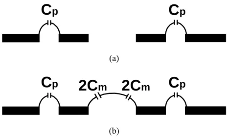
Fig. 2.7 (a) Even- and (b) odd-mode equivalent circuits of the CPW coupled line
length as 2 o p C =C + Cm (2.13a) e C =Cp (2.13b)
The odd- and even-mode characteristic impedances can be expressed as
0o o L Z C =
(2.14a) 0e e L Z C = (2.14b)
The odd- and even-mode phase velocities can be expressed as
_ o p o r eff c V ε = (2.15a) _ e p e r eff c V ε = (2.15b)
where c, and denote the velocity of light, the effective dielectric constants of
odd mode, and the effective dielectric constants of even mode, respectively. _
o r eff
ε εer eff_
The magnitude of the effective dielectric constants is related to the distribution of the electric filed. When the electric field is most in the air, the effective dielectric constant is small and the phase velocity is fast. The odd- and even-mode phases are given
_ o r eff o o p V c ω ω θ = A= A ε (2.16a) _ e r eff e e p V c ω ω θ = A= A ε (2.16b)
We can adjust the geometrical dimensions (S, W, and G) of the CPW coupled line to achieve the desired coupling and make the odd- and even-mode phase velocities close to fit the theory mentioned earlier.
2.2-3 The analysis of the loose-coupling CPW coupler
Coupled lines Top View Ground Ground GroundFig. 2.8 The CPW coupler structure after inserting the ground strip between two coupled lines The CPW coupler structure after inserting the ground strip between two coupled lines is shown in Fig. 2.8. The new structure will change the distribution of the odd- and even-mode electric field, and the variation amount of distribution of even-mode electric field is much more. There are some parts of even-mode electric field attracted to the center ground strip. The new even-mode equivalent circuit is shown in Fig. 2.9 (a). The even-mode characteristic impedance will decrease due to the increased even-mode equivalent capacitance.
C
p
2C
me
2C
me
C
p
Fig. 2.9(a) Even-mode equivalent circuit of the CPW coupled line after inserting the ground
strip between two coupled lines
C
p
2C
mo
2C
mo
C
p
Fig. 2.9 (b) Odd-mode equivalent circuit of the CPW coupled line after inserting the ground strip between two coupled lines
There are some parts of odd-mode electric field attracted to the center ground strip. This will make the odd-mode equivalent capacitance slightly increase. As a result, the odd-mode
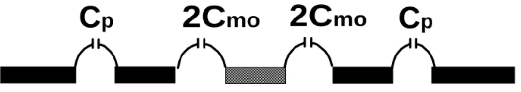
characteristic impedance decreases slightly. The odd-mode equivalent circuit is shown in Fig. 2.9 (b). After inserting the ground strip to the center, the even- and odd-mode characteristic impedances are 0 2 e p m L Z C C = + e (2.17a) 0o 2 p m L Z C C = + o (2.17b)
From (2.10), when the amount of decrease in the even-mode characteristic impedance is larger than the amount of decrease in the odd-mode characteristic impedance, the coupling decreases. The loose-coupling coupler is achieved.
2.2-4 The analysis of the vertically installed planar (VIP) coupler
As described earlier, we know that designing the tight-coupling section is the most difficult portion in the implementation of a multi-section coupler. The tightest coupling of the conventional CPW coupler is about -7 dB, but a tight coupling of -0.77dB is need. Also using a Lange type coupler layout can increase the coupling, it still can not achieve -0.77dB of coupling. Here, we adopt the vertically installed planar (VIP) coupler structure [12] as shown in Fig. 2.10. VIP substrate Main substrate (b) VIP substrate Main substrate Metal (a) Ground
Fig. 2.11 (a) Even- and (b) odd-mode equivalent circuits of the VIP structure
The VIP substrate stands vertically on the main substrate. Both metals on the VIP substrate act as a broadside-coupled lines giving the tight coupling to achieve our need.
The even- and odd-mode equivalent circuits of the VIP structure are shown in Fig. 2.11, where a magnetic wall and an electric wall are located at the symmetrical planes respectively.
The odd-mode equivalent capacitors contain CP and 2Cm. Because the distance (4 mil)
between the symmetrical plane and the signal conductor is very small, the capacitance 2Cm is
much larger than capacitance CP. Therefore, the capacitor 2Cm is the major term. We can
adjust the metal widths on the VIP substrate to fit the desired odd-mode characteristic impedance and adjust the distance between the ground and the VIP substrate to fit the desired even-mode characteristic impedance. In the odd-mode excitation, the electric field is mostly
confined in the VIP substrate (εr =3.38). In the even-mode excitation, most of electric field
is in the air (εr =1). Therefore, the VIP structure has inherently different odd- and even-mode
phase velocities. We know the phase velocities are related to the effective dielectric constants given by (2.15a), (2.15b). Therefore, the odd-mode phase velocity is slower than even-mode phase velocity. The problem needs to be solved, otherwise the isolation is bad and the
both sides of the VIP substrate as shown in Fig. 2.12. VIP substrate Main substrate Dielectric block
Fig. 2.12The compensated VIP structure with dielectric blocks (εr =3.38)
After compensating the circuit, the effective dielectric constants of odd and even mode can be much closer. As a result, the odd- and even-mode phase velocities can be nearly equal.
2.3 Design procedure and Simulation
From Table 2.1, we obtain the design parameter such as odd- and even-mode characteristic impedances and coupling. We adopt the symmetrical structure due to its advantage mentioned earlier. For structural symmetry, the 5-section coupler has 3 different
coupled-line sections. The 90o phase difference between coupled port and through port should
be independent of number of sections. If each section is fitted to Table 2.1, we can achieve the desired specifications. In order to shrink the circuit size and increase the coupling, we choose the high dielectric substrate (εr =9.8) with 15 mil thickness and the VIP substrate (εr =3.38) with 8 mil thickness, respectively.
2.3-1 The loose-coupling section (section 1 and section 5)
From Table 2.1, we see the section 1 and section 5 are loose-coupling structure (-15.35dB of coupling). The CPW loose coupled-line structure in Fig. 2.8 is used. This structure reduces not only the coupling but also the circuit area. One more advantage is that the strip width of the second section coupled-line is nearly the same with this loose
coupled-line structure. Therefore using this loose coupled-line structure has less junction-discontinuity effect.
The design targets of the loose-coupling section (S1&S5) are Zoe=59.411 Ω ,
Zoo=42.08Ω and coupling= -15.35 dB. Roughly calculate the gap, spacing, width and the
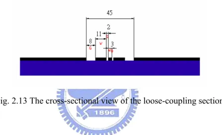
coupled line length. Then, use EM simulator such as Sonnet to simulate the circuit. Slightly adjust the physical dimensions of the circuit to fit the values of Zoo and Zoe and to obtain the desired coupling (-15.35dB) at center frequency 10GHz. The cross-sectional view of the loose-coupling section is shown in Fig. 2.13.
Fig. 2.13 The cross-sectional view of the loose-coupling section
The even- and odd-mode excitations are shown in Fig. 2.14 (a) and (b). Fig. 2.15 (a) shows the simulated results (S parameters) using EM simulator such as Sonnet. Fig. 2.15 (b) shows the even- and odd-mode phases.
1 2 3 4 SUBCKT ID=S2 NET="Z1" PORT P=1 Z=zz Ohm PORT P=2 Z=zz Ohm zoe=59.41 zz=zoe/2 (a)
o o o n1 : 1 n2 : 1 1 2 3 4 5 XFMRTAP ID=X1 N1=0.707 N2=0.707 o o o n1:1 n2:1 1 2 3 4 5 XFMRTAP ID=X2 N1=0.707 N2=0.707 1 2 3 4 SUBCKT ID=S1 NET="Z1" PORT P=3 Z=zoo Ohm PORT P=4 Z=zoo Ohm zoo=42.08 (b)
Fig. 2.14 (a) Even- and (b) odd-mode excitations
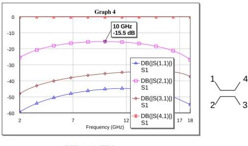
2 7 12 17 18 Frequency (GHz) Graph 4 -60 -50 -40 -30 -20 -10 0 10 GHz -15.5 dB DB(|S(1,1)|) S1 DB(|S(2,1)|) S1 DB(|S(3,1)|) S1 DB(|S(4,1)|) S1 1 2 3 4
Fig. 2.15 (a) The simulated results of the loose-coupling section
2 7 12 17 18 Frequency (GHz) Graph 2 -180 -140 -100 -60 -20 0 10 GHz -91.38 Deg 10 GHz -89.4 Deg Ang(S(2,1)) (Deg) Schematic 1 Ang(S(4,3)) (Deg) Schematic 1
From Fig. 2.15 (a) the simulated coupling -15.5dB almost equals the desired coupling -15.35dB. From Fig. 2.15 (b) the even- and odd-mode phases are near 90 degree.
2.3-2 The middle-coupling section (section 2 and section 4)
The coupling of the section 2 and section 4 are both -7.24dB. We use the conventional CPW coupled lines as shown in Fig. 2.6 to implement. The design of this coupled-lined section is much easier than the others. We obtain the physical dimensions of the CPW coupled line by keying the values of Zoo, Zoe and electrical length by ADS LineCal.
The design targets of the middle-coupling section (S2&S4) are Zoe=79.63 Ω ,
Zoo=31.40Ω and coupling= -7.24 dB. The gap, line width, and the coupled line length are
firstly obtained from the ADS LineCal. Then, use EM simulator such as Sonnet to simulate the circuit. Slightly adjust physical dimensions of the circuit to fit the values of Zoo and Zoe and to obtain the coupling (-7.24dB) at center frequency 10GHz. The cross-sectional view of the middle-coupling section is shown in Fig. 2.16.
2 7 12 17 18 Frequency (GHz) Graph 1 -60 -50 -40 -30 -20 -10 0 10 GHz -7.392 dB 1 2 3 4 DB(|S(1,1)| S2 ) DB(|S(2,1)| S2 ) DB(|S(3,1)| S2 ) DB(|S(4,1)|) S2
Fig. 2.17 (a) The simulated results of the middle-coupling section
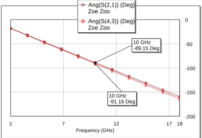
2 7 12 17 18 Frequency (GHz) Graph 2 -200 -150 -100 -50 0 10 GHz -91.16 Deg 10 GHz -89.15 Deg Ang(S(2,1)) (Deg) Zoe Zoo Ang(S(4,3)) (Deg) Zoe Zoo
Fig. 2.17 (b) Even- and odd-mode phases of the middle-coupling section
Fig. 2.17 (a) shows the simulated results (S parameters) using Sonnet. The simulated coupling -7.392dB almost equals the wanted coupling -7.24dB. Fig. 2.17 (b) shows the even- and odd-mode phases of the middle-coupling section. The even- and odd-mode phases are near 90 degree.
2.3-3 The tight-coupling section (center section)
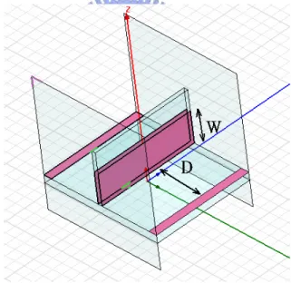
The VIP structure is a 3D structure that a 3D EM simulator such as HFSS is used to simulate. Because there is no analytic method for analyzing the VIP coupler, trial-and-error method is used to obtain the solution. According to equations (2.14a), (2.14b), a high even-mode characteristic impedance can be obtained by moving the CPW ground strip far away from the VIP substrate because the equivalent even-mode capacitance decreases as the distance between signal strips and CPW ground strips increases. A lower odd-mode characteristic impedance can be achieved by increasing the widths of the metal strips on both sides of the VIP substrate because the equivalent odd-mode capacitance increases as the widths of the metal strips increase. We follow the rule to try the solution. 3D view of the final solution of the VIP structure is shown in Fig. 2.18 where W is 60 mil and D is 100 mil.
Fig. 2.18 3D diagram of the VIP structure in HFSS
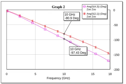
Fig. 2.19 (a) and (b) show the simulated S parameters, the even- and odd-mode phases, respectively. At the center frequency 10GHz, the coupling fits our need, but the phase difference between the even- and odd-mode is large. The phase difference is about 17 degree at 10GHz.
2 7 12 17 18 Frequency (GHz) Graph 1 -40 -30 -20 -10 0 10 GHz -0.7709 dB DB(|S(1,1)|) VIP DB(|S(2,1) VIP |) 1 2 3 4 DB(|S(3,1) VIP |) DB(|S(4,1) VIP |)
Fig. 2.19 (a) The simulated results of the tight-coupling section
0 5 10 15 18 Frequency (GHz) Graph 2 -200 -150 -100 -50 0 10 GHz -97.43 Deg 10 GHz -80.9 Deg Ang(S(4,3)) (Deg) Zoe Zoo Ang(S(2,1)) (Deg) Zoe Zoo
Fig. 2.19 (b) Even- and odd-mode phases of the tight-coupling section
We compensate the phase difference by putting the dielectric blocks (εr =3.38) at both
sides of the VIP substrate as shown in Fig. 2.20. The odd- and even-mode phase velocities are equalized by adjusting the size of dielectric blocks. The simulated results are shown in Fig. 2.21 (a) and (b).
) 38 . 3 ( r = block Dielectric ε ) 38 . 3 ( r = block Dielectric ε
Fig. 2.20 The compensated VIP structure
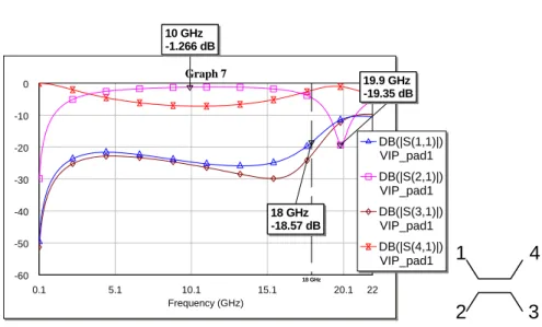
0.1 5.1 10.1 15.1 20.1 22 Frequency (GHz) Graph 7 -60 -50 -40 -30 -20 -10 0 18 GHz 18 GHz -18.57 dB 10 GHz -1.266 dB 19.9 GHz -19.35 dB DB(|S(1,1)|) VIP_pad1 DB(|S(2,1)|) VIP_pad1 DB(|S(3,1)|) VIP_pad1 DB(|S(4,1)|) VIP_pad1 1 2 3 4
Fig. 2.21 (a) The simulated results of the compensated tight-coupling section
0.1 5.1 10.1 15.1 19 Frequency (GHz) Graph 1 -200 -150 -100 -50 0 10 GHz -91.51 Deg 10 GHz -87.99 Deg Ang(S(2,1)) (Deg) Schematic 1 Ang(S(4,3)) (Deg) Schematic 1
Fig. 2.21 (b) Even- and odd-mode phases of the compensated tight-coupling section From Fig. 2.21 (b), we see that difference between the even- and odd-mode phases are
much smaller and close to 90o at the center frequency. The dielectric blocks (εr =3.38) increase the even-mode capacitance, so the even-mode characteristic impedance decreases. As a result, the coupling decreases. The coupling is about 0.5dB decrease from the original value.
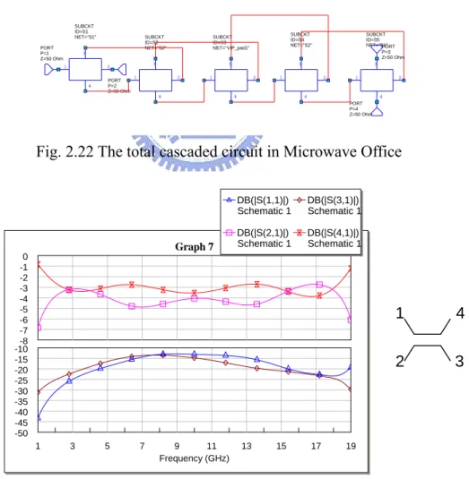
2.3-4 The total cascaded circuit
Now, we have finished the design of each section, so we can cascade them one by one as shown in Fig. 2.22. We can first simulate the cascaded response by Microwave Office. The simulated results are shown in Fig. 2.23. We can see that the performance of the cascaded circuit is good from 2.2~18.2GHz. It saves much time to simulate the cascaded circuit by circuit simulator. Though the simulated results are less accurate, it still gives a good initial design. 1 2 3 4 SUBCKT ID=S1 NET="S1" 1 2 3 4 SUBCKT ID=S2 NET="S2" 1 2 3 4 SUBCKT ID=S3 NET="VIP_pad1" 1 2 3 4 SUBCKT ID=S4 NET="S2" 1 2 3 4 SUBCKT ID=S5 NET="S1" PORT P=1 Z=50 Ohm PORT P=2 Z=50 Ohm PORT P=3 Z=50 Ohm PORT P=4 Z=50 Ohm
Fig. 2.22 The total cascaded circuit in Microwave Office
1 3 5 7 9 11 13 15 17 19 Frequency (GHz) Graph 7 -50 -45 -40 -35 -30 -25 -20 -15 -10-8 -7 -6 -5 -4 -3 -2 -1 0 DB(|S(1,1)|) Schematic 1 DB(|S(2,1)|) Schematic 1 DB(|S(3,1)|) Schematic 1 DB(|S(4,1)|) Schematic 1 1 2 3 4
Fig. 2.23 The simulated results by Microwave Office
as shown in Fig. 2.24. The simulated results are shown in Fig. 2.25 to see the influence of the S3. Fig. 2.25 shows that the simulated results are very close to an ideal 5-section coupler. We confirm that the design of the other sections except S3 satisfies our need.
W W 1 2 3 4 CLIN ID=TL1 ZE=237.1 Ohm ZO=10.54 Ohm EL=90 Deg F0=10 GHz 1 2 3 4 SUBCKT ID=S1 NET="S1" 1 2 3 4 SUBCKT ID=S2 NET="S2" 1 2 3 4 SUBCKT ID=S4 NET="S2" 1 2 3 4 SUBCKT ID=S5 NET="S1" PORT P=1 Z=50 Ohm PORT P=2 Z=50 Ohm PORT P=3 Z=50 Ohm PORT P=4 Z=50 Ohm Ideal S3
Fig. 2.24 The total modified cascaded circuit in Microwave Office
1 3 5 7 9 11 13 15 17 19 Frequency (GHz) Graph 8 -50 -45 -40 -35 -30 -25 -20 -15 -10-8 -7 -6 -5 -4 -3 -2 -1 0 DB(|S(1,1)|) Schematic 2 DB(|S(2,1)|) Schematic 2 DB(|S(3,1)|) Schematic 2 DB(|S(4,1)|) Schematic 2 1 2 3 4
Fig. 2.25 The modified simulated results by Microwave Office
Finally, we simulate the whole 5-section coupler by an EM simulator such as HFSS to get more accurate results. The 3-D structure of the whole 5-section coupler is shown in Fig. 2.26. Fig. 2.27 (a) shows the simulated results by HFSS. The useful bandwidth is from 2 to 16 GHz. The maximal amplitude error between the coupled and through port within the bandwidth is about 3.6 dB. Fig. 2.27 (b) shows the phases of the coupled and through port.
The phase error is up to about 15o at 15.5 GHz. Compare Fig. 2.27 (a) with Fig. 2.23, the
performance degradation is mainly from the junction discontinuity effect between each section, especially between section 3 and its neighbors.
Fig. 2.26 The total circuit in HFSS 0 2 4 6 8 10 12 14 16 18 20 Frequency (GHz) Graph 1 -40 -35 -30 -25 -20 -15 -10 -5 -10 -9 -8 -7 -6 -5 -4 -3 -2 -10 DB(|S(1,1)|) Total_F DB(|S(2,1)|) Total_F DB(|S(3,1)|) Total_F DB(|S(4,1)|) Total_F 1 2 3 4
Fig. 2.27 (a) The simulated results of the total circuit by HFSS
0 5 10 15 20 Frequency (GHz) Graph 2 -200 -100 0 100 200 2 GHz -46.41 Deg 2 GHz -136.4 Deg 16 GHz 43.32 Deg 16 GHz 158.7 Deg 18 GHz 9 GHz -130.6 Deg 9 GHz 139.2 Deg Ang(S(2,1)) (Deg) Total_F Ang(S(4,1)) (Deg) Total_F
2.4 Circuit fabrication and Measurement
(a) (b)
Fig. 2.28 Photos of (a) the fabricated 5-section hybrid coupler and (b) the fabricated 5-section hybrid coupler with dielectric blocks
Based on the previously mentioned design procedures, the proposed 5-section hybrid coupler is fabricated. The photos of the proposed 5-section hybrid coupler are shown in Fig. 2.28. The circuit size is 16.8mm × 6mm and the dielectric blocks at each side of VIP are with the size of 2.5mm × 2.5mm. The thickness of the dielectric block is 60mil.
The measured results of the whole 5-section coupler without dielectric blocks are shown in Fig. 2.29 (a). We see the performance is bad as frequency goes high. Fig. 2.29 (b) shows the phases of the coupled and through port. Fig. 2.29 (c) depicts the amplitude and phase errors between the coupled and through port. The phase error is keeping at 90 -8/+3 degree over the designed frequency of 2-18 GHz. The maximal amplitude error is up to 6.8 dB at 16 GHz and it does not meet the hybrid specifications.
0 2 4 6 8 10 12 14 16 18 20 Frequency (GHz) Graph 3 -50 -45 -40 -35 -30 -25 -20 -15 -10 -5 -11 -10-9 -8 -7 -6 -5 -4 -3 -2 -10 DB(|S(2,1)|) aircoup DB(|S(2,1)|) airiso DB(|S(2,1)|) airthr DB(|S(1,1)|) airthr
0 5 10 15 20 Frequency (GHz) Graph 2 -200 -100 0 100 200 10 GHz 141.4 Deg 10 GHz -133.8 Deg Ang(S(2,1)) (Deg) aircoup Ang(S(2,1)) (Deg) airthr
Fig. 2.29 (b) Phases of the coupled and through port
0 2 4 6 8 10 12 14 16 18 20 Graph 5 80 85 90 95 100 Phas e error (degree) -4 -3 -2 -10 1 2 3 4 5 6 7 8 Amplitude err o r (dB) PlotCol(1,4) air_measurement PlotCol(1,3) air_measurement
Fig. 2.29 (c) The amplitude and phase errors between the coupled and through port Two dielectric blocks at both sides of the VIP substrate are used to improve central section performance. The measured results of the coupler with dielectric blocks are shown in Fig. 2.30. The amplitudes and phases of the coupled and through port are shown in Fig. 2.30 (a) and (b), respectively. It can be seen that the amplitude error is smaller than that of the circuit without dielectric blocks. The performance of return loss and isolation are also better
than that of the circuit without dielectric blocks. The phase error is smaller than 10o and
0 2 4 6 8 10 12 14 16 18 20 Frequency (GHz) Graph 5 -50 -45 -40 -35 -30 -25 -20 -15 -10 -5 -10 -9 -8 -7 -6 -5 -4 -3 -2 -10 DB(|S(2,1)|) rolargecoup DB(|S(2,1)|) rolargethr DB(|S(2,1)|) rolargeiso DB(|S(1,1)|) rolargethr
Fig. 2.30 (a) The measured results of the total circuit with dielectric blocks
0.045 10.05 20.05 26.5 Frequency (GHz) Graph 2 -200 -100 0 100 200 17 GHz -170.4 Deg 17 GHz 87.83 Deg 2 GHz -127 Deg 2 GHz -39.59 Deg 18 GHz 9.5 GHz 163 Deg 9.5 GHz -114.8 Deg Ang(S(2,1)) (Deg) rolargecoup Ang(S(2,1)) (Deg) rolargethr
Fig. 2.30 (b) Phases of the coupled and through port
0 2 4 6 8 10 12 14 16 18 20 Graph 7 75 80 85 90 95 100 105 Ph as e er ror (d eg re e) -4 -3 -2 -1 0 1 2 3 4 Amp lit ud e er ro r (d B) PlotCol(1,3)
Phase and Amplitude_simulation PlotCol(1,3)
Phase and Amplitude_measurement PlotCol(1,4)
Phase and Amplitude_measurement PlotCol(1,4)
Phase and Amplitude_simulation
Fig. 2.31 The measured and simulated amplitude and phase errors between the coupled and through port
Fig. 2.31 shows the comparison between the measured and simulated amplitude and phase errors. The dotted lines and solid lines are simulated and measured results, respectively. An acceptable agreement between the simulated and measured results is obtained.
Chapter 3
Multilayer Wideband Bandpass Filter
3.1 Introduction
Wideband bandpass filters are the fundamental building blocks for modern broadband wireless communication systems. Bandpass filters in microwave communication systems are often used to eliminate out-band interference signals. This application requires having steep passband-to-stopband transition, high stopband attenuation, wide stopband range and spurious resonant frequencies far away from passband frequency. The microstrip parallel-coupled filter using resonators with half wavelength has been one of the most commonly used filters [14]. This kind of filter has many advantages such as easy design procedures, a wide bandwidth range (from a few percent to more than 40%) and a planar structure. Influenced by the
spurious responses at 2fo, twice the passband frequency, the microstrip parallel-coupled filter
may seriously diminish the attenuation of the upper stopband as the bandwidth gets wider. Stepped impedance resonators (SIR) are composed of transmission lines with different characteristic impedances. They provide an effective way to minimize circuit space and push spurious resonant frequencies away from passband [15]. The resonant frequencies of SIR can be controlled by adjusting the geometrical dimensions, such as the impedance ratio of the high-Z and low-Z segments. Due to the property the first spurious resonant frequency can be
much higher than 2fo, it is useful in wideband bandpass filter application.
A quarter-wavelength resonator filters has the spurious passband at 3f0 instead of 2f0, but
it is still not enough for wideband application [16]. The wiggly-line filter [17] can reject the harmonic passband of the filter by using a continuous perturbation of the width of the coupled lines following a sinusoidal law, but the circuit layout can not achieve wideband filter and is not suitable for suppression of wide spurious passband. Here, we propose the parallel-coupled
filter using half-wave SIR and multi-layer PCB process to realize the wideband bandpass filter.
3.2 Theory
Firstly, the conditions of fundamental and spurious resonance of a half-wave SIR are discussed. The resonator structure to be considered here is shown in Fig. 3.1. The half-wave
SIR is symmetrical and has two different characteristic impedances, Z1 and Z2 in the
resonator. ) ( 2
θ
1θ
2θ
T = + 2θ
2
θ
1θ
2 Z2 Z1 Z2θ
T<
π
)
(
2
θ
1θ
2θ
T=
+
2θ
2
θ
1θ
2 Z2 Z1 Z2π
θ
T>
(a) (b)Fig. 3.1 Structures of the SIR (a) K = Z2/Z1 < 1 (b) K = Z2/Z1 > 1
The admittance Yi of the resonator looking into the open end is
2 1 2 2 2 1 2 2 1 2 1
2 (1 tan )(1 tan ) 2(1 )tan tan
) tan tan )( tan tan ( 2 θ θ θ θ θ θ θ θ K K K K jY Yi + − − − − + = (3.1) where 1 2 Z Z
K = is the impedance ratio. The resonance condition is
Yi =0 (3.2)
From (3.1) and (3.2) at the fundamental resonant frequency we have
K =tanθ1tanθ2 (3.3)
The relationship between θT and θ1 is derived from (3.3) as
) tan tan ( 1 1 2 tan 1 1 θ θ θ + − = K K T (when ≠1 K ) (3.4)
π
θT = (when K =1) (3.5)
When K= 1, this corresponds to a uniform impedance resonator (UIR). The resonator length T
θ has minimal value when 0 <K< 1 and maximal value when K> 1. This condition can be
obtained by differentiating (3.4) by θ1, 0 sin ) (tan 1 1 1 2 1 2 − = −K θ K θ (3.6) then tan 1( ) 1 K − = θ (3.7)
The above equation is the condition that θT has the maximal or minimal value for constant
K. For practical application it is preferable to choose θ1 = because the design equations θ2
can be simplified considerably. Therefore, in the following discussion, the SIR is treated as
having θ1 =θ2 =θ, and (3.1) can be expressed as
θ θ θ θ 4 2 2 2 2 tan tan ) 1 ( 2 tan ) tan )( 1 ( 2 K K K K K K jY Yi + + + − − + = (3.8)
The resonance condition is then given, using the fundamental frequency f0 and corresponding
length θ0, as K = 0 2 tan θ or ) ( tan 1 0 K − = θ (3.9)
Taking the spurious resonance frequency to be fsn (n =1, 2, 3,…) and corresponding θ
with θsn (n = 1,2,3,…), we obtain from (3.8) and (3.2)
0 tan 0 tan tan 3 2 2 1 = = − ∞ = s s s K θ θ θ (3.10)
⎟⎟ ⎠ ⎞ ⎜⎜ ⎝ ⎛ = = − ⎟⎟ ⎠ ⎞ ⎜⎜ ⎝ ⎛ = = = = − 0 1 0 3 0 3 0 1 0 2 0 2 1 0 1 0 1 2 1 2 tan 2 f f f f f f f f K f f s s s s s s s s θ θ θ θ π θ θ (3.11)
The above results are all a function of the impedance ratio K. Hence, the spurious response can be controlled by the choice of the impedance ratio K, which is a key feature of this type of filter. We can utilize the low impedance ratio K to push the spurious response to high frequency and the length of the resonator will be shortened. The above equations neglect the physical step discontinuity effect at the junction of the two lines.
Next, we consider a parallel coupled transmission line with arbitrary length and its equivalent circuit. For designing bandpass filters with SIR in which lines are coupled in parallel, it is necessary to find the relationship between even- and odd-mode characteristic impedances in the parallel coupled sections and the admittance inverter parameters. Fig. 3.2 (a) shows even- and odd-mode characteristic impedances Zoe, Zoo of a coupled line of electrical
length θ , and its equivalent circuit is expressed by two single transmission lines of electrical
length θ , impedance Zo and admittance inverter parameter J as shown in Fig. 3.2 (b)
θ Zoe, Zoo J -90o θ θ (a) (b)
Fig. 3.2 (a) Parallel coupled line and (b) its equivalent circuit The ABCD matrix for Fig. 3.2 (a) and (b) can be expressed as
[ ]
(
) (
)
(
)
⎥ ⎥ ⎥ ⎥ ⎦ ⎤ ⎢ ⎢ ⎢ ⎢ ⎣ ⎡ − + − − + + − − + = θ θ θ θ θ cos sin 2 sin 2 cos cos 2 2 2 oo oe oo oe oo oe oo oe oo oe oo oe oo oe oo oe a Z Z Z Z Z Z j Z Z Z Z Z Z j Z Z Z Z F (3.12)[ ]
⎥ ⎥ ⎥ ⎥ ⎥ ⎦ ⎤ ⎢ ⎢ ⎢ ⎢ ⎢ ⎣ ⎡ ⎟⎟ ⎠ ⎞ ⎜⎜ ⎝ ⎛ + ⎟⎟ ⎠ ⎞ ⎜⎜ ⎝ ⎛ − ⎟⎟ ⎠ ⎞ ⎜⎜ ⎝ ⎛ − ⎟⎟ ⎠ ⎞ ⎜⎜ ⎝ ⎛ + =θ
θ
θ
θ
θ
θ
θ
θ
cos sin 1 cos sin cos sin cos sin 1 2 2 2 2 2 2 o o o o o o b JZ JZ J JZ j J JZ j JZ JZ F (3.13)Then equalizing each corresponding matrix element
[ ] [ ]
Fa = Fb , we can obtainθ θ θ 1 sin cos cos ⎟⎟ ⎠ ⎞ ⎜⎜ ⎝ ⎛ + = − + o o oo oe oo oe JZ JZ Z Z Z Z (3.14)
(
) (
)
(
Z Z)
JZ J Z Z Z Z o oo oe oo oe oo oe θ θ θ θ 2 2 2 2 2 2 cos sin sin 2 cos − = − + + − (3.15) θ θ θ 2 2 2 cos sin sin 2 J JZ Z Zoe oo o − = − (3.16)The above simultaneous equations are not independent of each other, and any two equations among the three are valid for solution. Solving (3.14) and (3.16), we obtain
θ θ 2 2 2 cot 1 csc 1 ⎟⎟ ⎠ ⎞ ⎜⎜ ⎝ ⎛ − ⎟⎟ ⎠ ⎞ ⎜⎜ ⎝ ⎛ + + = o o o o oe Y J Y J Y J Z Z (3.17) θ θ 2 2 2 cot 1 csc 1 ⎟⎟ ⎠ ⎞ ⎜⎜ ⎝ ⎛ − ⎟⎟ ⎠ ⎞ ⎜⎜ ⎝ ⎛ + − = o o o o oo Y J Y J Y J Z Z (3.18)
These are generalized expressions for parallel coupled lines with arbitrary length. In the special case of quarter-wavelength coupling, by considering the situation
2
π
θ = in (3.17)
2 1 ⎟ ⎠ ⎞ ⎜ ⎝ ⎛ + ⎟ ⎠ ⎞ ⎜ ⎝ ⎛ + = K Z K Z Z Z o o o oe (3.19) 2 1 ⎟ ⎠ ⎞ ⎜ ⎝ ⎛ + ⎟ ⎠ ⎞ ⎜ ⎝ ⎛ − = K Z K Z Z Z o o o oo (3.20) where o o Y J K
Z = (K is impedance inverter parameter ).
The fundamental configuration of n-stage bandpass filter considered here is shown in Fig.
3.3, and slope parameters for all resonators are of equal value, b(b=2θ0Yo). When element
values gj and relative bandwidth w are given as fundamental design parameters of a bandpass
filter, the admittance inverter parameter Jj,j+1, can be expressed as
1 0 1 1 1 , 1 0 1 1 1 , 1 0 0 1 0 1 01 2 2 2 + + + + + + + = = = = = = n n o j j o n n j j o j j j j j j o o g g w Y g g w b Y J g g w Y g g b b w J g g w Y g g w b Y J θ θ θ
(j=1~n-1) (3.21)
θ
2θ
θ
Zo Zo Z1 Z1 (Zoe)01 (Zoo)01 (Zoe)12 (Zoo)12 (Zoe)23 (Zoo)23 (Zoe)n,n+1 (Zoo)n,n+1Fig. 3.3 Bandpass filter using SIR structure
Using (3.17) and (3.18) in the previous section, the design data for coupled lines can be obtained. It is then possible to design a bandpass filter as a SIR structure.
3.3 Design procedure and Simulation
The circuit model of a parallel coupled-line describe above is only good for relatively narrowband and is not suitable for wideband (fractional bandwidth >30%) filter. The fractional bandwidth of the proposed filter is 66.67% (2-4 GHz). The above method has significant errors.
We utilize the optimization to design the wideband filter. Using the optimization saves our time without analyzing the complicated mathematical formulas to obtain circuit parameters such as impedances and effective dielectric constants etc. The optimization procedures are described as follows. Firstly, we construct the filter model of center frequency 3 GHz and passband 2-4 GHz in Microwave Office. Then, utilize the optimization to obtain the design parameters shown in Fig. 3.4. Fig. 3.5 depicts the simulated wideband bandpass filter response. The first spurious resonant frequency is pushed to about 3.8 times passband frequency. W W 1 2 3 4 CLINP ID=TL1 ZE=Zoe1 Ohm ZO=Zoo1 Ohm L=L1 mil KE=ke1 KO=ko1 AE=0 AO=0 W W 1 2 3 4 CLINP ID=TL2 ZE=Zoe2 Ohm ZO=Zoo2 Ohm L=L3 mil KE=ke2 KO=ko2 AE=0 AO=0 W W 1 2 3 4 CLINP ID=TL3 ZE=Zoe2 Ohm ZO=Zoo2 Ohm L=L3 mil KE=ke2 KO=ko2 AE=0 AO=0 W W 1 2 3 4 CLINP ID=TL4 ZE=Zoe1 Ohm ZO=Zoo1 Ohm L=L1 mil KE=ke1 KO=ko1 AE=0 AO=0 TLINP ID=TL5 Z0=Z1 Ohm L=L2 mil Eeff=er1 Loss=0 F0=0 GHz TLINP ID=TL7 Z0=Z1 Ohm L=L2 mil Eeff=er1 Loss=0 F0=0 GHz TLINP ID=TL6 Z0=Z2 Ohm L=L4 mil Eeff=er2 Loss=0 F0=0 GHz PORT P=1 Z=50 Ohm PORT P=2 Z=50 Ohm L2=144 L4=197 ko1=3.1 ke1=1.84 ko2=3.15 ke2=2.4 Z1=193 er1=1.718 Z2=193 er2=1.718 Zoe1=97 Zoo1=10 Zoe2=51 Zoo2=8.3 L1=302 L3=210
0 2 4 6 8 10 12 14 16 18 20 Frequency (GHz) Graph 1 -60 -50 -40 -30 -20 -10 0 DB(|S(1,1)|) Schematic 1 DB(|S(2,1)|) Schematic 1
Fig. 3.5 The wideband bandpass filter response
From the design parameters, we see that high and low impedances of even mode are needed. We propose multilayer broadside coupling structure to achieve high even-mode and low odd-mode characteristic impedances. Fig. 3.6 depicts the proposed 3-layer structure. The 3 layers of metal are the ground metal in the middle layer and signal lines at two outer layers of metal, respectively. Where W is the width of the signal line and G is the overlap (negative symbol) or gap (positive symbol) between ground metal and signal lines.
We can utilize the odd- and even-mode excitations to analyze the structure due to its symmetrical structure. In the odd-mode excitation, we set the middle plane as an electric wall to simplify simulation. We use the same method to solve the even-mode excitation, but set the middle plane as a magnetic wall. Fig. 3.7 shows the odd- and even-mode equivalent circuits. We can obtain the characteristic impedances and effective dielectric constants of odd and even mode from the simulated results.
8mil 8mil W W G G 8mil 8mil W W G G
Fig. 3.6 3-layer structure
(a) (b) W G Electric wall 8mil Co W G Magnetic wall Ce 8mil
Fig. 3.7 (a) Odd-mode and (b) even-mode equivalent circuits
Odd- and even-mode characteristic impedances are expressed as
o oo C L Z = , e oe C L Z = (4.21)
Fig. 3.8 shows the 3D diagram of even- and odd-mode circuits in HFSS. The substrate thickness and relative dielectric constant are 8mil and 3.38, respectively. We set the width of the high characteristic impedance line as 10 mil for easy fabrication. The simulated results are shown in Fig. 3.9(a)-(e). It can be observed in Fig. 3.9 (a) that even-mode characteristic impedances increase as G increases and W decreases. Because increase G and decrease W, reduce the even-mode equivalent capacitances (Ce).
Ground Symmetrical plane
Coupled line
Fig. 3.8 The 3D diagram of even- and odd-mode excitations in HFSS
-20 -10 0 10 20 30 0 50 100 150 200 250 300 Zoe (ohm) G (mil) W (mil) 10 30 50 70 90 110 130 150 170 190 210
Fig. 3.9 (a) Even-mode characteristic impedances versus G and W
-20 -10 0 10 20 30 1.2 1.4 1.6 1.8 2.0 2.2 2.4 2.6 2.8 εre G (mil) W (mil) 10 30 50 70 90 110 130 150 170 190 210
Fig. 3.9 (b) depicts that the even-mode effective dielectric constant increases as G and W decrease. Because smaller G and W attract more electric field in the substrate, the even-mode effective dielectric constant increases. For the same reason, we can explain Fig. 3.9 (c)-(e). It should be point out that the characteristic impedances and effective dielectric constants of odd-mode are less influenced by parameter G. From Fig. 3.7 (a), we see the middle plane is electric wall that is similar to a ground plane, so parameter G has less influence on the result.
-20 -10 0 10 20 30 5 10 15 20 25 30 35 40 45 50 55 60 65 70 75 80 Zoo (ohm) G (mil) W (mil) 10 30 50 70 90 110 130 150 170 190 210
Fig. 3.9 (c) Odd-mode characteristic impedances versus G and W
-20 -10 0 10 20 30 2.50 2.55 2.60 2.65 2.70 2.75 2.80 2.85 2.90 2.95 3.00 3.05 3.10 3.15 εro G (mil) W (mil) 10 30 50 70 90 110 130 150 170 190 210
0 20 40 60 80 100 120 140 160 180 200 220 Zoh εrh G (mil) Z oh (ohm) 1.5 1.6 1.7 1.8 1.9 2.0 2.1 2.2 2.3 2.4 ε rh
Fig. 3.9 (e) Characteristic impedances and effective dielectric constants of the high impedance line versus G
According to the simulated results, we can obtain the desired geometrical dimensions. The circuit diagram in EM simulator HFSS is shown in Fig. 3.10. There are step-junction and open-end effects that affect responses of the circuit. Therefore, the circuit has to be finely tuned. The final geometrical dimensions of the wideband bandpass filter are shown in Table 3.1 and the simulated results are shown in Fig. 3.11.
Fig. 3.10 (b) Cross-sectional view of the wideband bandpass filter diagram
W1 G1 L1 W2 G2 L2 W3 G3 L3 W4 G4 L4 W50 H50
150 0 240 10 53 144 180 -14 174 10 53 197 18 200
Table 3.1 The geometrical dimensions of the wideband bandpass filter (unit: mil)
Fig. 3.11 Simulated results of the wideband bandpass filter
From Fig. 3.11, we see that the filter bandwidth is slightly reduced. In the tuning process, we have to trade off between the passband return loss and bandwidth. We sacrifice some bandwidth for better return loss.
3.4 Circuit fabrication and Measurement
Fig. 3.12 shows the photos of the multilayer wideband bandpass filter. The circuit size is 1313 mil×366 mil (33.4mm×9.3 mm).
(a) Front-side view
(b) Back-side view
Fig. 3.12 (a) Front-side view and (b) back-side views of the circuit photos
From the circuit photos, we see that the two substrates are fixed by six screws. This can cause fabrication errors because the six screws can not fix every part of the two thin substrates
very tightly. The measured and simulated results are both shown in Fig. 3.13 for comparison. The solid and dotted lines are measured and simulated results, respectively. The measured and simulated results are matched well, except the measured passband return loss is not as well as the simulated one. The return loss degradation might come from the fabrication errors. The fabrication errors include air gaps between two screw-fastened substrates and misalignment of the circuit. A very wide upper stopband clearance of -23dB up to 20GHz is achieved. Fortunately, the spurious response at 13GHz in the measured results is not as high as the results in the simulation.
0.01 2 4 6 8 10 12 14 16 18 20 Frequency (GHz) Graph 1 -60 -50 -40 -30 -20 -10 0 DB(|S(1,1)|) measurement DB(|S(2,1)|) measurement DB(|S(2,1)|) simulation DB(|S(1,1)|) simulation
Chapter 4
Conclusion
This thesis has demonstrated two kinds of microwave circuits namely, multi-section ultra-broadband quadrature hybrid coupler and multilayer wideband bandpass filter.
In chapter 2, miniaturized ultra-broadband quadrature hybrid coupler has been realized by using 5-section cascaded CPW coupler structure. The synthesis techniques based on the concept of odd- and even-mode analysis has been developed. The VIP structure to achieve a extremely tight of coupling has been proposed. The unequal modal phase velocities, however, are a serious problem in the VIP structure. Putting two dielectric blocks with the same dielectric constant as the VIP substrate at both sides of the VIP substrate to compensate the modal phase velocities of a VIP coupled-line has been successfully developed. Although two dielectric blocks improve the directivity, they lower the even-mode characteristic impedance. Tradeoff between directivity and coupling should be made. Finally, the measured results have shown a good agreement with the simulated results. The bandwidth reduction mainly results from the insufficient even-mode characteristic impedance in the tight-coupling section, the discontinuities between each section, and the air gaps between the dielectric blocks and VIP substrate. There still has space to improve the performance.
In chapter 3, the wideband bandpass filter has been realized by using the parallel coupled stepped impedance resonators (SIR). Utilizing the SIR to push the spurious frequency far away from the passband center frequency has been successfully developed. The multilayer structure to achieve a high to low even-mode characteristic impedances has been proposed. According to the design parameters from the simulated results, a wideband bandpass filter can be easily designed. Finally, the measured and simulated results have been matched well. A very wide upper stopband clearance of -23dB up to 20GHz has been achieved.