Growth process of Ge on Si
„100…-„231… in atomic-layer epitaxy from Ge
2H
6 Kuang-Hsin Huang, Tsai-Shian Ku, and Deng-Sung LinInstitute of Physics, National Chiao-Tung University, 75 Bo-Ai Street, Hsinchu, Taiwan
~Received 21 October 1996!
This study investigates the growth process of Ge on Si~100! during atomic-layer epitaxy ~ALE! utilizing digermane. The surface ordering, morphology, and stoichiometry of the digermane saturated Si~100! surface at temperatures between 300 and 900 K, as well as the grown films are examined both by scanning tunneling microscopy~STM! and high-resolution core-level photoemission spectroscopy employing synchrotron radia-tion. An exposure of more than 15 L~1 L51026 T s! of digermane on the Si~100!-(231) surface at room-temperature results in a saturated and disordered surface. When the digermane saturated surface is heated to 725 K for 60 s, diluted Ge dimer chains are created and surrounded by SiH species. Further annealing to 810 K completely desorbs hydrogen from the surface, leaving large two-dimensional islands covering;41% of its area. The surface recovers its smooth 231 structure, but is interspersed with poorly ordered short dimer vacancy lines at 900 K with no observable contrast on the atomic terraces, indicating displacive adsorption of Ge on the terraces. Significant differences of the surface diffusion phenomena between the gas-phase and solid-phase molecular-beam epitaxy~MBE! are observed. Multilayer Si deposition is performed by ALE, i.e., cyclic digermane adsorption at near room temperature, followed by thermal annealing at 900 K. STM images reveal the formation of 23n structures and increasing roughening of the surface as the growth cycle increases, similar to what occurs during MBE. Issues related to the atomic origins of surface core-level shifts and the chemical composition of the surface layer resulting from the formation of mixed Ge-Si or Ge-Ge during the submonolayer adsorption of Ge on Si~100! are also discussed. @S0163-1829~97!05832-3#
I. INTRODUCTION
Surface processes during chemical vapor deposition
~CVD! and the atomic-layer epitaxy ~ALE! of group-IV
ele-ments currently have received extensive interest.1–8 As the trend toward reducing device dimensions continues, submi-crometer Si technology places increasingly stringent de-mands on thin-film techniques. One of the most significant developments has been the introduction of ALE. This cyclic vapor-phase epitaxial film growth technique incorporates self-limiting kinetic processes which result in the deposition of quantized thickness per growth cycle. Because its deposi-tion rate is kinetically self-limiting, ALE has proven itself a highly effective technique for improving crystalline quality and layer thickness uniformity.1,9 Its cyclic deposition pro-cess facilitates the growth of materials with extremely nar-row single or alternative doping spikes for quantum-layer devices.
An example is Si ALE on Si~100!-(231) with disilane as the gas source.1 On exposure to more than 10 L of disilane, the Si~100!-(231) surface adsorbs a nominal 0.5 ML ~1
ML56.7831014 cm22) of dissociated fragments~SiH3
tri-hydride and SiH2 dihydride! at ,400 K. Since the hydrides
saturate all the surface dangling bonds, the sticking probabil-ity of any excess disilane is essentially zero, the Si~100! surface is passive to further disilane exposure, and the disi-lane flow is then halted. Once the surface is heated to a high temperature or irradiated with UV laser pulses to desorb H, the net deposition is;0.5 ML. Repeating this growth cycle, first saturating the Si~100! surface with disilane, followed by high-temperature annealing, results in a quantized ~0.5 ML layer per cycle! deposition of Si. Because the surface, rather than the supply of gas source, controls the growth via the
self-limiting process, only a single layer or less is deposited in each cycle which can result in low defect density and satisfactory layer thickness uniformity.
This study reports the findings of an investigation conducted by a combination of scanning tunneling
micros-copy ~STM! and synchrotron core-level photoemission into
Ge ALE on Si~100!-(231) utilizing digermane. Chemi-cally similar to Si2H6 ~disilane!, Ge2H6 ~digermane!
func-tions as excellent precursor molecules for Ge growth.4,7 It exhibits high sticking probability (;0.5) on Si and Ge surfaces and its lower decomposition activation energy for both gas phases and surface reactions allows a lower depo-sition temperature. The heteroexpitaxy of Si and Ge on each other is of relevance both to fundamental thin-film science and to the potential applications of Si12xGex
heterostruc-tures and Si/Si12xGex strained-layer superlattices in
opto-electronic devices.10,11The apparently simple Si/Ge growth systems involve two group-IV semiconductor materials of similar physical and chemical properties, yet give rise to a variety of interesting phenomena. The early stages of Ge film growth on Si has long continued to be of considerable inter-est as a classic Stranski-Krastanov system exhibiting pseudo-morphic layer-by-layer growth up to ;3-ML coverage fol-lowed by three-dimensional island formation.12–16Although the surface morphology, atomic structure, and surface stress of Ge-covered Si~100! have been thoroughly examined, pre-vious studies resting on solid-phase molecular-beam epitaxy
~MBE! have revealed discrepancies in the details of the
ato-mistics of the growth, especially in the submonolayer regions.17 This work provides challenging comparisons be-tween Ge ALE growth on Si~100! and the corresponding MBE process.
The techniques applied herein include core-level photo-56
emission spectroscopy utilizing synchrotron radiation and scanning tunneling microscopy. Complementary in nature, they allow surface chemical analysis and real-space imaging of the atomic structure and morphology to be performed. STM images reveal that at room temperature the digermane-saturated surface is highly disordered. The overlayer exhibits increased ordering with, by heating to 725 K, a larger frac-tion of the admolecules in one-dimensional trains, and by 810 K, the STM micrographs indicate that essentially almost all of the admolecules are captured in well-defined 231 two-dimensional islands, covering ;41% of the surface. Multilayer growth was examined, following the standard procedure of ALE. The Si surface is first saturated with di-germane at near room temperature, and then annealed to high temperatures to desorb hydrogen, giving a net deposition of around 0.5 ML of Ge atoms. This quantized deposition pro-cess is repeated. The findings confirmed that the morphology and atomic structures of the resulting Ge films in Si~100! via ALE closely resemble those pertaining to growth obtained by MBE, even though the presence of terminating hydrogen on the surface during CVD growth gives rise to different surface reactions. Finally, we discuss issues concerning the formation of Ge-Ge or mixed Ge-Si dimers during submono-layer growth of Ge on Si~100!-(231) in light of the high-resolution core-level photoemission spectroscopy.
II. EXPERIMENTAL PROCEDURE
STM measurements were performed in a stainless-steel chamber equipped with a bolt-on commercial UHV-STM system~Omicron!. The chamber has a base pressure less than 1310210torr. The tips of the STM were electrochemically etched tungsten wires. All images were obtained in a con-stant current mode with a tunneling current of ;0.3 nA. Slight distortions due to thermal drift were not corrected.
The photoemission experiments were carried out in a separatedm-metal UHV system utilizing synchrotron radia-tion from a 1.3-GeV storage ring at the Synchrotron Radia-tion Research Center in Hsinchu, Taiwan. Light from the storage ring was dispersed by a 6-m low-energy spherical grating monochromator. All the Ge2H6 adsorption, anneal-ing, and Ge-film growth were prepared in situ in UHV con-ditions. Photoelectrons were collected and analyzed by a large hemispherical analyzer. The overall energy resolution was less than 120 meV.
The Si~100! samples were sliced from B-doped wafers with an electrical resistivity of around 10V cm, correspond-ing to a dopant concentration of approximately 1.531015 cm23. The wafer’s misalignment is around 0.1°
toward
^
011&
. Substrate cleaning involved outgassing at;900 K for 10 h followed by dc heating to ;1450 K for a
few seconds. Digermane ~Voltaix, ultrahigh purity grade, 20% in He! was introduced into the chamber through a pre-cision leak valve. The dosing pressure, in the 1027-torr range, was monitored by an ionization gauge which did not directly face the sample. The pressure readings of the ion gauge were corrected by the gauge’s sensitivity to He and Ge2H6, which are around 0.18 and 2.4, respectively, relative to air.8 The sample was annealed by passing a current through it an its temperature was measured with an infrared pyrometer. Each annealing lasted for 60 s.
III. RESULTS AND DISCUSSION A. Thermal annealing of the first growth cycle
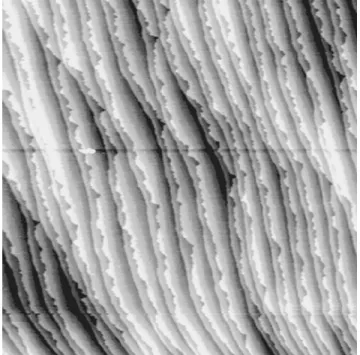
A clean Si~100! surface is known to exhibit a 231 recon-struction. Surface atoms form dimer rows to lower the sur-face energy by eliminating one of their two dangling bonds. Figure 1 depicts a 30 000330 000-Å2 STM image of the initially clean Si~100!-(231) surface. At this scale, indi-vidual atoms and dimers cannot be seen and the main feature are monoatomic steps. This image confirms the earlier find-ing concernfind-ing the Si~100!-(231) step structure.18The steps are alternatively smoother and rougher; they correspond to the so-called SA and SB steps, respectively. Each step
sepa-rates two degenerate reconstruction domains@231 and 132 domains# with dimer rows perpendicular to each other. The
231 @132# domains are the terraces with their dimer rows
running perpendicular~parallel! to the domain edges. Exposing clean Si~100!-(231) to digermane at room temperature results in randomly distributed dissociated frag-ments on the surface, which exhibits no correlation between Ge2H6 adsorption and local defects or steps. Figure 2~a!
indicates that the fully saturated surface with 15-L diger-mane was highly disordered. The digerdiger-mane-saturated ad-layer comprises a mixture of GeH2, GeH, SiH, and some
residual GeH3, and multiple internal reflection infrared
spec-troscopy and photoemission studies revealed.4,7 A previous ultraviolet photoemission spectroscopy study indicated that the exposure of digermane of Si~100!-(231) resulted in mo-lecular adsorption below 100 K, but generated a surface cov-ered with GeH3 radicals, stable between 110 and 150 K.
5
Hence, at room temperature, most GeH3 radicals further
de-compose to GeH2~ad! and H~ad!, which process breaks a
dimer bond by inserting H and leaves a saturated GeH2
radi-cal in a 131 surface site. Therefore, the disordered digermane-saturated surface displayed in Fig. 2~a! indicates that the GeH2 fragments on the surface are not sufficiently
mobile to form islands or clusters.
FIG. 1. STM image of a clean Si~100!-(231) surface. The scan range is 30 000330 000 Å2.
Subsequent heating of the digermane-saturated Si~100! surface has the effect of thermally decomposing the surface hydrides~GeH2 and GeH3) into GeH, liberating all the
ad-sorbed hydrogen and leaving only Ge atoms on the surface. This picture of thermal dissociation processes corresponds to the temperature-programmed desorption of H2
measure-ments, which comprises two H2 desorption maxima
a(;600 K! andb1(;800 K!.
5
The two desorption statesa andb1 attributed to H2 desorption from the decomposition
of GeH and SiH, respectively. Figure 2~b! displays a
4503450-Å2 STM image after annealing at 725 K for the
room-temperature saturated surface. The surface in Fig. 2~b! still lacked long-range ordering; however, the majority of the surface admolecules in the filled-state image ordered in lines
consisting of a few bright spots. These short linear trains lie in parallel on the same terrace and perpendicular to those on the terrace separated by a single atomic step. Furthermore, the direction of the trains are normal to the smoother SA
atomic steps, which are parallel to the dimer rows. The an-nealing temperature~725 K! was located between thea~600
K! and b1 ~800 K! desorption peaks in the H2
thermal-programmed desorption spectra. Therefore, it could be ex-pected that all the H attached to Ge had been driven off, and only Ge atoms and SiH species remained present on the sur-face. This reaction step was also confirmed by a previous photoemission study.7 In addition, the atomic chains in Fig.
2~b! appear to closely resemble the ‘‘diluted dimers’’
ob-served as the prevalent adsorbate configuration during the FIG. 2. STM images of~a! Si~100!-(231) saturated with a 15-L digermane dose at 300 K, and the same surface after annealing to ~b! 725,~c! 810 and, ~d! 900 K. The scanned areas are 4503450 Å2for~a!–~c!, and 100031000 Å2for~d!. The sample bias used with 22 V
for~a! and ~b!, and 12 V for ~c! and ~d!. A monoatomic step can be discerned around the lower left corner in ~a! and middle left corner in
MBE Si deposition at ;385 K.19 The ‘‘diluted dimers’’ are metastable lines of dimers arranged end to end. Each of the constituent dimers ordered in a line lie in a trough between substrate dimer rows and are perpendicular to them. All the above observations lead to attributing the linear chains in Fig. 2~b! to be Ge ‘‘diluted dimers’’ interspersed on the re-maining hydrogen terminated Si substrate. At this tempera-ture, Ge ad-dimers obtained from MBE posses sufficient dif-fusion energy to form large-two dimensional~2D! islands on clean Si~100!-(231). The formation of diluted dimers with partial ordering can be attributed to the hindrance of the Ge surface diffusion rate due to the presence of SiH.
Annealing a surface, such as that in Figs. 2~a! or 2~b! to 810 K for 60 s, resulted in the well-ordered surface depicted in Fig. 2~c!. The randomly dispersed digermane fragments in Fig. 2~a! were ordered to form 2D, buckled 231 islands. The dimer rows, which comprised the islands in Fig. 2~c!, are orthogonal to those of the substrate, and are consistent with the formation of a layer of a diamond structure. The substrate dimer rows also exhibited irregular buckling, which might be related to long-range interactions involving the 2D islands and their surroundings. Since the desorption maxi-mum of H2from SiH is about 800 K, annealing at 810 K for
60 s is sufficiently high to completely desorb hydrogen at-oms from the surface. Therefore, the 2D islands in Fig. 2~c! may be readily attributed to Ge dimers.
On the basis of Fig. 2~c!, the saturation coverage of di-germane of Si~100! can be estimated at rough 0.37 ML. To obtain a more precise picture of island coverage, Fig. 3 gives an overview image of a scale 300033000 Å2 for the same surface area depicted in Fig. 2~c!. Notably the islands in Fig. 3 dispersed uniformly on all the terraces, and the 2D islands did not exhibit much anistropy. From Fig. 3, the island cov-erage may be deduced to be 0.41. Since the Ge atoms incor-porated into the step edge cannot be taken into account, this coverage represents a lower bound. Furthermore, the dimer-ized 2D islands may represent only ;75% of the deposited
Ge while, at this temperature, the other ;25% move to the second layer, as indicated by the Ge 3d spectra in Fig. 4~b!
~see Sec. III B!. The saturation coverage may be estimated
nominally as 0.5 ML. which correlates closely with previous experimental results for Si2H6 adsorption on Si~100! and
Ge~100!.1,3,8Monte Carlo simulations also revealed that the
coverage for Si2H6 adsorption on Si~100! was limited to
0.43 ML, based on the similar surface reaction mechanism,3 on site blocking by H, and on steric hindrance. These find-ings together with a previous core-level photoemission study of thermal reactions indicates that the overall trends of ad-sorption mechanism for Ge2H6 closely resemble those for
Si2H6 interaction on Si~100!.8
Figure 2~d! depicts a well-ordered and relatively smooth surface after further annealing at 900 K. The 2D Ge islands appearing in Fig. 2~c! disappeared entirely. In Fig. 2~d!, three terraces separated by two monoatomic steps are observed. Within the domains, many short dark dimer vacancy lines
~VL’s! are clearly observable. Figure 2~d! indicates that
these VL’s are all perpendicular to the surround dimer rows and well separated, revealing the strong repulsion between VL’s. Although the length of the VL’s varies, they are uni-formly distributed on the entire surface. If the usual picture of step-flow growth occurred during annealing, the 2D Ge islands in Fig. 3 should simply diffuse and adhere to nearby steps. Once Ge atoms are incorporated into the original steps, remaining intact, the immediate formation of a well-defined
23n structure @see Fig. 6~a!# in those areas coexists with the
remaining clean Si-terminated 231 areas. However, the STM image does not reveal any supposed contrast between the Ge-terminated regions and the original, Si-terminated ar-eas, and none was observed on the surfaces of a similar growth system by low-energy electron diffraction and mi-croscopy either.12 It is thus clear, as proposed by Tromp,12 that Ge atoms displace Si in the terrace and together form a relatively homogeneous, mixed Ge-Ge and Si-Si dimer sur-face. It is also notable that all the surface dimers in Fig. 2~d! appeared buckled. By comparison, at room temperature, only certain portions of the dimers on the clean Si~100!-(231) were asymmetric.
B. Multilayer growth by atomic-layer epitaxy
As noted above, saturating the Si~100! surface with diger-mane at room temperature followed by high-temperature an-nealing yielded a net deposition of around 12 ML of Ge.
Re-peating the cycle results in a controllable, quantized deposition generally known as atomic-layer epitaxy. In this study, an initial saturation exposure of 15 L and an annealing temperature of 900 K for 60 s where selected. Although Ge deposition at this annealing temperature produces films that are not in their thermodynamical ground state,17the tempera-ture is sufficiently high to promote step flow and island in-corporation for smooth film growth, as is depicted in Fig.
2~d!, while minimizing the possible intermixing between Si
and Ge.
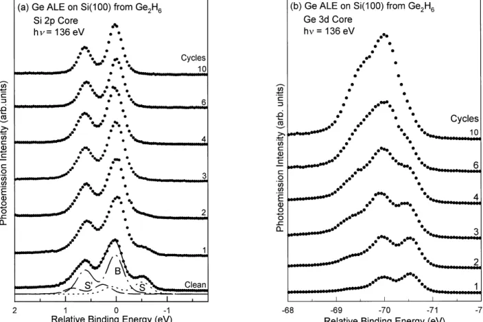
Figures 4~a! and 4~b! display photoemission spectra of Si 2 p and Ge 3d, respectively, for various numbers of cycles of Ge deposition. The binding energy refers to the bulk compo-nent of the Si 2 p3/2line~see below!. The bottom spectrum of
Fig. 4~a! represents a surface-sensitive Si 2p spectrum for FIG. 3. Large area STM image for the same surface of Fig. 2~c!.
The area is 300033000 Å2.
clean Si~100!-(231) and the results of a least-squares analy-sis. Following standard procedure, the spectrum is analyzed in terms of three spin-orbit-split components S, S
8
, and B of identical line shape, corresponding to signals derived from the dimerized surface layer, the second layer, and the bulk, respectively.20The S component is responsible for the well-separated shoulder on the lower-binding-energy side, and its intensity can be deduced by fitting. Upon deposition of Ge by ALE from Ge2H6, the intensity of S decreases nearly tozero after two growth cycles, indicating that the surface be-comes a Ge layer and the top layer of Si then bebe-comes a second layer. The presence of S
8
in the Si 2 p spectrum for the clean Si~100! is shown by the valley between two spin-orbit-split peaks of the B component filling in. The S8
com-ponent began decreasing slowly and completely disappeared after more than six cycles of Ge growth. The reduction of the S8
component can be best understood by examining the changes in the relative depth of the valley between the two spin-orbit peaks. At ten cycles (;5 ML coverage! of Ge growth, the line shape of the top spectrum in Fig. 4~a! con-sists of only two spin-orbit peaks, reflecting the bulk emis-sion. This is because the bonding between Si and Ge closely resembles that of Si and Si, and, as a result, all Si atoms under such a thick layer of Ge are in a bulklike bonding environment.The line shapes of the Ge 3d for the bottom three spectra in Fig. 4~b! can be decomposed into a few components. The FIG. 4. Photoemission spectra ~filled circles! for ~a! the Si 2p and ~b! and Ge 3d core levels for various numbers of cycles of ALE growth of GE on Si~100!. Each cycle involves an exposure of 15-L digermane at ;325 K followed by annealing at 900 K. The bottom spectrum of~a! is for the clean Si~100!-(231) surface. The solid curve is a fit to the spectrum. The curves labeled B, S, and S8are the results of a decomposition into individual components which consist of a pair of spin-orbit split peak. The B component is derived from the bulk; S and S8are surface related. The relative binding energy refers to the Si 2 p3/2line of the B component.
FIG. 5. Integrated photoemission intensity ~circles! and photo-emission intensity of the S component alone~filled squares! of Ge 3d for various cycles of Ge growth on Si~100!. Each cycle involves an exposure of 15-L digermane at;325 K followed by annealing at 900 K.
implications are discussed in Sec. III C. The broadening and loss of characteristic features in Ge 3d line shapes for six and ten cycles can be attributed to the gradually increasing surface roughness and disorder. The integrated intensity of Ge 3d as a function of growth cycles is plotted in Fig. 5. The net Ge deposition in each cycle is expected to be about the same due to the chemical similarity of Ge and Si dimers. However, the indiffusion of partial Ge population into deeper layers ~see Sec. III C! reduce the integrated intensity of Ge 3d due to a short electron mean free path, leading to slight deviation of the data points in Fig. 5 from a linear incline. The overall trends of these Si 2 p and Ge 3d spectra in Figs.
4~a! and 4~b! closely correlate with those found during MBE
growth of Ge, and the calibration of the Ge coverages should be more satisfactory here since ALE was employed.
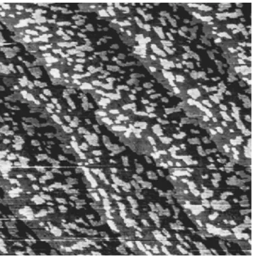
Figures 6~a!, 6~b!, 6~c!, and 6~d! depict the surface after
two, six, nine, and 15 cycles of Ge growth of Si~100!, re-spectively. In Fig. 6~a!, the 23n ~on an average, n;12) reconstruction, signaled by the dark VL’s, is clearly observ-able. The VL’s extend for hundreds of Å but the ordering of the 23n structure is poor in that the distance between two VL’s exhibits a very broad distribution. As the Ge coverage increases to ;3 ML, the VL’s concentration also increases, as Fig. 6~b! illustrates. This figure basically depicts the same
23n reconstruction as Fig. 6~a!, but the VL’s concentration
increases~on an average, n;8) and the degree of 23n or-dering appears better in that the distribution of n is sharper. These observations were fairly consistent with previous STM studies of Ge-covered Si~100! utilizing MBE for correspond-ing coverages.18 The formation of a 23n structure and its degree of ordering has been associated with stress changes on the Ge-covered Si~100!. Since there are no trenches in the FIG. 6. 100031000-Å2STM images of Si~100! after ~a! two, ~b! six, ~c! nine, and ~d! 15 cycles of ALE growth of Ge. Each cycle involves an exposure of 15-L digermane at;325 K followed by annealing at 900 K.
second layer at the locations of the VL’s of the first layer in Fig. 6~b!, the dimer vacancies must have been filled. Upon completing nine cycles (;4.5 ML! of Ge ALE growth, multilayer growth had started, as Fig. 6~c! indicates. Aug-menting ALE growth cycles results in increased surface roughness, as illustrated in Fig. 6~d!. Figure 6~d! basically depicts a multilayer surface, each layer consisting of many small 23n domains bounded by VL’s of the same layer and trenches, which are extensions of those VL’s on deeper lay-ers. These measurements were consistent with previous re-ports which confirmed that the Ge growth on Si~100! is layer by layer, up to a thickness of;3 ML with the surface main-taining a nominal 231 structure.13–16
C. Chemical composition of the dimer layer
In the above sections, interpreting the data was based on a theoretical calculation which revealed that Ge possesses a lower surface energy, and that a full layer of Ge covers the surface of a Ge0.5Si0.5~100! alloy.21 Full Ge termination upon the adsorption of Ge on Si~100! at 1 ML or above of coverage was also clearly suggested both by theoretical calculations17 and many experimental studies employing low-energy electron microscopy,12 low-energy electron diffraction,13, STM,13–15and ultrahigh vacuum transmission microscopy.16 As Ge is deposited on Si~100!, however, a surface layer consisting of a mixture of Si-Ge dimers is speculated to form beneath a 1-ML coverage.22 Distinguish-ing between Si-Si, Ge-Ge, and Si-Ge dimers is a problem, because Si and Ge are extremely similar to their atomic, electronic, and chemical properties. Therefore, the atomistic process of Ge incorporation and the compositional distribu-tion of the surface and subsurface regions all remain unclear, despite extensive studies.
These questions concerning the initial stages of growth are also attended by problematic interpretations of the atomic origins of surface-shifted core levels in the photoemission spectra for the clean Si~100!-(231) and Ge on Si~100! (231).20,22–26 In Sec. III B, the peak assignment for the S components in the Si 2 p spectrum for clean Si~100! in Fig.
4~a! is one complete monolayer of dimerized Si atoms on the
surface, including both up and down dimer atoms in the asymmetric dimer model. An alternative interpretation is to attribute the S component to up dimer atoms only ~one-half of a monolayer!. These differing interpretations may be ferred to as the full-layer and half-layer interpretations, re-spectively. In two previous photoemission studies of MBE growth of Ge on Si~100!, similar results for Si 2p and Ge 3d core-level spectra were variously attributed to the different thicknesses of calibration of film growth in the submono-layer region.20,22For example, the intensity of the S compo-nent, which is a quantitative measure of the surface area that remains clean, decreased to zero at;0.5 ML in Ref. 22 but
at;1 ML in Ref. 20. The authors of Ref. 22 thus concluded
that Ge initially grows as asymmetrically mixed Ge-Si dimers, with Ge occupying the up atoms since their emission from the up Si atoms ~the S component! disappears at a 0.5-ML coverage. On the other hand, the authors of Ref. 20 referred to the 1-ML interpretation, based on assuming pure Ge-Ge dimer growth for the first monolayer, and on the fact that the S component is eliminated at a ;1-ML Ge
cover-age. As indicated in Sec. III B, the atomic-layer epitaxial growth of Ge from Ge2H6 offers quantized deposition and,
therefore, should provide a self-calibrated thickness mea-surement. In Fig. 4~a!, the intensity ratio of S/B decreased
;70% from 0.275 for clean Si~100!-(231) to ;0.09 for
one cycle of growth and ;95% for two cycles. Assuming that the saturation coverage of 0.5 ML is accurate, the cov-erage determinations in Ref. 20 are higher than, and those in Ref. 22 lower than, the actual values.
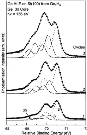
Figure 7 displays Ge 3d core-level spectra taken from Fig. 4~b! for the first three cycles of Ge growth and the results of decomposition. Note that the Ge 3d spectrum taken from clean Ge~100!-(231) in Ref. 8 shows a line shape closely resembling that of Si 2 p for Si~100!-(231) due to the similarity of the two surfaces. There are again three major components, B, S
8
, and S, where the S compo-nent, shifted to lower binding energies, can be associated with the dimers on the surface. For a more relevant compari-son with the spectra in Ref. 22, the line shapes in Fig. 7 are described as the combination of three components S, SS, and S8
accordingly. The authors of Ref. 22 assigned peaks S, SS, and S8
to the up atoms of mixed Ge-Si dimers, the down atoms of pure Ge-Ge dimers, and Ge in deeper layers, even though most theoretical and experimental studies have indi-cated that the interface between the grown Ge film andSi~100! substrate is abrupt.12–15,27 In an attempt to analyze
the absolute atomic population of the S component in Ge 3d spectra, the relative emission intensity of the S component FIG. 7. The decomposition of the Ge 3d spectra @taken from Fig. 4~b!# into three curves (S, SS, and S8) for the first three cycles of ALE growth of Ge on Si~100!. The solid curves are overall fit to the spectra. Details of the peak assignments are given in the text.
for the first four growth cycles was measured by monitoring the photocurrent from a gold mesh, the results of which pro-cedure are plotted in Fig. 5. After the first growth cycle, the intensity of the S component accounts for 70–80 % of the total Ge 3d emission~depending on using two or three com-ponents in the fitting!, or ;0.4-ML Ge atoms, assuming that the total amount of Ge is 0.5 ML. The S intensity increased by around 50%, 70%, and 70% after two, three, and four growth cycles, respectively. Attempting to deduce the inten-sity for higher growth cycles yielding values close to that of the fourth growth cycle. However, the uncertainty is consid-erable, since the line shapes are broad and do not easily afford satisfactory fits. The calculated population of the S component is, therefore,;0.65 ML at the end of four growth cycles. The number of dimer vacancies on the corresponding Ge-covered Si~100! surface is ;13%. Moreover, the core-level emission from the Ge dimers on two sides of the dimer vacancies can easily contribute to the S
8
or SS peaks due to the charge transfer upon rebonding the second-layer atoms underneath the dimer vacancies.28 These populations to-gether sum up to;1 ML. This finding is also consistent with theoretical studies which have revealed that the surface of Ge-covered Si~100! is terminated completely by Ge above 1-ML coverage.17 Because the energy associated with sur-face strain is only a fraction of an meV/atom,17 which is far smaller than the typical energies encountered in the kinetic processes, it is unlikely that the mixed Ge-Si dimers would become an energy ground state if and only if the Ge cover-age is less than 1 ML.If the 2D islands in Fig. 2~c! consist mainly of Ge-Si mixed dimers and thus incorporate only;0.2 ML of the Ge populations, the surrounding substrate areas must contain the rest of Ge ~0.2–0.3 ML! occupying the up atom positions. The scenario of the atomistic process of forming the surface of Fig. 2~c!, in such a case, is that about half of the Ge population displaces Si from the substrate to form Ge-Si dimers, and the expelled Si diffuse and form mixed Ge-Si islands with the other half of the Ge. If this picture describes the growth of the first cycles accurately, the atomic arrange-ments for Ge in Figs. 2~c! and 2~d! and their associated Si-Ge misfit strains are essentially the same, despite the dif-ferent morphology of the two surfaces, since the line shapes for Si 2 p and Ge 3d spectra remain largely unchanged at annealing temperatures above 810 K. However, no dimer vacancy lines such as those appearing in Fig. 2~d! can be observed in Fig. 2~c!.
The above considerations suggest that the pure Ge dimers are stable species during the deposition of Ge/Si~100!. The conclusion that Ge predominantly grows as mixed Ge-Si dimers up to 0.8 ML by Pattey et al. was solely drawn based on the thickness determinations, which could also be problematic.22 The deposition of 0.5-ML Si atoms on
Ge~100!-(231) using disilane is a very similar, although not
identical, system for comparison.8A previous photoemission study of this system showed that the intensity of the Si 2 p core level drops by more than 70% after the desorption of H. If the Si atoms merely moved into the down dimer positions, there would be little reduction, but the intensity reduction is too large for all these Si atoms to reside in the layer just below the dimer layer. Most of them must have moved into deeper layers, and the composition of the upper most atomic layer consists of nearly 100% Ge. This phenomena clearly indicates that the Ge-Ge dimers are energetically more favor-able than Ge-Si dimers. However, the surface composition of the Ge/Si~100! systems is not likely to be in the idealized states with 100% pure Ge-Ge dimers. Since the entropy fac-tor is important at a high temperature, randomly mixed states consisting of both Ge-Ge and Ge-Si dimers become more favored, as illustrated in Ref. 21.
IV. SUMMARY
Combining microscopy ~STM! and spectroscopy ~core-level photoemission! techniques provided detailed infoma-tion about the growth process and the consequent surface structure of Ge ALE on Si~100!-~231! employing diger-mane. At room temperature, the adlayer on Ge2H6
-saturated Si~100!-(231) appeared to be completely disor-dered. When the digermane-saturated surface was heated to 725 K for 1 min, the formation of partially ordered diluted Ge dimer chains was observed. The surface was interspersed with large 2D islands covering ;41% of its area. No de-nuded zone was present on the surface, in contrast to that during MBE. At 900 K, the surface-recovered 231 dimer rows interrupted by poorly ordered short dimer vacancy lines with no observable contrast on the atomic terraces. Multilayer Si deposition was performed by ALE, i.e., cyclic digermane adsorption at near room temperature followed by thermal annealing at 900 K. Overall, the trends observed for multilayer Ge deposition in the present ALE experiments were similar to those for MBE Ge thin-film growth. The chemical composition of the surface layer resulting from mixed Ge-Si or Ge-Ge forming during submonolayer adsorp-tion of Ge on Si~100! was discussed.
ACKNOWLEDGMENTS
The authors wish to thank the National Science Council, Republic of China in Taiwan, for financially supporting this work under Contract Nos. NSC86-2613-M009-001 and NSC85-2112-M009-024. The authors are also grateful to T.-W. Pi for loaning us the photoemission chamber, to T.-C. Chiang for discussions, and to P. Wagner of Wacker Sil-tronic for providing samples.
1D. Lubben, R. Tsu, T. R. Bramblett, and J. E. Greene, J. Vac. Sci.
Technol. A 9, 3003~1991!, and references therein.
2S. M. Gates, Surf. Sci. 195, 307~1988!; R. Imbihl, J. E. Demuth,
S. M. Gates, and B. A. Scott, Phys. Rev. B 39, 5222~1989!.
3J. J. Boland, Phys. Rev. B 44, 1383~1991!.
4B. M. Ning and J. E. Crowell, Appl. Phys. Lett. 60, 2914~1992!;
Surf. Sci. 295, 79~1993!.
5D.-A. Klug, W. Du, and C. M. Greenlief, J. Vac. Sci. Technol. A 11, 2067~1993!; Chem. Phys. Lett. 67, 2187 ~1991!.
6M. J. Bronikowski, Y.-W. Wang, M. T. McEllistrem, D. Chen,
and R. J. Hamers, Surf. Sci. 298, 50~1993!.
7D.-S. Lin, K.-H. Huang, T.-W. Pi, and R.-T. Wu, Phys. Rev. B 54, 16 958~1996!.
8
D.-S. Lin, T. Miller, and T.-C. Chiang, Phys. Rev. B 47, 6543
~1993!.
9J. M. Heitzinger, J. M. White, and J. G. Ekerdt, Surf. Sci. 299,
892~1994!, and references therein.
10H. Temkin, J. C. Bean, T. P. Pearsall, N. A. Olson, and D. V.
Lang, Appl. Phys. Lett. 46, 155~1986!.
11R. A. Soreff, Proc. IEEE 81, 1687~1993!.
12R. A. Tromp and M. C. Reuter, Phys. Rev. Lett. 68, 954~1992!;
R. A. Tromp, Phys. Rev. B 47, 7125~1993!.
13U. Ko¨kler, O. Juska, B. Mu¨ller, M. Horn-von Hoegen, and M.
Pook, Ultramicroscopy 42-44, 832~1992!; F. Iwawaki, M. To-mitori, and O. Nishikawa, ibid. 42-44, 902~1992!.
14Y.-M. Mo and M. G. Lagally, J. Cryst. Growth 11, 876~1991!. 15T. Nakayami, Y. Tanishiro, and K. Takayanagi, Surf. Sci. 273, 9
~1992!.
16M. Hammer, F. K. Legoues, J. Tersoff, M. C. Reuter, and R. M.
Tromp, Surf. Sci. 349, 129~1996!.
17F. Liu and M. G. Lagally, Phys. Rev. Lett. 76, 3156~1996!, and
references therein.
18F. Wu, X. Chen, Z. Zhang, and M. G. Lagally, Phys. Rev. Lett. 74, 564~1995!, and references therein.
19P. J. Bedrossian, Phys. Rev. Lett. 74, 3648~1995!; A. van Dam,
J. van Wingerden, M. J. Haye, P. M. L. O. Scholte, and F. Tuinstra, Phys. Rev. B 54, 1557~1996!.
20D.-S. Lin, T. Miller, and T. C. Chiang, Phys. Rev. Lett. 67, 2187
~1991!.
21P. C. Kelires and J. Tersoff, Phys. Rev. B 63, 1164~1989!. 22L. Pattey, E. L. Bullock, T. Abukawa, S. Kono, and L. S. O.
Johansson, Phys. Rev. Lett. 75, 2538~1995!.
23E. Landemark, C. J. Karlsson, Y.-C. Chou, and R. I. G. Uhrberg,
Phys. Rev. Lett. 69, 1588~1992!.
24J. E. Rowe and G. K. Wertheim, Phys. Rev. Lett. 69, 550~1992!;
F. L. Himpsel, ibid. 69, 551~1992!; D.-S. Lin, J. A. Carlisle, T. Miller, and T. C. Chiang, ibid. 69, 552~1992!.
25X. Yang, R. Cao, J. Terry, and P. Pianetta, Phys. Rev. B 45, 13
749~1992!.
26
J. H. Cho, S. Jeong, and M. H. Kang, Phys. Rev. B 50, 17 139
~1994!.
27D. E. Jesson, S. J. Pennycook, and J.-M. Baribeau, Phys. Rev.
Lett. 66, 750~1991!.