ORIGINAL ARTICLE
Extremely anisotropic single-crystal growth
in nanotwinned copper
Chia-Ling Lu
1, Han-Wen Lin
1, Chien-Min Liu
1, Yi-Sa Huang
1, Tien-Lin Lu
1, Tao-Chi Liu
1,
Hsiang-Yao Hsiao
1, Chih Chen
1, Jui-Chao Kuo
2and King-Ning Tu
3By electroplating of nearly unidirectionallyo1114-oriented nanotwinned and fine-grained Cu on a Si wafer surface followed by annealing at 400–500 °C for up to 1 h, we grew many extremely large o1004-oriented single crystals of Cu with sizes ranging from 200 to 400μm. By patterning and annealing the nanotwinned Cu films, we grew an array of o1004-oriented single crystals of Cu with sizes ranging from 25 to 100μm on Si. In comparison, single-crystal nano-wire growth is a one-dimensional anisotropic growth process, in which the growth along the axial direction is much faster than in the radial direction. We report here a bulk-type two-dimensional crystal growth of an array of numerouso1004-oriented single crystals of Cu on Si. This growth process has the potential for microbump applications in three-dimensional integrated circuit-packaging technology for hand-held consumer electronic products.
NPG Asia Materials (2014) 6, e135; doi:10.1038/am.2014.90; published online 3 October 2014
INTRODUCTION
With the popularity of hand-held devices, mobile consumer electronic products are expected to undergo a very rapid growth in the global semiconductor market in the near future. As Si chip technology approaches the limit of Moore’s law, the microelectronic industry is turning to packaging technology to extend the limit using three-dimensional integrated circuits (3D ICs), which, in essence, represents the merging of chip technology and packaging technology. On a limited chip area and in a tight device space, the best way to increase the density of high-performance transistor circuits is to stack the chips vertically, that is, in 3D ICs.
For a successful merger, precise fabrication of the microstructure in the packaging technology is required. In the trend of miniaturization of Si chip technology, the precise fabrication of hundreds of millions of transistors and their gates and contacts on a Si chip has been the foundation of Moore’s law. One example is the use of lattice strain to increase the carrier mobility in Si channels. In 3D ICs, there are thousands of microbumps on a through-Si-via chip, and precise control of the microstructure of all the microbumps is required, which is a new paradigm in the microelectronic industry. Because the merging of chip technology and packaging technology is needed to extend Moore’s law, it is crucial to have precise control of manu-facturing in packaging technology.
We consider the diameter of a solder joint below. In flip chip packaging technology, the diameter is ~ 100μm, and in microbumps for 3D IC packaging, the diameter is ~ 10μm. When the diameter changes by 10 times, the volume changes by 1000 times, which indicates that if we assume that the grain size is 10μm, the
microbump will consist of one grain; however, theflip chip joint will contain 1000 grains. Clearly, we can assume an isotropic microstruc-ture in the latter, and microstrucmicrostruc-ture control is not a concern; however, in the former, the microstructure is anisotropic, for example, the orientation of a grain can change from one microbump to another microbump. The anisotropy tends to cause early failure of micro-bumps in the high-performance devices; thus, precise microstructure control is required.
Microstructure control starts from crystal growth, which is one of the most important topics in multi-disciplinary sciences because the crystal growth controls the properties of semiconductors, metals and ceramics in thermal processing.1–11 Crystal growth from a melt is known to be anisotropic, which is evidenced by facet formation. In the solid state, crystal growth is manifested by grain growth, which tends to be isotropic, especially in centered cubic metals. Many faced-centered cubic metal thinfilms exhibit abnormal grain growth after annealing. Several researchers have reported that giant grains up to several hundred micrometers can be grown in Al,12,13Ag14,15and Cu
thinfilms.16,17However, we report here a new type of abnormal grain
growth that results from the extremely anisotropic two-dimensional crystal growth of Cu via nearly unidirectionally oriented nano-twins; the growth in the vertical direction is much slower than that in the lateral directions. In comparison, single-crystal nano-wire growth is a one-dimensional anisotropic growth process in which the growth along the axial direction is much faster than that along the radial direction. Although graphene is grown using two-dimensional aniso-tropic growth, this process involves single atomic layer growth and hardly any growth in the vertical direction. We applied the extremely
1Department of Materials Science & Engineering, National Chiao Tung University, Hsinchu, Taiwan, Republic of China;2Department of Materials Science & Engineering, National
Cheng Kung University, Tainan, Taiwan, Republic of China and3Department of Materials Science and Engineering, University of California at Los Angeles, Los Angeles, CA, USA
Correspondence: Professor C Chen, Department of Materials Science & Engineering, National Chiao Tung University, Hsinchu, Taiwan 30010, Republic of China. E-mail: [email protected]
anisotropic growth to grow an array of numerous (100) single-crystal microbumps of Cu on a Si surface.
Exceptionally large grain growth in polycrystalline Cu is known as abnormal grain growth, in which a bimodal distribution of the grain size is obtained.5The larger grains are the abnormal grains. We note
that in our extremely anisotropic growth, we do not have a bimodal distribution; instead, we have a normal grain size distribution of all the {100} grains. When we patterned theo1004-oriented single crystals of Cu on a Si wafer surface, the grain size exhibited a mono-size distribution. The size was the diameter of the Cu microbump, which varied from 25 to 100μm. This mode of crystal growth is unique, in which numerous single crystals of the same size are grown at the same time. For the typical mode of abnormal grain growth, it would not be possible to obtain the {100} single crystals from those small grains in the bimodal distribution.
MATERIALS AND METHODS
Highly oriented o1114 Cu grains with densely packed nanotwins were fabricated by pulsed electroplating. A high-purity CuSO4solution was adopted
as the electrolyte, and a high-purity 99.99% copper sheet was employed as the cathode. Proper surfactants and 40 p.p.m. HCl were added to the electrolyte. A Si wafer was adopted as the substrate, and a TiW layer with a thickness of 200 nm was sputtered as the adhesion layer, followed by sputtering of a 200-nm-thick o1114 Cu as a seed layer using an Oerlikon ClusterLine 300 machine (OC Oerlikon Corporation AG, Pfäffikon, Switzerland). The Si wafer was cut into pieces of 3 × 1 cm2or 2 × 1 cm2, and these pieces were immersed
in the electrolyte during pulsed electroplating. The stirring rate to grow the oriented nanotwinned Cu (nt-Cu) was 600 r.p.m., and the current density was 50 mA cm− 2. The duty cycles wereTon= 0.02 s and Toff= 1.5 s. The deposition
rate was 1.2 nm s− 1under this electroplating condition. Thefilm thickness was controlled to be ~ 8μm in this study. For the preparation of the equivalent Cu layer without the nanotwins, we used the same electroplating solution at 200 mA cm− 2.
To investigate the grain growth of Cu, the Cu films were subjected to annealing at temperatures ranging from 400 to 500 °C for extended periods. A
quartz-tube furnace with a vacuum at 5 × 10− 7torr was used for the annealing. After annealing, a focused ion beam (FIB) was employed to examine the grain structure of the Cufilms. X-ray diffraction was used to analyze the preferred texture of the Cu films. Electron backscattered diffraction (EBSD) was performed to examine the individual grain orientation in the Cufilms. The EBSD measurements were performed with a JEOL 7001 F field-emission scanning electron microscope (JEOL Ltd., Tokyo, Japan) with an EDAX/TSL system operated at 25 kV. The analysis was performed with a step size of 50 nm for the Cu grains. OIM software (TSL, Inc., Draper, UT, USA) was used to analyze the crystallographic orientation maps and preferred orientations based on Kikuchi patterns.
RESULTS AND DISCUSSION
We begin with the results of electroplatingo1114-oriented, nt-Cu on Si wafers. The spacing of the nanotwins ranged from 10 nm to 100 nm.18Highly orientedo1114 nt-Cu was fabricated on the seed layer.
Figures 1a and b show the plan-view of the inverse polefigure map from EBSD and the preferred orientation for the inverse polefigure on the surface grains fabricated at 50 mA cm− 2, respectively. The surface grains are all o1114 oriented, and the average grain size for this condition is 2.38± 0.85 μm. X-ray diffraction also reveals that the Cu film possesses an extremely high o1114 texture, as illustrated in Figure 1c. Figure 1d plots the statistical data for the misalignment angles of the Cu (111) grains in Figure 1a. The misorientation angle of a grain is defined as the angle difference between the pole of the grain and the normal direction to the Si substrate. The average misorienta-tion was obtained by averaging the misorientamisorienta-tion angles for all the grains in the EBSD image. For the as-fabricated o1114-oriented grains in Figure 1a, the average misorientation was 6.4°. An FIB top view of the nt-Cu microstructure is provided in Supplementary Figure S1a in Supplementary Information. All of the {111} twin planes are parallel to the wafer surface; thus, their normal, theo1114 axis, is perpendicular to the wafer surface. EBSD indicates that nearly all of the grains are o1114 oriented; we observe a very high degree of
Figure 1 Preferred orientation of the as-deposited Cufilm. (a) Plan-view of the inverse pole figure map from for the o1114-oriented surface grains with color coding of the inverse polefigure. (b) The inverse pole figure of the fabricated Cu film in terms of the out-of-plane direction in a. (c) X-ray diffraction for the as-deposited Cufilm. (d) The statistical results showing the numerical fraction of grains as a function of the misalignment angle from the [111] direction.
o1114 texture, over 90%, compared with the value for most published studies on textured Cufilms of ~ 20%.19By annealing the
oriented nt-Cu in the temperature range of 400–500 °C for a few minutes, we obtained some exceptionally large grains that had diameters of ~ 200–400 μm. A top view of one of these grains is presented in Figure 2a; this grain is ~ 65 times larger than the surrounding grains and appears as an abnormal grain. The inverse polefigure map for the grains reveals that the large grain is o1004 oriented. The corresponding FIB image for the grains is presented in Supplementary Figure S1b. Figure 2b shows an enlargement of the white rectangle area in Figure 2a. Figure 2c illustrates the evolution of the X-ray diffraction spectra of a sample annealed at 450 °C for various times, and we observed only two peaks of {111} and {200} diffraction; the intensity of the latter increases, whereas the former decreases with annealing time.
To convert the abnormal grain growth to solid-state crystal growth, we patterned an array of nt-Cu bumps with diameters ranging from 100 to 25μm and thicknesses of 10 μm using a lithographic technique. Figure 3a presents the EBSD inverse polefigure map for a 100-μm-diameter circular bump ofo1114-oriented nt-Cu in the as-plated state. The grains are allo1114 oriented. Supplementary Figure S2a presents a corresponding plan-view FIB image of the bump. After annealing at 450 °C for 60 min, Figure 3b presents an image of nine bumps; six of these bumps were completely transformed into a o1004-oriented single-crystal of Cu, and the other three were very near complete transformation. The corresponding plan-view FIB
image is presented in Supplementary Figure S2b. To verify whether the entire bump was transformed into a single crystal, one of the o1004 bumps was etched by FIB. Figure 3c presents the tilted view of the bump, and the entire bump is a single crystal. We were also able to produce an array ofo1004 Cu single crystals with diameters of 75, 50 and 25μm, as shown in Figure 4. This figure demonstrates the precise control of growth of an array of single-crystal Cu microbumps. The blurry edges in Figure 4f may be attributed to the electron-charging effect in the scanning electron microscope. The 75-μm Cu pads in Figure 4d occupy ~ 55% of the surface area. However, the 25-μm Cu pads in Figure 4f occupy only ~ 8% of the surface area. Therefore, the electron-charging effect may occur in the sample with 25-μm Cu pads.
Furthermore, when molten Pb-free solder reacts with a o1004-oriented single-crystal Cu, an o1004-oriented growth of the intermetallic compound of Cu–Sn was obtained.20In the microbumps for 3D IC
interconnects, the amount of solder is very small. Thus, the properties of the Cu–Sn intermetallic compounds, not the solder, will dominate the performance of the microbumps. When a few microns of solder were used, all of the solder transformed to Cu–Sn intermetallic compounds after reflow.21,22Therefore, theo1004-oriented
single-crystal Cu pads can be used to control the electrical and mechanical properties of the microbumps because the growth of oriented intermetallic compound can be controlled.
To determine the mechanism of anisotropic grain growth, we examined cross-sectional views in Figure 5 of samples before
Figure 2 Two-dimensional anisotropic crystal growth ino1114 nt-Cu films. (a) Plan-view inverse pole figure map of the large o1004 grain obtained from electron backscattered diffraction. (b) Enlarged inverse polefigure map for the dashed rectangle in a. (c) Evolution of the X-ray diffraction intensities for the samples annealed at 450 °C for various times.
Figure 3 Fabrication ofo1004 Cu single crystals after annealing at 450 °C for 60 min. (a) Plan-view electron backscattered diffraction inverse pole figure map for the as-fabricatedo1114 Cu crystals. (b) The inverse pole figure map labeled with the crystal lattice for nine o1004 single crystals. (c) Focused ion beam tilt image showing the etched cross-section for ao1004 single crystal.
(Figure 5a) and after (Figures 5b and c) annealing at 400 °C for 20 min. Theo1004 grain on the left-hand side of Figures 5b and c grew laterally to 290μm. However, its height was only ~ 5 μm in the vertical direction. The anisotropic grain growth has a very slow growth
in the vertical direction, which is at least 50 times slower than the lateral growth. In the o1004-oriented grains, no nanotwins are detected. Furthermore, the anisotropic grain growth started from the bottom interface rather than from the free surface.
Figure 4 Fabrication of arrays ofo1004 Cu single crystals. Plan-view electron backscattered diffraction inverse pole figure map for as-fabricated o1114 Cu crystals: (a) 75-μm diameter, (b) 50-μm diameter and (c) 25-μm diameter. After annealing at 450 °C for 60 min, the o1114 Cu crystals transformed intoo1004 single crystals: (d) 75-μm diameter, (e) 50-μm diameter and (f) 25-μm diameter.
Figure 5 Extremely anisotropic growth of theo1004 Cu crystals. (a) sectional focused ion beam (FIB) image of the as-fabricated sample. (b) Cross-sectional inverse polefigure map of the large o1004 crystal with a lateral crystal size of 290 μm. (c) Cross-sectional FIB image of the sample in b. (d) Plan-view of the inverse polefigure map from electron backscattered diffraction for the sample annealed at 450 °C for 25 min. (e) Grain size distribution for the grains in d.
In Figure 5, when we carefully examine the interface at the bottom between the substrate and the columnar nanotwinned grains, we observe a very thin seeding layer of Cu with a high density of o1114-oriented tiny grains of Cu; however, some randomly oriented
tiny grains of Cu are also observed, including a few of the o1004-oriented grains, which serve as nuclei of the growth of the anisotropic large grains. The very thin seeding layer was deposited to enhance the growth of theo1114-oriented nt-Cu layer during electroplating. The
Figure 6 Texture of the 200-nm-thick Cu seed on the TiW adhesion layer. (a) Plan-view of the inverse polefigure map for the o1114- and o1004-oriented seed layers with color coding of the inverse polefigure. (b) The inverse pole figure of the Cu seed layer in terms of the out-of-plane direction in a. (c) X-ray diffraction for the Cu seed layer.
Figure 7 Orientation evolution in the nt-Cufilms after annealing at various temperatures. (a) X-ray diffraction of nt-Cu films annealed at temperatures ranging from 300 to 500 °C for 30 min. (b) A plot of the {111} and {200} intensities versus annealing temperature. Theo1004 preferred orientation increases as the annealing temperature increases.
Figure 8 Extremely anisotropic growth of theo1004 Cu grains. (a) Cross-sectional map of the inverse pole figure from electron backscattered diffraction (EBSD) for the sample annealed at 350 °C for 30 min. (b) The corresponding cross-sectional focused ion beam (FIB) image for the sample in a. (c) Cross-sectional map of the inverse polefigure from EBSD for the sample annealed at 400 °C for 10 min. (d) The corresponding cross-sectional FIB image for the sample in c. (e) Cross-sectional FIB images for the sample after annealing at 400 °C for 20 min.
microstructure of the seeding layer is shown in Figure 6. The Cu seed layer has a crucial role in the extremely anisotropic single-crystal growth. Figures 6a and b present the plan-view of the inverse pole figure map from EBSD and the inverse pole figure of the out-of-plane direction, respectively, for the Cu seed layer sputtered on the TiW adhesion layer. The Cu seedfilm is highly o1114 oriented. However, it is noteworthy that some of the grains wereo1004 oriented, as indicated by the inverse polefigure in Figure 6b. Figure 6c shows the X-ray reflections for the Cu seed layer. The diffraction also indicates that the seed layer possesses a strongo1114 texture. However, the intensity of the Cu {200} and {220} reflections was still detectible. These pre-existingo1004 seed grains will act as nucleation sites for extremely anisotropic grain growth of Cu.
To confirm that the anisotropic single-crystal growth started from the substrate interface, we performed a systematic investigation of the transformation of the o1114-oriented nt-Cu into the o1004 anisotropic grains between 300 and 500 °C for 30 min. Figure 7 shows the evolution of the X-ray diffraction spectra for the Cufilms annealed at 300, 350, 400, 450 and 500 °C for 30 min. Figure 7a presents the
X-ray diffraction spectra of the nt-Cufilms annealed at 300, 350, 400, 450 and 500 °C for 30 min. Figure 7b plots the intensity of the Cu {111} and {200} reflections in Figure 7a. The intensity of the {111} reflection decreases as the temperature increases. However, the intensity of the {200} reflection increases as the temperature increases. Transformation ofo1114 into o1004 grains occurs in the above temperature ranges.
Anisotropic growth of theo1004 grains can be easily observed in the samples annealed at 350 and 400 °C. At temperatures higher than 450 °C, grain growth becomes fast, and the transformation ofo1114 grains intoo1004 grains is completed in a few minutes. Figures 8a and b present cross-sectional EBSD and FIB images, respectively, for the anisotropic growth of a o1004 grain annealed at 350 °C for 30 min. Thiso1004 grain has a width of ~ 160 μm. Figures 8c and d show ao1004 grain annealed at 400 °C for 10 min. The width of this grain is ~ 75μm. It is noteworthy that the actual grain width may be much larger than it appears in the cross-sectional view because the cross-section is not typically located in the center of the grain. The most significant anisotropic growth occurs at 400 °C for 20 min in this
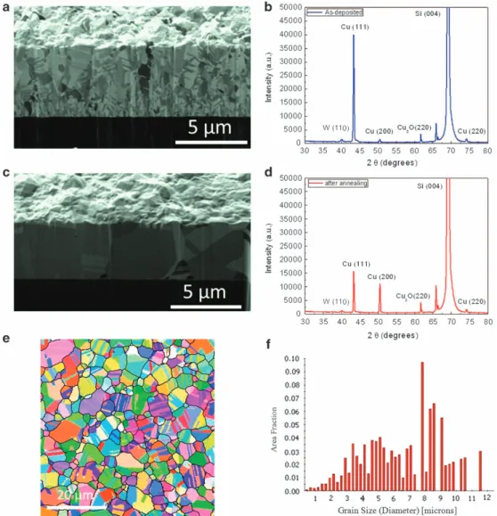
Figure 9 Normal grain growth in Cufilms without o1114-oriented nt-Cu. (a) Cross-sectional focused ion beam (FIB) image for the as-fabricated Cu film at 200 mA cm− 2. (b) The corresponding X-ray diffraction spectrum for the Cufilm in a. (c) Cross-sectional FIB image for the Cu film after annealing at 450 °C for 30 min and (d) the corresponding X-ray diffraction spectrum for the Cufilm in c. (e) Plan-view of the inverse pole figure map from electron backscattered diffraction for the Cu grains annealed at 450 °C for 30 min. (f) Grain size distribution for the grains in e. The average grain size is only 6.6μm, which is approximately the thickness of the Cufilm.
study. Figure 8e and Supplementary Figure S4 showo1004 grains grown to 170 and 207μm, respectively, after annealing at 400 °C for 20 min.
To determine whether theo1114-oriented nanotwins are essential in achieving the extremely anisotropic growth ofo1004 crystals, we prepared randomly oriented nanotwins; however, no extremely abnormal grain growth was observed. Figure 9a presents a FIB cross-sectional view of the randomly oriented nanotwins in Cu, and Figure 9b presents the corresponding X-ray diffraction spectrum, where the {111}, {200} and {220} reflections of Cu are observed. After annealing at 450 °C for 30 min, normal grain growth occurred. Figures 9c and d present the FIB cross-sectional image and the corresponding X-ray diffraction spectrum, respectively. In addition, an inverse pole figure map of the top view of the grains obtained from EBSD in Figure 9e reveals no extremely anisotropic grains. Figure 9f presents a histogram of the grain size distribution that reveals that the average grain size is 6.6μm.
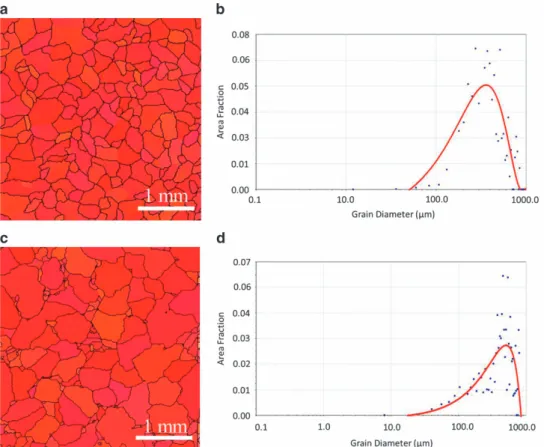
Statistical analysis on the grain size distribution was performed for theo1004 Cu grains transformed from o1114 oriented nt-Cu on Si substrates. Figure 10a presents the plan-view of the inverse pole figure map from EBSD for the o1004 Cu grains after the annealing at 400 °C for 1 h. The average misorientation angle was 3.0° for the grains in Figure 10a, as illustrated in Supplementary Figure S5a. There were 738 grains analyzed for this condition. Figure 10b illustrates the fitting of grain size distribution for the crystals annealed at 400 °C for 1 h, which reveals a normal grain size distribution and not a bimodal distribution. Figure 10c presents the plan-view of the inverse pole
figure map from EBSD for the o1004 Cu crystals annealed at 450 °C for 1 h. The average misorientation angle was 2.8° for the grains in Figure 10c, as illustrated in Supplementary Figure S5b. We analyzed 743 Cu grains in this condition. The fitting of the grain size distribution for the crystals annealed at 450 °C for 1 h is shown in Figure 10d. Theo1004 Cu grains in this condition also exhibit a normal grain size distribution.
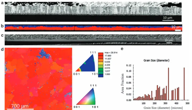
In contrast, in Supplementary Figures S3a and b, we present two connecting images of the cross-section of a sample annealed at 450 °C for 15 min, where the entire sample has been completely transformed into o1004-oriented grains. In Figure 5d, a plan-view of the top surface is shown with respect to the inverse polefigure map. The color of all of the grains is nearly identical, which indicates that all of the grains areo1004 oriented and that the grain size distribution of the o1004-oriented grains is very narrow. The average misorientation angle was 4.7° for the grains in Figure 5d, as illustrated in Supplementary Figure S5c. The average grain size is ~ 283μm, and the largest grain was ~ 470μm, as revealed by the histogram of the grain size provided in Figure 5e. The microstructure of a sample before annealing is presented in Figure 1 and Supplementary Figure S1a, where the average grain size is only ~ 2.4μm.
We define the necessary and sufficient conditions to obtain extremely anisotropic crystal growth below. The first condition is a high density ofo1114-oriented nanotins, which provide the stored energy to serve as the driving force in the growth of the anisotropic and untwinned {100} single crystals. Randomly oriented nanotwins will not do serve as this driving force. The second condition is the
Figure 10 Statistical analysis on grain size distribution for theo1004 Cu grains transformed from o1114-oriented nt-Cu on Si substrates. (a) Plan-view of the inverse polefigure map from electron backscattered diffraction (EBSD) for the o1004 Cu grains after annealing at 400 °C for 1 h. There were 738 grains analyzed in this condition. (b) Fitting of grain size distribution for the crystals annealed at 400 °C for 1 h. (c) Plan-view of the inverse polefigure map from EBSD for theo1004 Cu crystals annealed at 450 °C for 1 h. We analyzed 743 Cu grains in this condition. (d) Fitting of grain size distribution for the crystals annealed at 450 °C for 1 h. Theo1004 Cu grains in both conditions exhibit a mono-sized distribution.
presence of a seeding layer with a low density ofo1004-oriented seeds. When we prepared a seeding layer with a very high density of oriented seeds, we obtained a very high intensity of o1114-oriented nt-Cu; however, upon annealing, we could hardly detect the growth of o1004 grains because there were no o1004-oriented seeds. The third condition is that the substrate should have a large difference in thermal expansion coefficient from that of the metal film, such that a biaxial strain in the in-plane directions of thefilm occurs under high-temperature annealing.
It is well known that abnormal grain growth in Cu has been explained by strain relaxation. Strain will clearly have a role in this study of extremely abnormal grain growth. In addition to the biaxial thermal strain mentioned above, it has been reported that in pulse-electroplating nt-Cu, in situ strain measurement using the bending beam method reveals that the nt-Cufilm is under in-plane biaxial tensile strain.23We
will not attempt to explain the mechanism of abnormal grain growth here because what we have is the microstructural evolution of an elastically anisotropic inclusion (a two-dimensional grain) within an elastically anisotropic matrix (the oriented nt-Cu).
In summary, we report an extremely abnormal grain growth of o1004-oriented single crystals of Cu in a matrix of o1114-oriented and nt-Cu columnar grains; the lateral growth is approxi-mately two orders of magnitude faster than the vertical growth. We have applied this anisotropic growth to produce an array of numerous o1004-oriented single crystals of Cu microbumps with sizes from 100 to 25μm on Si wafer surfaces.
CONFLICT OF INTEREST
The authors declare no conflict of interest.
ACKNOWLEDGEMENTS
Financial support from the Ministry of Science and Technology, Taiwan under the contracts 99–2221-E-009-040-MY3 and 100-2628-E-006-024-MY3 is acknowledged. We would also like to thank the Center for Micro/Nano Science and Technology at National Cheng Kung University for assistance with the analytical equipment.
1 Humphreys, F. J. & Hatherly, M. Recrystallization and Related Annealing Phenomena (Elsevier: Oxford, UK, 2004).
2 Flack, R. D. Fundamentals of Jet Propulsion with Applications Ch. 8 (Cambridge Univ. Press: New York, NY, USA, 2005).
3 Burke, J. E. & Turnbull, D. Recrystallization and grain growth. Prog. Metal Phys. 3, 220–292 (1952).
4 Hillert, M. On the theory of normal and abnormal grain growth. Acta Metall. 13, 227–238 (1956).
5 Thompson, C. V. Grain growth in thinfilms. Ann. Rev. Mater. Sci. 20, 245–268 (1990). 6 Thompson, C. V. Grain growth and evolution of other cellular structures. Solid state
physics. Adv. Res. Appl. 55, 269–314 (2001).
7 Holm, E. A. & Foiles, S. M. How grain growth stops: a mechanism for grain-growth stagnation in pure materias. Science 328, 1138–1141 (2010).
8 Rupert, T. J., Gianola, D. S., Gan, Y. & Hemker, K. J. Experimental observations of stress-driven grain boundary migration. Science 326, 1686–1690 (2009). 9 Schmidt, S., Nielsen, S. F., Gundlach, C., Margulies, L., Huang, X. & Jensen, D. J.
Watching the growth of bulk grains during recrystallization of deformed metas. Science 305, 229–232 (2004).
10 Offerman, S. E., van Dijk, N. H., Sietsma, J., Grigull, S., Lauridsen, E. M., Margulies, L., Poulsen, H. F., Rekveldt, M. Th & van der Zwaag, S. Grain nucleation and growth during phase transformations. Science 298, 1003–1005 (2002).
11 Gusak, A. M. & Tu, K. N. Theory of normal grain growth in normalized size space. Acta Mater. 51, 3895–3904 (2003).
12 Gangulee, A. & D'Heurle, F. M. Anomalous large grains in alloyed aluminumfilms I. Secondary grain growth in aluminum-copper films. Thin Solid Films 12, 399–402 (1972).
13 Gangulee, A. & D'Heurle, F. M. Anomalous large grains in alloyed aluminumfilms II. Electromigration and diffusion infilms with very big grains. Thin Solid Films 16, 227–236 (1973).
14 Greiser, J., Muller, D., Mullner, P., Thompson, C. V. & Arzt, E. Growth of giant grains in silver thinfilms. Scripta Mater. 41, 709–714 (1999).
15 Greiser, J., Mullner, P. & Arzt, E. Abnormal growth of giant grains in silver thinfilms. Acta Mater. 49, 1041–1050 (2001).
16 Koike, J., Wada, M., Sanada, M. & Maruyama, K. Effects of crystallographic texture on stress-migration resistance in copper thin films. Appl. Phys. Lett. 81, 1017–1019 (2002).
17 Nucci, J. A., Keller, R. R., Field, D. P. & Shacham-Diamand, Y. Grain boundary misorientation angles and stress-induced voiding in oxide passivated copper inter-connects. Appl. Phys. Lett. 70, 1242–1244 (1997).
18 Hsiao, H. Y., Liu, C. M., Lin, H. W., Liu, T. C., Lu, C. L., Huang, Y. S., Chen, C. & Tu, K. N. Unidirectional growth of microbumps on (111)-oriented and nanotwinned copper. Science 336, 1007–1010 (2012).
19 Lui, G. T., Chen, D. & Kuo, J. C. EBSD characterization of twinned copper using pulsed electrodeposition. J. Phys. D. Appl. Phys. 42, 215410 (2009).
20 Suh, J. O., Tu, K. N. & Tamura, N. Dramatic morphological change of scallop-type Cu6Sn5 formed on (001) single crystal copper in reaction between molten SnPb solder and Cu. Appl. Phys. Lett. 91, 051907 (2007).
21 Mo, L. P., Wu, F. S., Liu, C. Q. & Xia, W. S. in IEEE Elec. Comp. Tech Conf. 839–843 (IEEE: San Diego, CA, USA, 2012).
22 Li, Q. Q. & Chan, Y. C. Growth kinetics of the Cu3Sn phase and void formation of sub-micrometre solder layers in Sn–Cu binary and Cu–Sn–Cu sandwich structures. J. Alloy. Compd. 567, 47–53 (2013).
23 Xu, D., Sriram, V., Ozolins, V., Yang, J. M., Tu, K. N., Stafford, G. R. & Beauchamp, C. In situ measurements of stress evolution for nanotwin formation during pulse electro-deposition of copper. J. Appl. Phys. 105, 023521 (2009).
This work is licensed under a Creative Commons Attribution-NonCommercial-NoDerivs 3.0 Unported License. The images or other third party material in this article are included in the article’s Creative Commons license, unless indicated otherwise in the credit line; if the material is not included under the Creative Commons license, users will need to obtain permission from the license holder to reproduce the material. To view a copy of this license, visit http://creativecommons.org/licenses/by-nc-nd/3.0/