Fabrication and Characteristics of RF Magnetron Sputtered ITO Thin Films
Wen-Fa Wu and Bi-Shiou ChiouDepartment ofElectronics Engineering and Institute of Electronics, National Chiao Twig University, Hsinchu, Taiwan
ABSTRACT
Indium tin oxide (ITO) films have been deposited onto glass substrates by ifmagnetronsputtering without
in-situ substrate heating. The as-deposited films have an electrical resistivity of 5x
1O
a-cm, visible transmittance of about 85%, and infrared (IR) reflectance of above 80% at 5 jim. The effect of sputtering parameters on the deposition rate and the electrical and optical properties of ITO films are investigated. Loss of transmittance or blackening for ITO films prepared at high spuuering power are observed and explored.1. INTRODUCTION
In recent years, transparent conductive indium tin oxide (ITO) films have been extensively used in a variety of electronic and optoelectronic industries due to their high transmission in visible range, high infrared reflection, and low electrical resistivity [1-5]. The need for ITO films that have both low electrical resistivity and high transparency tn the visible part ofthe solar spectrum has led to the development ofvarious deposition techniques. Both vacuum technques, e.g., sputtering [1-3,6-18] and evaporation [19,201, and non-vacuum techniques, e.g., spray pyrolysis [4,5J and s;reen-printing [2 1J, have been used. Magnetron spuuering can deposit films over large areas at rates comparable to electron-beam evaporation without the degree of radiation heating typical of thermal sources. The deposition rates of magnetron spuftering are higher than those for conventional radio frequency sputtering and a wide range of materials can be deposited [221. Magnetron sputtering is considered to be one of the best methods for preparing ITO films. High quality ITO films prepared by magnetron sputtering have been reported [1,6-16J.
The properties of ifsputtered ITO films are quite sensitive to sputtering parameters, such as substrate temperature [1,3, 14,15], target-to-substrate distance [17], and post-deposition heat treatment [6, 1 1, 141. Although ITO films with both high electrical conductivity and high visible transmittance have been repeatedly obtained. it is
necessary to prepare them at a high temperature (above 350°C) during deposition. Very few authors have discussed high quality ITO films deposited at low substrate temperatures (below 90°C). This paper describes the electric1 and optical properties of ITO films deposited on unheated substrates by an ifmagnetronsputtering apparatus. The eflëct of sputtering parameters on the deposition rate and the optical and electrical properties of ITO films are investigated.
2. EXPERIMENTAL DETAILS
ITO films were prepared by using a commercial ifmagnetronsputtering system (ION TECH, England) Two sorts oftarget were used for the deposition of ITO thin films. One is the self-made target (target A) which was prepared by mixed and pressing reagent-grade In2O3 and SnO2 powders (9Owt% In2O3-lOwt% SnO2) to obtain a sputtering target of 1 inch in diameter and 0. 125 inch in thickness. Another sputtering target (target B) was a 1-in. hot-pressed
oxide ceramics (9Owt% In2O3-lOwt% SnO2) supplied by Superconductive Components, Inc., U.S.A. The subEtrates employed were Corning 02 1 1 or 7059 glass, which were degreased ultrasonically in a diluent detergent solution, rinsed ultrasonically in deionized water, and blown dry in N2 gas before they were introduced into the chamber.
The substrate was fixed above the target with a target-to-substrate distance of 5 cm and a mechanical shutter was attached to the target. High purity Ar (99.999%) was introduced through a mass flow controller after the vacuum chamber was evacuated to about 2x iø6 Torr. The ifpowerwas introduced through an rf power supply (RF Plasma Products, Inc., USA) with an automatic matching network which could be tuned for minimum reflected power. Before
deposition, the target was usually presputtered for 20-30 minutes to remove any contaminants and eliminate any differential sputtering effects. Some specimens were annealing in air at 350 to 550°C for 2 hours alter sputtering.
Film thickness was measured with a stylus profiler. The sheet resistance of the samples was measured with a four point probe and the resistivity of the film was calculated. Carrier concentration and Hall mobility were ob&ained from Hall effect measurement by the Van der Pauw technique. The optical transmittance and reflectance of the films were measured with an ultra violet-visiblenear infrared spectrophotometer (Hitachi U-3410, Japan) and a Fourier transform infrared (FFIR) spectrophotometer.
3. RESULTS AND DISCUSSION
Table I shows the sputtering power dependence of the deposition rate for ITO films prepared at two various sputtering pressures. In ii sputtering, the deposition rate of the films strongly depends on the energy of the sputtered particles arriving at the substrate. The ejected target atoms or molecules undergo collisions with the ambient gas atoms and other sputtered atoms and lose a part of their energy during their transit to the substrate. As the energy of the sputtered atoms or molecules is reduced to the thermal energy ofthe gas kT at a distance h from the targetafter a finite number of collisions, the sputtered atoms or molecules are said to be thermalized [17,231. The distance an atom traveling before being thermalized increases with the increase in the energy of the sputtered atom and with decreising gas pressure. Nyaiesh [24J suggested that a virtual source is expected to form at this distance h. The deposition rate on any surface is lowered as the distance between the virtual source and the surface increases.
For a given argon pressure, the deposition rate increases with increasing ifpower, as shown in Table I.
Similar results were reported in previous works [14,171. The high deposition rate at large sputtering power is aUriuted to the high energy of the sputtered neutrals. The higher sputtering power causes an increase in the density and avrage energy ofthe sputtered neutrals, which would be subjected to a larger number of collisions before they are thermalized. Hence, the position of the Virtual source shifts toward the substrate with increasing sputtering power, the deposition rate is enhanced at high sputtering power, as observed. The deposition rate at an argon pressure of 10 mTorr is smaller than that of 6.5 mTorr as indicated in Table I. At higher argon pressures, there are more collisions between sputtered particles and argon atoms and the energy of the sputtered particles is lowered, resulting in the virtual source moving further away from the substrate. Hence, the deposition rate decreases at higher argon pressures.
Table II exhibits the variation of resistivity, carrier concentration, and Hall mobility with if power for the as deposited ITO films prepared at 6.5-mTorr argon pressure. At an if power of 50-waft, a resistivity of .-5x
l0
-cm is
obtained. Karasawa and Miyata deposited ITO films on unheated substrates by dc reactive sputtering. A resistivity of about 7x10⁴ -cm is reported [18]. Film resistivity decreases as the sputtering power increases. A similar trend have been reported by other researchers [3,171. The decrease in resistivity is due to the combined effect of changes in carrier concentration and Hall mobility. The change in carrier concentration is the dominant factor in this study.The carrier concentration increases and Hall mobility decreases with increasing rf power, as shown in Table II. The increase in sputtering power increases the self-bias at the target, which causes an increase in the density of sputtered neutrals and their average energy. The high energy particles may knock out oxygen atoms, resulting in a reduction in the oxygen content. It is observed that the atomic ratio 0/In of the films is lower than that of the nominal composition and the ratio decreases as the sputtering power increases [9J. The decrease in the oxygen content enhances the presence of oxygen vacancies in the films. The oxygen vacancies act as doubly-ionized donors and contribut two electrons to electrical conduction. Hence, the carrier concentration increases with increasing sputtering power The increase in oxygen vacancies also enhances the scattering ofthe charge carriers and hence the mobility of the cartier is lowered at high sputtering power.
Table III shows the resistivity of as-deposited and annealed ITO films. The as-deposited films were prepared at 25-watt rf power, 20-mTorr argon pressure. Some specimens were annealing in air a 350-550°C for 2 hours after sputtering. The as-deposited film has a resistivity of -3 a-cm as compared to that of '10 )-cm of the 550°C-anrealed specimen. The resistivity of the film decreases as the annealing temperature raises. Similar trend is reported on ITO films annealed in vacuum [16]. The annealing process causes a diffusion of tin atoms from grain boundaries and
interstitial lattice locations to regular 1n203 lattice locations, as tin atom has a higher valency than indium atom does, they behave as donors [1]. In addition, the amorphous structure generally contains levels of localized states lying near the forbidden gap edges in energetic band structure model. These states would act as electron traps. The annealing process causes an increase in the degree of internal order via ciystallization. Consequently, the localized states disappear
and a decrease in resistivity is observed, as shown in Table III.
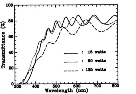
Figure 1 shows the optical transmittance of the as-deposited ITO films prepared at various if power levels. In the visible region of the spectrum, a transmittance ofabout 85% is obtained and the absorption of the films is enhanced as the sputtering power increases. The surface of the film appears grayish at high sputtering power. The oxygen
deficiency in the films is used to explain the loss of transmittance or blackening of ITO films deposited at high sputtering power. It is observed that the oxygen deficiency has contributed to lattice contraction ofthe film and the film becomes more nonstoichiometric at high sputtering power [10].
Figure 2 shows the JR reflectance of the as-deposited ITO films at 5 pin as a function of sputtering power. As shown in Fig. 2, the JR reflectance of the films prepared at a sputtering power of greater than 25 watts increases to more than 80%. The JR reflectance of the ITO films increases at high sputtering power. Frank et a!. [3] showed that the JR reflectance can be expressed by
R=l_4s0C0i
e (1)Ndu
where R is the reflectance, N is the carrier concentration, d is the film thickness, and p is the mobility of th free carriers. According to eq. (1), the IR reflectance increases with the product of carrier concentration N and carrier
mobility p. As discussed previously, films deposited at high sputtering power have lower resistivity and larger value of the product than those deposited at low sputtering power. Hence the IR reflectance ofthe film increases with increasing
sputtering power, as observed.
Figure 3 shows the JR reflectance of ITO films at 5 pm as a function of annealing temperature. The IR
reflectance of the 550°C-annealed film at 5 .tm increases to about 20% higher than that of the as-deposited on .The
infrared reflectance ofthe 550°C-annealed film approaches 60% at 5 pm. The annealed film has smaller resistivity and larger value of the product of carrier concentration N and carrier mobility 4u than the as-deposited film does. Hence, infrared reflectance ofthe annealed film is higher than that ofthe as-deposited film as observed.
4. CONCLUSIONS
Transparent conductive ITO films have been deposited on unheated glass substrates by ifmagnetron sputtering. The deposition rate increases with increasing sputtering power and with decreasing sputtering argon
pressure. This finding is related to the energy of the sputtered particles and the position of the virtual sourcc. The deposition rate on any surface is lowered as the distance between the virtual source and the surface increases. The energy of sputtered particles is high at high sputtering power and low argon pressure. The virtual source thus moves further toward the substrate and hence the deposition rate increases.
The mobility of the carriers decreases and carrier concentration increases with increasing sputtering power. This can be attributed to the decrease in oxygen content of the film as the sputtering power increases. The decrease in
the oxygen content of the films enhances the formation of oxygen vacancies, which contribute two electrons to electrical conduction and enhance the scattering of the charge carriers. Hence, the mobility of the carriers decreascs and carrier concentration increases at high sputtering power. Loss of transmittance and blackening of ITO films prepared at high sputtering power are observed. It is believed that the oxygen deficiency in the film contributes to this effect. The increase of charge carriers causes the IR reflectance to increase as well. High JR reflectance is obtained for films deposited at a sputtering power of higher than 25 watts.
Annealing of ITO-coated substrates at a temperature of 350-550°C for two hours in air causes the tin atoms to be activated and behave as effective donors. The electrical resistivity of ITO film decreases by more than two orders of the magnitude after annealing. The infrared reflectance increases as the annealing temperature is raised.
octz ion 3IdS/ ZZE •LO (9861) 'mfl10UA
'qSiEA
.1 (8L61)ci
'jouqo3j
PS ORAf
8L61'PA
MON 'SSOid OiUJIM31'ssaoj
wjzq u!t/2'U1{
pui
USSOATI
Zt •91I
(c661) S 'jOUM3j•'S
pUOOllUO'1fl3U11
UI
DjijJA4 N'SSS
'uoyq ç jddy'Siq
u
(c661) •LZCIN oz 90Z (6861) ZZ
'SAtj
iddy
:
Siq
f
'uIAwuniqn
y
pirnumuniqnsijj
N•c:i
(66!)
zz
'swi!d PTIOS u!1LL 'ewc!1v\I A Ptfl MSEJ1N.1
.81 •O/21 (6861)9
'Siq
jddyf
'qUiSUE}\J !IiIqy pilE JI?uIRN 1U1SIALAD
•L.1 (8861)8
'U111flOEA'sopiç
pui
Eiqi
66E1 (0661) 8 'VI''1L
1°S"A
1
'E1flUfltBN{
pui
'IWJ A'N°'!11
A 'NSqqSI Sçj
•VN
'ZOUjJtjA.f
jUEIiI
'Z113flflQ lOS13U
'13WJAt 9Z (z661)6O
.t'I
69Z (1661) 6t'ISf 'lOS jddV 'flOUI1IHpui
pjBj
'owS!!S
A E1 (1661)81
mqooipj
•1'SU'j
TH3
.Z1 891 (z661)'uo1o!a
UIiuyq
:1osij,s
'DjOU HPU
O1NS
'I?(O8RjOa 1 .11 j0Uq3Jis
puoorni
01puiwqns
"°"D
pui
flj
O
dA
'M
put?sa
'noiqj
puiuiqnsoi
uujj
PIlOS slulid•6 00S
'-"D
ujy
f
01 pflhiuqns 'TiM put? tpIS}{Is
'11OIID5
89f
i(66i)
6ZZ 'SUijiJ P!1°S UNI 'qoiSjjLS
Pill? '10N3S
dA
M
plJt•S
flØ3
jddy •JJfl5'PS
89(66I)
L61 9 tM! (1861) LL 'Swild P!!S URjj 'UIj1SQ UE I3TWN•[
')JJ
9
czi.. (0861)LZ-U
'S3OIA3Q U011O3j StIt?Jj3I
'qSEuOd •f•SPu
l?ULIt?1ISdd
')IO1ISV S •j7 61L! (cL6!) zzi 'oosuipono
r
'i3uq3t?Id
pu
uj
33f
'13S!OqOHy
'AjSjt?M1q4 tH?3
')Z01JA4StjJ
Sn! !pijo5 'I? (1661) 19fIA! Z 6f1'l (1661)
O
'Scqd jddyf
udf '13131p5 IA! Pill? 'P1P!1A! )1d
1SaDNEIIaU
9
-600I-L1t0-Z8 DSN °N IOEIIUOO)3oi
'UEMU?jjo
Ollll03 30U3105 II?UOnEN31
Aq p3uoddns cjul?d Ul? (910-600 -cl-01Z0-Z8 SDN
!OElluoO)Aojompj
put? 33U3I)5 JO 0111111SU1 Ul?tlS-2UW13 3111q
p3uoddns SI )OM SLjJlNaN9aarIMOMMDV
Table I. Dependence of deposition rate on sputtering power for ITO films prepared at two various sputtering pressures.
Sputtering Power (watts)
Deposition rate (A/mm.)
6.5 mtorr 10 mtorr
15 53.7 23.1
50 271.6 190.7
100 458.3 312
Table II. Electrical properties of the as-deposited ITO films prepared at various sputtering powers. The sputtering source is target B.
Sputtering Power (watts) resistivity ()-cm) mobility (cm2/V-sec) carrier concentration (1/cm3) 15 1.06x10³ 52.04 1.23x10²⁰ 50
4.79x10
36.43 2.07x 10²⁰ 1253.73x10
11.02 3.99x10²⁰Table III. Resistivity of as-deposited and annealed ITO films. The sputtering source is target A.
resistivity
(-cm)
as-deposited film 3.127 350°C-annealed film 5.1 x 10² 550°C-annealed film 9.3 x SPIEVo!. 21501323Fig. 1 Transmittance of the as-deposited ITO films prepared at various sputtering powers.
Fig. 2 JR reflectance of the as-deposited ITO films at 5 m as a function of sputtering power.
I
I
I
80
60
4020
I ...1L
50
100 150Sputtering Power (watts)
' 80
:
20 .a—d.ponited film
0
0
100ilii
200
i .11 I_1 II I 1I
300
400
III
500 600
f I I_
Annealing
Temperature
(°C)
Fig. 3 IRreflectanceat5pinof ITO films as a function of annealing temperature.