C.L. Lai, C.H. Lin, and Chih Chen
Department of Materials Science and Engineering, National Chiao Tung University, Hsin-Chu 300, Taiwan, Republic of China
(Received 7 July 2003; accepted 22 October 2003)
The electromigration behavior of the composite solder composed of eutectic and high-lead SnPb was investigated with 5.7 × 10⁴
A/cm2
current stressing. Voids and hillocks were found only within the eutectic solder, and the high-lead solder remained intact. Electromigration was accelerated dramatically at 150 °C, and Pb became the major migration species of eutectic SnPb for the microstructure change at the anode. The polarity of the opposite current direction was also studied. When electrons drift from the eutectic side to the high-lead side, voids occurred at the eutectic–Cu interface whereas hillocks accumulated at the eutectic–high-lead interface. When the current was reversed, voids occurred at the eutectic–high-lead interface whereas hillocks accumulated at the eutectic–Cu interface. The anchoring effect, which results from the attaching of the lead-rich grains in the eutectic solder to the high-lead solder, was considered to retard the electromigration damage only in this current direction.
I. INTRODUCTION
Electromigration is a crucial concern in the microelec-tronics industry, and since the 1960s it has been found to be the major cause of void formation that can result in the fatal open-circuit-failure.1 Therefore, numerous studies and quantitative modelings on this subject have been carried out.2–4With the miniaturization of integrated cir-cuit design and better performance of chips, higher input/ output density is required for future generations of mi-croelectronic packaging. Among all the packaging tech-nologies, flip-chip technology appears to be one of the most promising solutions for high-density packaging. Currently, solder bumps with about 100m in diameter are stressed by current density of the order 103
A/cm2 . The dimension of the solder joint is expected to approach 50m in the year 2004,5
in which higher current density up to 104 A/cm2 as well as more serious Joule heating would accelerate the electromigration damage. There-fore, electromigration phenomena and failure analysis of various solders and under bump metallurgy (UBM) ma-terials have recently been reported.6–8
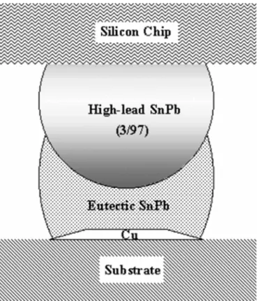
Furthermore, composite bumps of eutectic solders consist of high-lead (Sn–95 wt% Pb) and eutectic SnPb solder bumps on the chip and the substrate side, respec-tively. These bumps are widely used in flip chip attach, direct chip attach, and various ball grid array packaging technologies.9–11 The schematic structure of the bumps is shown in Fig. 1. These composite bumps have their excellent reliability and lower cost due to the organic substrate. Thus, they are used for flip-chip packag-ing in high-performance electronic devices, such as
microprocessors.12 However, as the dimension of the bumps shrinks, electromigration in the composite bumps will become an increasingly important reliability issue. However, no literature on this issue has been found. Con-sequently, this paper examines electromigration behavior in the composite solder joint. Test samples were stressed with different current directions under different tempera-tures to investigate microstructure changes and failure mechanisms. Polarity and temperature effects on the electromigration damage were also inspected.
II. EXPERIMENTAL
To simulate the structure of the composite bumps, a V-shape solder line was used in this study. After a stan-dard cleaning process, a layer of 1200 Å thick oxide film was grown on an n-type four-inch (100) wafer. Then, a silicon nitride film of 1500 Å was deposited on the SiO2 layer by low-pressure chemical vapor deposition to act as a hard mask for subsequent Potassium (KOH) etching. Using lithography and etching, a V-shape groove with 200-m width was obtained. Then, e-beam evaporator was used to deposit UBM on the chip, which consisted of Cr (500 Å), Cu (5000 Å), and Au (500 Å) films.
To prepare the composite joint, the whole wafer was cut into 1 cm × 1 cm square chips with a V-groove in the middle. Afterwards, Cu was electroplated onto the UBM in a CuSO4solution. Then, the chip was polished, and the electroplated copper was left only in the V-groove to serve as a conducting pad and react with SnPb solders. Photolithography was utilized to pattern an open square
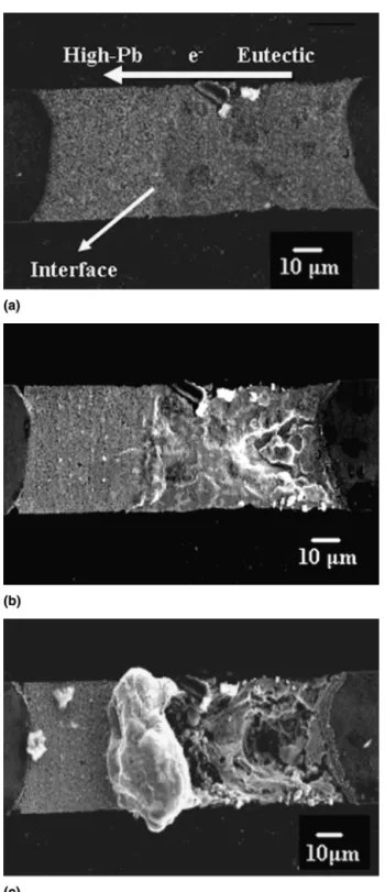
in the middle of the copper line, and then the copper in the square was etched away by FeCl3 solution. Next, high-lead solder paste at the composition of 95 wt% Pb was reflowed into the etched square at 350 °C ± 3 °C on the hot plate for 30 s. Afterwards, photolithography was utilized again to open another square with half the length of the previous high-lead section, and the high-lead por-tion in the square was etched with the etchant (HNO3:CH3COOH:glycerol⳱ 10:10:20). Next, eutectic SnPb solder paste was reflowed into the patterned square at 220 °C ± 3 °C for 30 s. Finally, the sample was polished to a smooth surface. The schematic drawing and scanning electron microscopy (SEM) image of the fab-ricated sample are shown in Figs. 2(a) and 2(b), respec-tively. The whole solder line in the V-groove was con-trolled to be about 150m in length, 50 m in width, and 35m in depth, which is close to the dimension of com-posite solder. In addition, this structure facilitated the observation of the electromigration during stressing.
The V-groove copper line was connected to a power supply on both ends through copper wires. The experi-mental conditions for various samples are shown in Table I. Solder lines that were stressed by 5.7 × 10⁴ A/cm2current density were tested at both room tempera-ture and 150 °C on a hot plate for accelerating tests. In addition, sample 5, which was heated to 150 °C without current stressing, was used to separate the thermal effect and electromigration. To observe the morphology and
composition evolution, the specimens were photographed by either secondary electron (SE) or backscattered elec-tron (BSE) SEM and analyzed by energy dispersive spec-troscopy (EDS) after each appropriate interval of stress-ing time.
III. RESULTS AND DISCUSSION
Electromigration damage was found mainly within the eutectic solder of sample 1, in which the electron flow went from eutectic solder to high-lead solder. The SEM images in Figs. 3(a)–3(e) illustrate the microstructure evolution of the composite solder before and after vari-ous stressing times up to 7 days. Figure 3(a) shows the FIG. 1. Schematic diagram of flip-chip attach joint with the composite
bump.
FIG. 2. (a) Schematic diagram of the V-groove sample prepared on (100) silicon wafer. (b) SE SEM image of the fabricated sample with high-lead solder in the left side and eutectic solder in the right side. In the eutectic solder, the lighter regions represent lead-rich grains and the darker regions represent tin-rich grains.
TABLE I. List of the experimental conditions including the current density, temperature, and current direction.
Testing temperature
Room temperature 150 °C
Current direction Current direction Anode at high-Pb side Anode at eutectic side Anode at high-Pb side Anode at
eutectic side No current Sample 1 Sample 2 Sample 3 Sample 4 Sample 5 All specimens were stressed by 5.7 × 10⁴A/cm2current density. C.L. Lai et al.: Electromigration at the high-Pb–eutectic SnPb solder interface
SEM image of sample 1 before stressing. The arrow in the figure indicates the interface between the high-lead and eutectic solder. After 4-day stressing by 5.7 × 10⁴
A/cm2
at room temperature, the voids initiated near the
eutectic/Cu interface and became progressively larger, as shown in Fig. 3(b). At the same time, hillocks accumu-lated around the eutectic–high-lead interface, as shown in Fig. 3(c). However, no obvious morphological change FIG. 3. SE SEM images showing the microstructure evolution for sample 1: (a) before stressing, (b) high-lead side after 4-day stressing, (c) eutectic side after 4-day stressing, (d) high-lead side after 7-day stressing, and (e) eutectic side after 7-day stressing.
was observed within the high-lead solder and at the in-terface of high-lead solder and the Cu electrode. Because the liquidus temperature of high-lead solder (about 350 °C) is higher than the eutectic temperature of eutectic solder (about 183 °C), the former could be expected to have better electromigration resistance due to smaller diffu-sivities of Sn and Pb at the testing temperature.8
When the stressing time reached 7 days, the sample failed elec-trically. The microstructure after the failure is shown in Figs. 3(d) and 3(e), indicating that the failure was at the eutectic side. From Fig. 3(e), the eutectic solder was al-most fully depleted by electron flow, thus causing the elec-trical open failure. Furthermore, large hillocks were piled up at the interface of high-lead and eutectic solder. Never-theless, the high-lead end remained intact.
To investigate the polarity effect, sample 2 was stressed by a current direction opposite to that in sample 1. In this situation, the electrons drift from high-lead solder to the eutectic solder. After 12 days of current stressing, small hillocks, as shown in Fig. 4(a), began to form at the eutectic–Cu interface. Furthermore, tin-rich grains in the eutectic solder were depleted in the vicinity of the eutectic–high-lead interface, as indicated by the arrow in Fig. 4(b). However, the high-lead end remained unaffected.
To examine the effect of temperature on electromigra-tion, sample 3 was tested at 150 °C with electron flow from the eutectic to the high-lead side. Figures 5(a)–5(c) show the SEM images taken after 0-, 10-, and 24-h cur-rent stressing, respectively. Similar to sample 1, eutectic solder started to deplete at the junction of the eutectic solder and the Cu electrode, as seen in Fig. 5(b). After 24-h stressing, almost all the eutectic solder migrated away from the V-groove, accumulating around the origi-nal eutectic–high-lead interface. In addition, this deple-tion of eutectic solder undoubtedly led to the fatal open failure, and electromigration damage was accelerated dramatically at 150 °C. However, this testing tempera-ture did not influence the high-lead solder and only dam-aged the eutectic side.
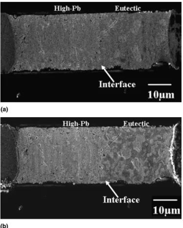
Sample 4 was used to investigate the polarity effect at 150 °C. The SEM images in Fig. 6 show the microstruc-ture evolution at various stages of current stressing. Figure 6(a) represents the microstructure of the sample before stressing, with labels for the high-lead and eutec-tic solders. After electron flow was applied from the high-lead side to the eutectic side for 10 h, the eutectic solder began to be depleted at the interface of high-lead– eutectic solder. In addition, some small hillocks were found at the junction of the eutectic solder and the Cu electrode. After 30-h stressing, the high-lead solder re-mained unchanged under the current stressing, as typical for all of our stressed samples. The depletion at the interface became more serious, and the hillocks and lumps around the anode side grew larger.
The microstructure evolution and phase changes within sample 4 were noteworthy. In Fig. 6(a), the tin-rich regions constituted the matrix phase (continuous phase) in the eutectic SnPb solder after reflow. As the stressing time increased, phase separation continued, and the lead-rich grains in the eutectic solder coarsened. As illustrated from Figs. 6(a) to 6(c), it was significant that the lead-rich phase finally became the matrix, especially within the lump around the eutectic–Cu interface. It was found that there were many lead atoms migrating along the direction of electron flow within the eutectic solder. The tracer diffusion experiment conducted by Gupta et al.13showed that210Pb diffused faster than113Sn in eu-tectic solder due to the change in the microstructure FIG. 4. BSE SEM images showing the microstructure for sample 2 after 12-day stressing. (a) Interface between eutectic solder and Cu of the anode side. (b) Interface between eutectic and high-lead solder. The black particles in the image are the SiC left from polishing.
during annealing at 151 °C. Furthermore, Tu et al.6 con-cluded that lead in eutectic solder is the dominating diffusion species for electromigration at 150 °C. Our experimental results seemed to agree with these studies. At about 150 °C, the lead atoms in eutectic solder play
an important role in the electromigration behavior, in-cluding microstructure changes and atomic redistribu-tion. Besides, the difference of activation energy between Pb and Sn atoms in eutectic solder may also affect the diffusion behavior during electromigration.
FIG. 5. SE SEM images showing the microstructure evolution for sample 3: (a) before stressing, (b) stressed after 10 h, and (c) stressed after 24 h to failure. Analysis by EDS indicated that the particles on the high-lead solder were analyzed to be the dust instead of hillocks.
FIG. 6. SEM images of sample 4: (a) before stressing, SE image; (b) after 10-h stressing, SE image; (c) BSE image photographed after 30-h stressing to show the dramatic evolution of the phase distribution; and (d) the averaging Pb concentration profile measured from the EDS line scanning.
However, sample 4 was found to have better electro-migration resistance than sample 3. This polarity effect can be attributed to the electromigration behavior around the high-lead–eutectic interface. The enlarged image at the interface is shown in Fig. 7. It was noteworthy that the solder left in the interface was the lead-rich phase. As seen in Figs. 6(b) and 6(c), with more current stressing, there was more depletion of trich phase near the in-terface. This also can be verified from the average con-centration profile shown in Fig. 6(d). Average concen-tration of Pb atoms at a specific position was obtained by EDS line scan along the width direction of the sample. Starting from the interface of Cu electrode and eutectic SnPb solder, line scans were performed approximately every 7m along the length direction of the sample to obtain the concentration profile of Pb. Around the inter-face, Pb concentration clearly increased after 30-h stress-ing. However, most of the lead-rich grains stayed at the interface. This depletion behavior seemed to contradict the above discussion, as Pb atoms are the dominating diffusion species at 150 °C. It was speculated that this interfacial electromigration behavior may result from the following mechanism below. The lead-rich grains within the eutectic solder can be regarded as small pieces of high-lead solders dispersed in the eutectic solder. When the eutectic solder was reflowed into the V-groove, these small high-lead solders near the interface tended to attach to the high-lead solder side. Therefore, the lead-rich grains near the interface became a part of the high-lead solder. Because high-lead SnPb can resist electromigra-tion very well under these testing condielectromigra-tions, these high-lead grains almost did not migrate during current stress-ing. It was believed that this “anchoring effect” strength-ened the interface, and thus provided more resistance to electromigration when electrons drift from high-lead to eutectic solders.
To clarify the change caused by electromigration only, sample 5 was annealed at 150 °C for 24 h. Figures 8(a) and 8(b) show the SEM images of this sample before and after the heat treatment, respectively. High-lead grains apparently ripened in the eutectic solder. In addition, the tin-rich and lead-rich phases had almost reached equilib-rium thermodynamically when solidified. Therefore, there was no significant Pb diffusion from high-lead to eutectic solder due to concentration gradient in the eu-tectic alloy system, as observed in this annealed sample. Furthermore, these phenomena occurred only in the 150 °C cases, not in the room temperature cases. Hence, one can conclude that grain ripening at higher temperatures can mainly be attributed to the thermal effect rather than electromigration. Furthermore, Fig. 8(b) shows that the lead-rich regions near the eutectic–high-lead interface tended to attach to the high-lead solder whereas the tin-rich phase remained the matrix phase. This was substan-tial evidence of the “anchoring effect.”
Based on the above results, it is concluded that high-lead solder has better electromigration resistance than eutectic solder, which can be attributed to its higher liq-uidus temperature that results in lower diffusivities of Sn and Pb atoms. For composite solder lines, the electrical open occurred due to failure caused by severe void for-mation within the eutectic solder. In addition, eutectic
FIG. 7. Enlarged BSE SEM image of sample 4 at the eutectic and high-lead interface.
FIG. 8. SE SEM images of sample 5: (a) before annealing, and (b) after 24-h annealing.
solder depletion was prone to occur around the interface, either the eutectic–high-lead or the eutectic–Cu interface, and extending gradually into the whole eutectic solder.
It is discovered that the anchoring effect would alle-viate the void formation around the eutectic–high-lead interface to some extent when electrons drift from eutec-tic solder to high-lead solder. However, if the electron flow is reversed, the copper, which corresponds to UBM in the flip chip, does not contribute toward this effect. The eutectic solder adheres to the copper only by the formation of intermetallic compounds, so that the voids might form more easily. By comparing the cases with different current directions at the same temperature (room temperature or 150 °C), it is shown that anchoring effect could retard the electromigration damage. In con-clusion, the composite solder with electron flow from the high-lead side to the eutectic side is expected to resist electromigration failure better.
IV. SUMMARY
Electromigration in high-lead–eutectic composite sol-der lines has been studied unsol-der the current density of 5.7 × 10⁴A/cm2. When electrons drifted from the high-lead side to the eutectic side, voids occurred at the eu-tectic–high-lead interface, whereas hillocks accumulated at the eutectic–Cu interface. The “anchoring effect” would retard electromigration damage. When electrons drifted from eutectic side to high-lead side, voids oc-curred at the eutectic–Cu interface, whereas hillocks ac-cumulated at the eutectic–high-lead interface. Electromi-gration can more easily ruin the composite solder under this current direction. Open failure was found within the eutectic solder for samples 1 and 3, and this failure was mainly due to electromigration. The high-lead solder ex-hibited better electromigration resistance than the eutec-tic solder.
The important thermal and polarity effects were also
examined. Higher temperatures would enhance the rate of electromigration and the grain coarsening. It also dra-matically shortened the lifetime of solder intercon-nections. In addition, lead became a noticeable diffu-sion species in eutectic SnPb alloy during electromigra-tion at 150 °C.
ACKNOWLEDGMENTS
The authors would like to thank professor K.N. Tu for helpful and insightful comments as well as the National Science Council, Taiwan, Republic of China, for finan-cial support under Grant No. NSC 89-2218-E-009-109.
REFERENCES
1. H.B. Huntington and A.R. Grone, J. Phys. Chem. Solids 20, 76 (1961).
2. I.A. Blech, J. Appl. Phys. 47, 1203 (1976).
3. R. Landauer and James W.F. Woo, Phys. Rev. B10, 4, 1266 (1974).
4. K.N. Tu, Phys. Rev. B 45, 1409 (1992).
5. International Technology Roadmap for Semiconductors (Semi-conductor Industry Association, San Jose, CA, 1999).
6. Q.T. Huynh, C.Y. Liu, Chih Chen, and K.N. Tu, J. Appl. Phys. 89, 4332 (2001).
7. T.Y. Lee, K.N. Tu, S.M. Kuo, and D.R. Frear, J. Appl. Phys. 90, 4502 (2001).
8. C.Y. Liu, Chih Chen, and K.N. Tu, J. Appl. Phys. 88, 5703 (2000).
9. D.O. Powell, and A.K. Trivedi, in Proc. 43rd Electronic Compo-nents and Technology Conference, IEEE CompoCompo-nents, Packaging and Manufacturing Technology Society, Orlando, FL, 1993, pp. 182–186.
10. R.K. Doot, in Proc. 46th Electronic Components and Technology Conference, IEEE Components, Packaging, and Manufacturing Technology Society, Orlando, FL, 1996, pp. 535–539.
11. J.H. Lau, Ball Grid Array Technology (McGraw-Hill, New York, 1995).
12. R. Shukla, V. Murali, and A. Bhansali, in Proc. 49th Electronic Components and Technology Conference, IEEE Components, Packaging, and Manufacturing Technology Society, Orlando, FL, 1999, pp. 945–949.