IEEE ELECTRON DEVICE LETTERS, VOL. 24, NO. 7, JULY 2003 457
Investigation of Grain Boundary Control in the Drain
Junction on Laser-Crystalized Poly-Si Thin
Film Transistors
Tien-Fu Chen, Ching-Fa Yeh, and Jen-Chung Lou
Abstract—This letter investigates the influences of grain bound-aries in the drain junction on the performance and reliability of laser-crystalized poly-Si thin film transistors (TFTs). A unique test structure where the channel region includes 150-nm-thick laser-crystalized poly-Si with small grain sizes and a 100-nm-thick one with large grain sizes is fabricated. Different behaviors in the elec-trical characteristics and reliability of a single TFT are observed, first under measurements of the forward mode and then under measurements of the reverse mode. This is due to the different number of grain boundaries in the drain junction. Grain bound-aries in the drain junction were found to cause reduced ON/OFF current ratio, variations in threshold voltage with drain bias, sig-nificantly increased kink effect in the output characteristics, and poor hot-carrier stress endurance.
Index Terms—Drain junction, electrical characteristics, grain boundaries, kink effect, laser-crystalized poly-Si, reliability.
I. INTRODUCTION
L
ASER-ANNEALED polycrystalline silicon thin film tran-sistors (poly-Si TFTs) have widely been explored owing to their possibilities for integrating peripheral driver circuits with active matrix liquid crystal displays (AMLCDs) on large area glass substrates [1]. To achieve system on glass (SOG), poly-Si TFTs with high carrier mobility and good reliability are required [2]. Several techniques have been proposed for enhancing car-rier mobility, such as enlarging the grains in the channel, and improving their reliability by reducing the electric field near the drain [3], [4].However, the random distribution of the grain boundaries (GBs) in the channel impairs device performance uniformity. The influence of the grain-boundary location on the poly-Si TFTs was first considered from the data obtained in two-di-mensional (2-D) device simulations [5]. To further control the performance of laser-crystalized poly-Si TFTs, the number of GBs in the drain junction have to be considered. In this letter, a TFT is fabricated that includes two different grain sizes of the laser-crystalized polysilicon in the channel. To avoid de-vice-to-device variations, such as the difference in the number of GBs in the channel, and the channel shortening effect due to the diffusion of dopants from source and drain, this study adopted the measurements from both the forward and reverse Manuscript received March 3, 2003; revised April 7, 2003. This work was supported by the National Science Council of Taiwan, R.O.C. under Contract NSC91-2215-E-009-050. The review of this letter was arranged by Editor J. Sin. The authors are with the Institute of Electronics, National Chiao-Tung Uni-versity, Hsinchu 300, Taiwan, R.O.C. (e-mail: [email protected]).
Digital Object Identifier 10.1109/LED.2003.814007
Fig. 1. (a) Key processes for fabricating this test structure showing source and drain region in relation to the channel thickness under measurements of forward mode. (b) SEM photograph of laser-crystalized poly-Si after Secco etching.
modes in a single TFT [6]. The purpose in taking this approach was to study the influences of the GBs in the drain junction on the performance and reliability of laser-annealed poly-Si TFTs. Behaviors differed between the forward and reverse modes because of the different number of GBs in the drain junction.
II. EXPERIMENT
The key processes to fabricate this test structure are displayed in Fig. 1(a). First, a 50-nm-thick amorphous silicon layer was deposited on thermally oxided (2- m thick) Si wafers by de-composing SiH in LPCVD system at 550 C. Next, a 150-nm-thick silicon nitride layer was deposited and then patterned. The exposed silicon film was fully oxidized at 925 C using silicon nitride patterns as a hard mask. Meanwhile, the silicon nitride patterns were selectively etched in a hot phosphoric acid bath 0741-3106/03$17.00 © 2003 IEEE
458 IEEE ELECTRON DEVICE LETTERS, VOL. 24, NO. 7, JULY 2003
at 165 C. After removing the native oxide on silicon film re-gion, a 100-nm amorphous silicon layer was deposited by the decomposition of SiH in LPCVD system at 550 C. The wafer was then placed on a 400 C stage in a vacuum chamber under pressure of Torr. The crystallization of amorphous silicon layer was carried out by irradiation using the KrF excimer laser. After defining the active channel region, a 135-nm-thick TEOS gate oxide was deposited by PECVD at 350 C. Subsequently, a 250-nm amorphous silicon layer was deposited and then pat-terned as the gate electrode. The source and drain regions were formed by self-aligned ion implantation of phosphorous with a dosage of cm at 50 KeV. A 300-nm TEOS passiva-tion oxide was deposited, and then the dopants were activated at 600 C for 12 h. Finally, contact opening and metallization were performed. No further hydrogenation procedures were im-plemented after sintering at 400 C for 30 min.
As shown in Fig. 1(a), the heavily doped region near the 100-nm-thick channel side is defined as drain when a TFT is measured in the forward mode. The other is defined as drain under measurements of the reverse mode. The channel length comprises 150-nm thick channel length and 100-nm-thick channel length . A margin of 0.5 m is assigned for the proposed TFTs, as presented in Fig. 1(a). The laser energy densities between completely melting 100-nm-thick silicon film and partially melting a 150-nm one were employed to form two different grain sizes of laser-crystalized polysilicon [3]. Meanwhile, Fig. 1(b) displays the SEM photograph of laser-crystalized poly-Si. Large and small grains are formed in the channel simultaneously. The different number of GBs in the drain junction are exhibited under measurements of the forward and reverse modes.
III. RESULTS ANDDISCUSSION
Fig. 2 illustrates the transfer characteristics of the laser-crys-talized poly-Si TFT under first forward and second reverse mode. Notably, the leakage current in the reverse mode is sig-nificantly higher than that in the forward mode. This increase in the leakage current results from the marked increase of the GBs in the drain junction [7]. Many carriers generated from the GBs via thermionic-field emission result in higher leakage current in the reverse mode than the forward mode. The on-currents are almost identical for both mode measurements because of the TFT operated in linear region. Therefore, the order of magnitude in the on/off current ratio is reduced at high drain bias in the reverse mode compared to the forward mode. Fig. 2 also indicates that the threshold voltage which is defined as the gate bias for a drain current of nA, is 5.78
and 5.20 V in the reverse mode at and V,
respectively. However, the is maintained at 5.90 V for
both V and V in the forward mode. The
reduction in in the reverse mode results from the avalanche induced short channel effect [8]. This effect is not observed in the forward mode, because the drain junction contains large grains and fewer GBs.
As shown in Fig. 3, the kink effect which causes a rapid in-crease in drain current appears more prominently in the reverse mode than in the forward mode [9]. This phenomenon can be
Fig. 2. Transfer characteristics of the laser-crystalized poly-Si TFT under forward and reverse mode measurements in one TFT.
Fig. 3. Output characteristics of the laser-crystalized poly-Si TFT under forward and reverse mode measurements in one TFT.
attributed to the drain induced grain-boundary barrier lowering effect and the grain-boundary traps induced avalanche genera-tion effect [10], [11]. The former effect is caused by the drain bias modulating the barrier height of the GBs in the drain junction to form an asymmetric barrier. Extra carriers which are injected from the lowered barrier side into the drain side cause the drain current to increase with the drain voltage [12]. The latter effect results from the higher electric field created by grain-boundary traps in the drain junction. Electron-hole pairs are generated by the impact ionization process, resulting in a lack of saturation in the output characteristics [13].
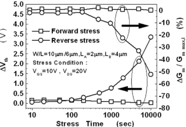
Fig. 4 shows the threshold voltage variations and the degradation of the maximum transconductance in a single TFT under static hot-carrier stress which is defined as the TFT being kept at a high electric field in the drain junction. The TFT is first stressed in the forward mode and then in the reverse mode. Notably, the dc stress conditions
are V and V for 10 000 s. The is
defined as - where denotes the initial and
represents the for etch stress time. Moreover, the
degradation of the is defined as ,
where denotes the
initial and represents the for each
stress time. The and are measured at
V for etch stress time. One can see that the and the are virtually unchanged in the forward stress but are strongly degraded in the reverse stress. This effect occurs due to the higher electric field at the drain junction in the reverse exceeding that in the forward mode. Notably, the high
CHEN et al.: INVESTIGATION OF GRAIN BOUNDARY CONTROL 459
Fig. 4. Threshold voltage variation and degradation of maximum transconductance under static hot-carrier stress in a single TFT. The TFT is first stressed in the forward mode, and then second stressed in the reverse mode. Meanwhile, the threshold voltage V is defined as a drain current of(W=L) 2 10 A atV = 0:1 V.
electric field promotes impact ionization, resulting in numerous grain-boundary traps being created in the drain junction.
IV. CONCLUSION
This investigation has demonstrated that GBs in the drain junction seriously impedes the performance and reliability of the laser-crystalized poly-Si TFTs. Grain-boundary traps in the drain junction boosted the leakage current, caused threshold voltage to vary with drain bias, enhanced the kink effect in the output characteristics, and degraded device performance under static hot-carrier stress. These effects are attributed to the high local electric field in the drain junction.
ACKNOWLEDGMENT
The authors would like to thank the Nano Facility Center (NFC) of National Chiao-Tung University, and the National
Nano Device Laboratory (NDL) for providing process equip-ment.
REFERENCES
[1] N. Sasaki, A. Hara, F. Takeuchi, Y. Mishima, T. Kakehi, K. Yoshino, and M. Takei, “High throughput CW-laser lateral crystallization for low-temperature poly-Si TFT’s and fabrication of 16 bit SRAM’s and 270 MHz shift registers,” in SID Tech. Dig., 2002, pp. 154–157.
[2] Y. Matsueda, S. Inoue, and T. Shimoda, “Concept of system on panel,” in AMLCD Tech. Dig., 2001, pp. 77–80.
[3] C.-W. Lin, L.-J. Cheng, Y.-L. Lu, Y.-S. Lee, and H.-C. Cheng, “High-performance low-temperature poly-Si TFT’s crystallized by eximer laser irradiation with recessed-channel structure,” IEEE Elec-tron Device Lett., vol. 22, pp. 269–271, June 2001.
[4] C.-W. Lin, C.-H. Tseng, T.-K. Chang, C.-W. Lin, W.-T. Wang, and H.-C. Cheng, “A novel laser-processed self-aligned gate-overlapped LDD poly-Si TFT,” IEEE Electron Device Lett., vol. 23, pp. 133–135, Mar. 2002.
[5] M. Kimura, S. Inoue, and T. Shimoda, “Dependence of polycrystalline silicon thin-film transistor characteristics on the grain-boundary loca-tion,” J. Appl. Phys., vol. 89, pp. 596–600, 2001.
[6] C. A. Dimitriadis, P. A. Coxon, and N. A. Economou, “Influence of de-position pressure on the output characteristics of low pressure chem-ical vapor deposited polycrystalline silicon thin-film transistors,” Appl. Phys. Lett., vol. 63, pp. 943–945, 1993.
[7] I.-W. Wu, A. G. Lewis, T.-Y. Huang, W. B. Jackson, and A. Chiang, “Mechanism and device-to-device variation of leakage current in polysilicon thin film transistors,” in IEDM Tech. Dig., 1990, pp. 867–870.
[8] S. Yamada, S. Yokoyama, and M. Koyanagi, “Two-dimensional device simulation for avalanche induced short channel effect in poly-Si TFT,” in IEDM Tech. Dig., 1990, pp. 859–862.
[9] K. P. A. Kumar, K. O. S. Johnny, T. N. Cuong, and K. K. Ping, “Kink-free polycrystalline silicon double-gate elevated-channel thin-film transis-tors,” IEEE Trans. Electron Devices, vol. 45, pp. 2514–2520, Dec. 1998. [10] H.-L. Chen and C.-Y. Wu, “A newI-V model considering the im-pact-ionization effect initiated by the DIGBL current for the intrinsic
n-channel poly-Si TFT’s,” IEEE Trans. Electron Devices, vol. 46, pp.
722–728, Apr. 1999.
[11] M. Hack and A. G. Lewis, “Avalanche-induced effects in polysilicon thin-film transistors,” IEEE Electron Device Lett., vol. 12, pp. 203–205, May 1991.
[12] C. A. Dimitriadis and D. H. Tassis, “Output characteristics of short-channel polycrystalline silicon thin-film transistors,” J. Appl. Phys., vol. 77, pp. 2177–2183, Mar. 1995.
[13] G. A. Armstrong, S. Uppal, S. D. Brotherton, and J. R. Ayres, “Mod-eling of laser-annealed polysilicon TFT characteristics,” IEEE Electron Device Lett., vol. 18, pp. 315–318, 1997.