This content has been downloaded from IOPscience. Please scroll down to see the full text.
Download details:
IP Address: 140.113.38.11
This content was downloaded on 25/04/2014 at 16:59
Please note that terms and conditions apply.
Small GaN-based light-emitting diodes with a single electrode pad fabricated on a sapphire
substrate
View the table of contents for this issue, or go to the journal homepage for more 2008 Semicond. Sci. Technol. 23 045013
(http://iopscience.iop.org/0268-1242/23/4/045013)
Semicond. Sci. Technol. 23 (2008) 045013 (5pp) doi:10.1088/0268-1242/23/4/045013
Small GaN-based light-emitting diodes
with a single electrode pad fabricated on a
sapphire substrate
Y C Lee, C E Lee, T C Lu, H C Kuo and S C Wang
Department of Photonics and Institute of Electro-Optical Engineering, National Chiao Tung University, Hsinchu, 300, Taiwan, Republic of China
E-mail:[email protected]
Received 24 May 2007, in final form 12 February 2008 Published 20 March 2008
Online atstacks.iop.org/SST/23/045013 Abstract
Small-scale GaN-based LEDs with a single electrode pad enjoying such properties as low cost, low series resistance, high efficiency and high yield were fabricated on a sapphire substrate by a novel and simple method. The devices present not only lower series resistance but higher light output power due to a specific n-contact design and better current spreading properties. Furthermore, higher ESD resistance (>−800 V at machine-mode operation) was
demonstrated. The single-pad electrode of small-scale GaN-based LEDs has a chip size of 180× 180 µm2, and showed a lower forward voltage of 3.15 V and 53.4% output power enhancement at 20 mA.
(Some figures in this article are in colour only in the electronic version)
1. Introduction
Recently, wide-bandgap GaN-based light-emitting diodes (LEDs) have attracted significant attention in many different applications [1]. These wide-bandgap GaN-based materials have been used to develop high-performance optical devices [2, 3]. The available substrate options for growing these wide-bandgap materials are GaN, SiC, ZnO and sapphire substrates. Among them, sapphire substrates have advantages such as low-cost and mature epitaxy technology properties. However, an epi-layer grown on a sapphire substrate will limit the flexibility of device processes and end up with a lateral conductive structure design due to the non-conductive sapphire substrate. The lateral structure will further limit device performances such as lower efficiency because most of the light emitting areas are covered by electrode pads which baffle the light output, especially in small chip size. In addition, the small chip normally has a lower electro-static-discharge (ESD) resistance due to the serious current crowding effect. Finally, two bonding wires required for small LED chips limit the flexibility of a package. In order to solve these problems, a novel technology of laser lift-off (LLO) was proposed by Wong et al [4–7]. This technique promotes GaN-based LEDs with high brightness, high efficiency, high current
operation and thermal stability properties. However, this method has the following issues: high cost facility for a laser lift-off system, more fragile devices due to possible damage during the laser lift-off process, unstable yield, complex and high cost fabrication procedures, patent issues and difficulty in mass production. Kim et al have published a new method to fabricate vertical GaN-based SEVENS (sapphire-etched vertical-electrode nitride semiconductor) LED chips [8, 9]. The SEVENS LEDs were fabricated by wet etching from the backside of a sapphire substrate until the n-GaN contact layer was exposed. The SEVENS LEDs have several disadvantages in terms of device characteristics and fabrication procedures. The results of electrical properties were unsatisfactory due to the wet-etching depth and uniformity. It is very difficult to control the etching depth without a selective etching stop layer and the epi-layer could be damaged during the high-temperature etching process. Furthermore, to expose more n-contact area, there is a trade-off between strength of chip structure and n-GaN contact area due to the specific crystallographic angles of the sapphire substrate after wet etching. In this paper, a novel and simple chip design with a single electrode pad (SEP-LEDs) in GaN-based LEDs on a sapphire substrate was developed. Details of the electrical and optical characteristics of the novel SEP-LEDs will be reported.
Semicond. Sci. Technol. 23 (2008) 045013 Y C Lee et al
2. Experiment
In this study, GaN-based LEDs were grown on 2 inch diameter
c-plane (0 0 0 1) oriented sapphire substrates by using a
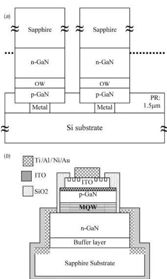
low-pressure metal-organic chemical vapor deposition (MOCVD) system (Emcore D80). These LED structures (dominant wavelength at 470 nm) consisted of a 30 nm thick buffer layer, a 2 µm thick undoped GaN layer, a 3 µm thick Si-doped n-GaN layer, five periods of InGaN/GaN quantum-well active layer, a 0.2 µm thick Mg-doped p-AlGaN layer and an Mg-doped p+-GaN layer. In chip processing, the chip size was 180 × 180 µm2. The mesa size of 160 × 160 µm2 was defined by standard photolithography and partially etched using an inductively coupled plasma (ICP) etcher to expose an n-GaN layer for electrode formation. Then, an indium-tin-oxide (ITO) film was deposited on the p-GaN layer as the transparent and p-conductive layer by an electron-beam (E-beam) system in a 300◦C chamber. The textured ITO surface was fabricated using photolithographic and wet-etching HCl: H2O (5:1) solution to construct regular circular bowls of approximately 3–5 µm diameter and 2 µm space. The corresponding etching depth is around 60 nm to achieve a textured ITO surface for enhancing the light extraction [10,11]. The edge of the device was then further dry etched to the sapphire substrate for n-contact connection. A SiO2 (5000 ˚A) film was deposited on the surface and sidewall by an e-beam for passivation. Finally, Ti/Al/Ni/Au (5 nm/ 200 nm/400 nm/800 nm) were deposited on the n-GaN contact layer and p-electrode pad (90 µm diameter) on the ITO film. The sample was then subjected to an alloy process at 250◦C in a N2furnace for 20 min. In this way, a highly reflective mirror was formed on the structure sidewall. Then, the processed LED wafer was subjected to the laser scribe and broken into chips with dimensions of 180× 180 µm2. Then, these chips were separated by expanding facility and the chip space is 300 µm. The expanded chips were embedded in 1.5 µm thick photo resist and the schematic structure is shown in figure 1(a). After chips were transferred to a Si wafer, an ITO film was deposited on the backside and the sidewall of the sapphire substrate for conductive purposes. In other words, the ITO film deposited on the backside and sidewall of the sapphire will not only enhance the light extraction but also serve as an electrical connection between the n-GaN layer and the chip backside. After that, the expanded chips were transferred to tape again for removing the photo resist using organic solvent. Finally, single electrode pad GaN-based LEDs (SEP-LEDs) with small chip size were successfully fabricated and the schematic structure diagram is shown in figure1(b). The chips were then bonded on TO-46 with conductive silver-filled glue and without epoxy encapsulation for electrical and optical measurements.
3. Results and discussion
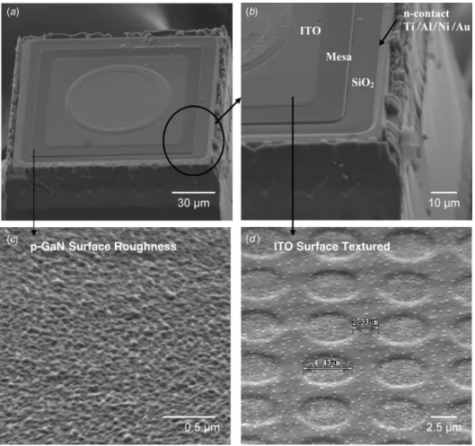
A scanning electron microscope (SEM) image of the chip profile is shown in figure 2(a). Obviously there is only one electrode pad on this device, which is different from conventional lateral GaN-based LEDs (CL-LEDs). The chip
(a)
(b)
Figure 1. Schematic structure diagrams of (a) p-side down
expanded chips embedded in PR; (b) single electrode pad GaN-based LED fabricated on a sapphire substrate.
and the mesa size are 180 × 180 and 160 × 160 µm2, respectively. Figure 2(b) describes the device structure. The surface roughness of the p-GaN and ITO layers is clearly shown in figures2(c) and (d). Both of the textured surfaces are useful to improve the light extraction efficiency by reducing the total internal reflective effect and increasing the probability of light escaping from semiconductor to air. For a detailed comparison of the electrical and optical characteristics, CL-LEDs of the same chip size (180 × 180 µm2) were also fabricated. Although these two types LEDs have the same chip size, the light emission areas of SEP-LEDs was still larger than those of CL-LEDs due to the reduction of the n-contact pad. A typical current versus voltage (I–V) curve is shown in figure 3(a). The forward voltages of SEP-LEDs and CL-LEDs at 20 mA current injection are about 3.15 and 3.35 V, respectively. The SEP-LEDs present a lower Vfthan that of CL-LEDs, indicating the lower series resistance and better current spreading properties of SEP-LEDs due to the special n-contact design. The n-contact area of SEP-LEDs not only circularly covered the chip edge but also covered the sidewall with the ITO film.
Figure 2. Scanning electron microscope (SEM) images of (a) chip profile, (b) detailed description, (c) top view of p-GaN surface roughness
and (d) surface texture of the ITO layer by photolithography and wet etching.
Current (mA) Voltage (V) Current (mA) Wall-Plug Efficiency (%) Power (mW) 0.0 0.5 1.0 1.5 2.0 2.5 3.0 3.5 4.0 0 10 20 30 40 50 60 SEP-LEDs CL-LEDs SEP-LEDs CL-LEDs SEP-LEDs CL-LEDs 0 2 4 6 8 10 12 14 16 18 20 0 5 10 15 20 25 30 35 40 45 50 55 60 0 2 4 6 8 10 12 14 (a) (b)
Figure 3. (a) Typical current versus voltage (I–V) characteristics of SEP-LEDs and CL-LEDs; (b) wall-plug efficiency and output power in
relation to the injection current of SEP-LEDs and CL-LEDs.
It is much more like a three-dimensional (3D) contact in comparison to the conventional two-dimensional (2D) contact. Figure3shows the output power and the wall-plug efficiency versus injection current for these two devices. It is clear that the light output power of the SEP-LEDs is higher than
the CL-LEDs. Under 20 mA current injection, it is found that the enhancement of light output power of the SEP-LEDs can be raised from 4.3 mW to 6.1 mW and the wall-plug efficiency exhibits 66.3% enhancement compared to the CL-LEDs. The results can be ascribed to the lower
Semicond. Sci. Technol. 23 (2008) 045013 Y C Lee et al
Intensity Intensity
(a) (b)
Figure 4. Optical and electro-luminescence (EL) microscope images of (a) SEP-LEDs and (b) CL-LEDs.
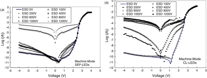
Voltage (V) -12 -11 -10 -9 -8 -7 -6 -5 -4 -3 -2 -1 0 -5 -4 -3 -2 -1 0 1 2 3 4 5 ESD 0V ESD 100V ESD 200V ESD 400V ESD 600V ESD 800V ESD 1000V ESD 1200V Log ( |A |) (a) Machine-Mode SEP-LEDs -12 -11 -10 -9 -8 -7 -6 -5 -4 -3 -2 -1 0 -5 -4 -3 -2 -1 0 1 2 3 4 5 ESD 0V ESD 100V ESD 200V ESD 400V ESD 600V ESD 800V ESD 1000V ESD 1200V Voltage (V) Log ( |A |) (b) Machine-Mode CL-LEDs
Figure 5. I–V characteristics as a function of a reverse pulse voltage in a machine-model ESD driving (a) SEP-LEDs and (b) CL-LEDs.
series resistance and the larger light emission area of SEP-LEDs. Optical and corresponding electro-luminescence (EL) microscope images (at 20 mA) of these two devices are shown in figures4(a) and (b). According to the EL intensity images, it is clearly observed that the SEP-LEDs present excellent current spreading characteristics. In contrast, a serious current crowding effect is observed between the shortest distance of the p- and n- contact pads of the CL-LEDs. The current crowding effect will affect device performances such as
reduced current injection efficiency, non-uniform lighting area, higher Joule heating, unstable reliability and device lifetime issues. In this study, the ESD resistance properties were measured by an Electro-Tech system simulator model 910. It could provide electrical pulses in the human body model and machine model. The machine model applied reverse pulse voltage from 0 V to −1200 V on these two types of devices. Figures5(a) and (b) show the I–V characteristics of the SEP-LEDs and the CL-LEDs after a reverse pulse voltage
injection. According to these figures, both leakage currents are less than 1 nA at−4 V before the ESD damage test. The curve of CL-LEDs shows a leakage current larger than 1 µA after the−200 V ESD test and a minimum occurred at 0 V after the−400 V ESD test. This minimum of the ohmic-like curve indicates that the p–n junction was short after−400 V reverse pulse voltage damage and the ESD resistance of the CL-LEDs is less than −400 V. Furthermore, the leakage current is, more seriously, accompanied by an increase of reverse pulse voltage. In contrast, it is clear that the SEP-LEDs exhibit higher ESD resistance (>−1000 V) than the CL-LEDs due to the uniform current spreading path and the lower series resistance.
4. Conclusion
In this paper, vertical structure and single electrode pad SEP-LEDs with a small chip size (180× 180 µm2) have been successfully fabricated on a sapphire substrate. There are various advantages in the novel SEP-LED chip, such as more light emitting area, lower series resistance, higher wall-plug efficiency, excellent current spreading and higher ESD resistance. This structure and fabricated method is more suitable for small chip size applications.
Acknowledgments
The authors would like to thank Dr S W Chiou of Huga Optotech Inc. for useful discussion and technical support.
This work was supported by the MOE ATU program and in part by the National Science Council of the Republic of China (ROC) in Taiwan under contract NSC95-2221-E009-235-MY3, NSC96-2628-E009-017-MY3, NSC96-2221-E009-094-MY3 and NSC96-2752-E009-007-PAE.
References
[1] Jiang H X, Jin S X, Li J, Shakya J and Lin J Y 2001 Appl. Phys. Lett.78 1303
[2] Nakamura S and Chichibu S F 2000 Introduction to Nitride Semiconductor Blue Laser Diode and Light Emitting Diodes (London: Taylor and Francis)
[3] Hirayama H 2005 J. Appl. Phys. 97 091101
[4] Wong W S, Sands T, Cheung N W, Kneissl M, Bour D P, Mei P, Romano L T and Johnson N M 2000 Appl. Phys. Lett.77 2822
[5] Peng W C and Wu Y C 2006 IEEE Photon. Technol. Lett.
18 613
[6] Lin W Y, Wuu D S, Pan K F, Huang S H, Lee C E, Wang W K, Hsu S C, Su Y Y, Huang S Y and Horng R H 2006 IEEE Photon. Technol. Lett.17 1809
[7] Shchekin O B, Epler J E, Trottier T A, Margalith T, Steigerwald D A, Holcomb M O, Martin P S and Krames M R 2006 Appl. Phys. Lett.89 1109
[8] Kim S J, Choi Y S, Han Y H, Kim C Y, Yu S J and Kim S G 2005 Phys. Status Solidi a 10 2034
[9] Kim S J 2005 IEEE Photon. Technol. Lett.17 1617
[10] Horng R H, Yang C C, Wu J Y, Huang S H, Lee C E and Wuu D S 2005 Appl. Phys. Lett.86 1101
[11] Pan S M, Tu R C, Fan Y M, Yeh R C and Hsu J T 2003 IEEE Photon. Technol. Lett.15 649