IEEE PHOTONICS TECHNOLOGY LETTERS, VOL. 21, NO. 13, JULY 1, 2009 899
The Ring-Shaped CMOS-Based Phototransistor With
High Responsivity for the UV/Blue Spectral Range
Yu-Wei Chang and Yang-Tung Huang, Member, IEEE
Abstract—The ring-shaped phototransistor with a floating
bulk enclosed by a ring-shaped photodiode is proposed to en-hance the responsivity for the ultraviolet/blue spectral range. The P-channel metal–oxide–semiconductor field-effect transistor and N-channel metal–oxide–semiconductor field-effect transistor phototransistors were manufactured using a standard 0.35- m complimentary metal–oxide–semiconductor (CMOS) technology. When the phototransistors were illuminated with 400-nm light, the measurement results for 3-V bias demonstrated a responsivity higher than 1500 A/W, which is also superior to that of other reported photodetectors manufactured using a standard CMOS technology. Even for very small bias voltages such as 0.1 V, the phototransistor can exhibit a responsivity of 17.9 A/W.
Index Terms—Optical receivers, optoelectronic devices,
pho-todetectors, phototransistors.
I. INTRODUCTION
T
HE development of a photodetector with high respon-sivity for the ultraviolet (UV)/blue spectral range has attracted much interest for many applications, such as ical analysis and optical storage systems [1]–[4]. For biochem-ical analysis, the detection of the optbiochem-ical properties changed by chemical reactions is a competent approach to examine various important biological molecules. Through the chemical reac-tions, the change of the emitted—or absorbed—light intensity is generally less than 1 W. Regarding the reported methods, the luminol H O HRP reaction involves the emission of 425-nm light [1], and the ABTS H O HRP reaction involves the absorption of 415-nm light [2]. For optical storage systems, an optical pickup unit detects the laser light (less than 1 W) re-flected from a storage disc and converts it into electrical output signals [3]. The recording density of the disc is determined by the minimum spot size that the laser light can be focused on, and the spot size is proportional to the laser wavelength. Therefore, a higher recording density can be obtained by using the laser of a shorter wavelength [4]. Compared with CD (780 nm) and DVD (650 nm), the Blu-ray Disc (405 nm) has a larger storage capacity and becomes a noticeable trend in the optical storage technology.Much work has been devoted to the realization of photode-tectors using a standard complimentary metal–oxide–semicon-ductor (CMOS) technology or CMOS-compatible technologies
Manuscript received December 05, 2008; revised March 20, 2009. First pub-lished April 17, 2009; current version pubpub-lished June 17, 2009.
The authors are with the Department of Electronics Engineering and Insti-tute of Electronics, National Chiao Tung University, Hsinchu City 300, Taiwan (e-mail: [email protected]).
Digital Object Identifier 10.1109/LPT.2009.2020176
Fig. 1. Top view, cross section, and equivalent symbol of the proposed (a) PMOS phototransistor and (b) NMOS phototransistor.
in the last decade [1]–[11]. This is owing to its low cost, high throughput, and the capability for integration with consequent circuits without any process modification. A conventional CMOS photodiode can easily be formed by utilizing an N P , P N , or N P junction, but the respon-sivity for the UV/blue spectral range is low (about 0.2 A/W) [12]. Circumventing this drawback, a phototransistor can have a current amplification under moderate bias through the internal transistor action [13]. However, little work has been conducted on the phototransistor manufactured using a standard CMOS technology for the UV/blue spectral range.
In this research, the CMOS phototransistor was designed, fab-ricated, and measured. It exhibited an enhanced responsivity for the UV/blue spectral range.
II. DEVICESTRUCTURE ANDOPERATINGPRINCIPLE
The device structures of the proposed P-channel metal–oxide–semiconductor field-effect transistor (PMOS) and N-channel metal–oxide–semiconductor field-effect transistor (NMOS) phototransistor based on CMOS technology are shown in Fig. 1(a) and (b), respectively. For the PMOS phototransistor, the P source is placed in the center with the
900 IEEE PHOTONICS TECHNOLOGY LETTERS, VOL. 21, NO. 13, JULY 1, 2009
ring-shaped poly-silicon gate and P drain, while the N bulk ( ) is enclosed by the P ring ( ). For the NMOS phototransistor, the N source is placed in the center with the ring-shaped poly-silicon gate and N drain, while the P bulk ( ) is enclosed by the ring ( ). In both cases, the phototransistor can be regarded as a metal–oxide–semicon-ductor field-effect transistor (MOSFET) with a photodiode connected across the bulk ( ) and the square ring ( ), as shown in Fig. 1.
Serving as an optical sensor, the phototransistor leaves the bulk floating and mainly uses the N P junction to sepa-rate photogenesepa-rated electron-hole pairs [8]. The photogenesepa-rated carriers drifting into the bulk would change the bulk potential, and thereby change the threshold voltage as well as the output drain current.
For the UV/blue incident light, most photogenerated carriers are very close to the surface (within 0.2 m). Using the proposed ring-shaped layout style, the near-surface depletion region of the outer N P ring-shaped photodiode is enlarged and superior to that of a conventional MOSFET with the same area, so as to cause a larger shift amount of the threshold voltage. Hence a larger photocurrent response could be expected.
Regarding the proposed phototransistors, the bulk is left floating, while the applied fixed ring-source voltage is negative for PMOS and is positive for NMOS. The bulk-ring voltage resulting from the illumination can be described by the transposed diode equation [13]
(1) where , , , and are the thermal voltage, the photocurrent of the bulk-ring diode, the saturation current of the bulk-ring diode, and the incident optical power density, respectively; is functions of material parameters, transistor bias voltages, and the depletion region area of the N P junctions. Thus the resulted bulk-source voltage can be ex-pressed as . For illuminated PMOS, is negative since its N bulk accumulates excess electrons; for illuminated NMOS, is positive since its P bulk accumu-lates excess holes.
The shift amount of the threshold voltage due to the bulk charge effect is given by [13]
(2) where , , , , and are the permittivity of silicon, the unit electric charge, the doping concentration of the bulk, the oxide capacitance per unit area, and the bulk Fermi level from the intrinsic Fermi level, respectively. When PMOS and NMOS phototransistors are illuminated, the absolute value of the threshold voltage will both become smaller.
The photocurrent response is the difference in the output drain current, which can be expressed as
(3) where and denote the output drain current of the photo-transistor with and without illumination, respectively. It implies
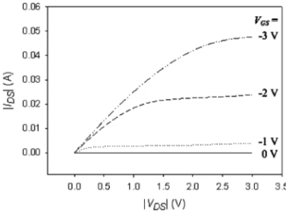
Fig. 2. MeasuredI–V characteristics of the PMOS phototransistor without il-lumination.
that of the phototransistor will increase with the N P sensing area , the channel aspect ratio , and the bias volt-ages and .
Overall, with advantages of the ring-shaped structure and the MOSFET amplification, the proposed CMOS phototransistor is expected to perform a better responsivity than conventional CMOS-based photodetectors.
III. EXPERIMENTALRESULTS
The proposed PMOS and NMOS phototransistors were re-spectively duplicated and concatenated to form each 10 10 array with a total area of 100 m 100 m, and they were manu-factured using the Taiwan Semiconductor Manufacturing Com-pany (TSMC) 0.35- m standard CMOS technology. To charac-terize these phototransistors, a UV/blue LED (Centenary 40327) with a peak of 400 nm was used as the light source, while its light intensity was adjusted by a power supply (Agilent E3631A). A reference photodetector and a pinhole were introduced to mea-sure the optical power density for various bias voltages applied to the LED. A precision semiconductor parameter analyzer (HP 4156A) and a test fixture (HP 16058A) were used to charac-terize the CMOS photodetectors.
Fig. 2 shows the measured current–voltage ( – ) characteris-tics of the PMOS phototransistor without illumination. The bias conditions were as follows: the source was grounded, the drain voltage swept from 0 to 3 V, the gate voltage stepped from 0 to 3 V, the bulk was floating, and the ring voltage was fixed at
3 V.
While the phototransistors were illuminated, the output drain current varied in response to the light intensity. For the PMOS phototransistor with V, the measured photocurrent responses are shown in Fig. 3(a). The larger the was, the larger the as well as the were. The photocurrent response divided by illumination intensity gives the DC responsivity, and the results are shown in Fig. 3(b). With V, the phototransistor exhibited a responsivity higher than 1500 A/W when the illumination intensity was less than 1 W, as the condition for applications in optical storage and most biochemical detection. This responsivity is 7500 folds higher than that of a conventional silicon P/N junction photo-diode (about 0.2 A/W) [12]. In addition, when the illumination
CHANG AND HUANG: RING-SHAPED CMOS-BASED PHOTOTRANSISTOR WITH HIGH RESPONSIVITY 901
Fig. 3. Optoelectronic characteristics of the PMOS phototransistor forV = 03 V with various V : (a) photocurrent response versus illumination intensi-ties and (b) DC responsivity versus illumination intensiintensi-ties.
TABLE I
UV/BLUERESPONSIVITY OF THECMOS PHOTODETECTORS
intensity was about 0.1 W, a higher responsivity of 7200 A/W can be achieved.
Even for very small bias voltages such as
V, the phototransistor can successfully detect the change of illumination intensity and exhibited a responsivity of about 17.9 A/W. The dark current was less than 1 nA.
Table I summarizes the measured responsivities for the PMOS and NMOS phototransistors under various bias con-ditions with illumination of 0.7- W 400-nm light. The characteristics of other reported photodetectors man-ufactured in a standard CMOS technology are also compared [9]–[11]. The difference between the PMOS and NMOS
pho-totransistor mainly results from that the N bulk of PMOS is distinguished from P , whereas the NMOS has a larger bulk region since P is inherently connected with P . For further applications in integrated circuits or sensor arrays, the floating P of NMOS phototransistor can be separated from the P by introducing a deep-N . Among these CMOS photodetectors, the proposed phototransistor exhibits a higher responsivity but at the expense of bandwidth. The measured dynamic responsivities for 1 Hz, 1 kHz, and 1 MHz were about 1700, 800, and 600 A/W, respectively. However, the bandwidth is sufficient for applications in biochemical analysis.
IV. CONCLUSION
In this letter, the ring-shaped phototransistor with a floating bulk enclosed by a ring-shaped photodiode based on CMOS technology is proposed for applications in the UV/blue spec-tral range with a high responsivity. Experimental results demon-strated that the responsivity for 400-nm light was higher than 1500 A/W, which is also superior to that of other reported pho-todetectors manufactured in a standard CMOS process. Even for very small bias voltages such as 0.1 V, the phototransistor can exhibit a responsivity of 17.9 A/W. The proposed device structure is therefore an attractive option in applications for the UV/blue spectral range.
REFERENCES
[1] U. Lu, B. C.-P. Hu, Y.-C. Shih, Y.-S. Yang, C.-Y. Wu, C.-J. Yuan, M.-D. Ker, T.-K. Wu, Y.-K Li, Y.-Z. Hsieh, W. Hsu, and C.-T. Lin, “CMOS chip as luminescent sensor for biochemical reactions,” IEEE Sensors J., vol. 3, no. 3, pp. 310–316, Jun. 2003.
[2] Y.-W. Chang, P.-C. Yu, Y.-T. Huang, and Y.-S. Yang, “A CMOS-com-patible optical biosensing system based on visible absorption spec-troscopy,” in IEEE Int. Conf. Electron Devices and Solid-State Circuits, 2007, vol. 2, pp. 1099–1102.
[3] J. Sturm, M. Leifhelm, H. Schatzmayr, S. Groiß, and H. Zimmermann, “Optical receiver IC for CD/DVD/blue-laser application,” IEEE J. Solid-State Circuits, vol. 40, no. 7, pp. 1406–1413, Jul. 2005. [4] A. Nemecek, G. Zach, R. Swoboda, K. Oberhauser, and H.
Zimmer-mann, “Integrated BiCMOS p-i-n photodetectors with high bandwidth and high responsivity,” IEEE J. Sel. Topics Quantum Electron., vol. 12, no. 6, pt. 2, pp. 1469–1475, Nov./Dec. 2006.
[5] W. Zhang, M. Chan, S. K. H. Fung, and P. K. Ko, “Performance of a CMOS compatible lateral bipolar photodetector on SOI substrate,” IEEE Electron Device Lett., vol. 19, no. 11, pp. 435–437, Nov. 1998. [6] M. A. Marwick and A. G. Andreou, “A UV photodetector with internal
gain fabricated in silicon on sapphire CMOS,” in IEEE Sensors Conf., 2007, pp. 535–538.
[7] W. Zhang and M. Chan, “A high gain n-well/gate tied PMOSFET image sensor fabricated from a standard CMOS process,” IEEE Trans. Electron Devices, vol. 48, no. 6, pp. 1097–1102, Jun. 2001.
[8] M. Schanz, W. Brockherde, R. Hauschild, B. J. Hosticka, and A. Te-uner, “CMOS photosensor arrays with on-chip signal processing,” in Proc. 23rd Eur. Solid-State Circuits Conf., 1997, pp. 236–239. [9] A. Ghazi, H. Zimmermann, and P. Seegebrecht, “CMOS photodiode
with enhanced responsivity for the UV/blue spectral range,” IEEE Trans. Electron Devices, vol. 49, no. 7, pp. 1124–1128, Jul. 2002. [10] A. Tibuzzi, G.-F. D. Bettaa, C. Piemontea, C. D. Natalea, A. D.
Am-icoa, and G. Soncinia, “High gain bipolar junction phototransistors with finger-shaped emitter for improved optical gas sensing in the blue spectral region,” Sens. Actuators A, Phys., vol. 136, pp. 588–596, 2007. [11] A. R. Pauchard, P.-A. Besse, and R. S. Popovic, “Dead space effect on the wavelength dependence of gain and noise in avalanche photo-diodes,” IEEE Trans. Electron Devices, vol. 47, no. 9, pp. 1685–1693, Sep. 2000.
[12] S. Donati, Photodetectors—Devices, Circuits, and Applications. En-glewood Cliffs, NJ: Prentice-Hall, 2000.
[13] S. M. Sze and K. K. Ng, Physics of Semiconductor Devices, 3rd ed. Hoboken, NJ: Wiley, 2007.