國 立 交 通 大 學
電 機 學 院 I C 設 計 產 業 研 發 碩 士 班
碩 士 論 文
Wimax 應用之快速傅立葉轉換軟硬體共同
設計
Trade-offs on Harware-Software Co-design
of FFT for Wimax applications
研 究 生:張登琦
指導教授:董蘭榮 教授
Wimax 應用之快速傅立葉轉換軟硬體共同
設計
Trade-offs on Hardware-Software Co-design
of FFT for Wimax applications
研 究 生:張 登 琦 Student:Teng-Chi Chang
指導教授:董 蘭 榮 Advisor:Lan-Rong Dung
國立交通大學
電機學院 IC 設計產業研發碩士班
碩 士 論 文
A ThesisSubmitted to College of Electrical and Computer Engineering National Chiao Tung University
in partial Fulfillment of the Requirements for the Degree of Master
in
Industrial Technology R & D Master Program on IC Design
January 2010
Hsinchu, Taiwan, Republic of China
Wimax 應用之快速傅立葉轉換軟硬體共同
設計
研究生:張 登 琦 指導教授:董 蘭 榮 博士國立交通大學電機學院產業研發碩士班
中文摘要
簡單的說,如果一個處理器有處理 1000 MIPS 的能力,則它願意提供多 少 MIPS 給快速傅立葉轉換運算,然後根據此 MIPS 去決定最適合此運算的 N 點分支傅立葉轉換硬體對於無線和行動通訊系統,傅立葉轉換模組是不可 或缺的部分,特別是當寬頻無線系統需要一個高速且低功率硬體於高速封包 式資料傳輸,這使得傅立葉轉換成為下一代無線系統必要的要求。在經過處 理器運算量分析後,N 點分支傅立葉轉換以硬體系統需要一個高速且低功率 硬體於高速封包式資料傳輸,這使得傅立葉轉換成為下一代無線系統必要的 需求。一般而言,傅立葉轉換模組的設計會針對特定的系統,因此,希望能 去設計一個可以適合不同標準規格的傅立葉轉換模組。在此論文中採用處理 器彈性的特色和硬體具有加速的機制去建立一個傅立葉轉換模組,並且可以 符合 IEEE 802.11n /16e 的規格要求。除此之外,我們提出對於單輸入輸出/ 多輸實現於系統中,並且它已 16 位元及 85MHz 產出率(Throughput rate)為規 格。之後,我們有針對是用於系統的傅立葉轉換架構做分析比較。最後,不 只有對 8 點分支傅立葉轉換於 FPGA 上做驗證,並且有針對提出的排程做驗 證是可以滿足 IEEE 802.11n/16e 的規格。Trade-offs on Hardware-Software Co-design of FFT for
Wimax applications
Student: Teng-Chi Chang Advisor: Dr. Lan-Rong Dung
Industrial Technology R & D Master Program of Electrical and Computer Engineering College
National Chiao-Tung University
Abstract
Briefly speaking, if a processor can process 1000 MIPS, it will provide which MIPS for us to operate Fast Fourier Transform (FFT). According to the MIPS it pro-vides us, we can decide which N-points branch FFT of ASIC is suitable for us. FFT module is an indispensable part for wireless and mobile communication, especially when broadband wireless systems require a high speed and low power hardware module for its packet-based high-speed data transfer. This has made the design of FFT processor a critical requirement for the next generation wireless systems. In general, FFT module is designed for specific system. Therefore, it is desirable to design adaptive FFT module for different standards. This thesis adopts processor flexible characteristic and ASIC accelerated mechanism to set up a flexible FFT module which can meet IEEE 802.11n/16e standards. Besides, we propose optimized timing schedule for SI-SO/MIMO systems. After processor computational analysis, 64-points branch FFT of ASIC can be applied in proposed system and it computes 16-bits input data at a throughput rate of 85MHz. After that, we compare various pipeline-based FFT archi-tectures suited to our system. Finally, it not only verifies the 8-points branch FFT on FPGA, but also checks proposed timing schedule which can satisfy IEEE 802.11n/16e specification.
誌 謝
首先感謝我的指導教授董蘭榮老師在我碩士班生涯的悉心指導,在於研究學 問的過程上讓我學會了更多以前沒碰過的觀念跟方向,也讓我學會解決問題的能 力與思考,處事態度上有所進步,在這段時間讓我受益良多。 同時也要感謝學長俊衛,再研究的時候給予的幫忙以及實驗室曾經一起奮鬥 相處的同學們志恆、建勛、宇佑、文俊、展嘉、嘉洋以及學弟建樺,謝謝你們熱 心的協助與指導。因為有你們的陪伴,使我的研究生活增添了許多歡樂愉悅,過 的非常充實。 最後要感謝我親愛的家人、及女友筱婷全家人,感謝他們的鼓勵、支持和愛 心以及一起經歷我求學生涯所有經過的大大小小事情,使我得以在精神與生活上 非常充實,順利完成學業。 僅以本論文獻給摯愛的大家、最深的謝意。 登琦 于新竹交大工程五館 2010年1月Contents
中文摘要 II
Abstract III
誌 謝 IV
Contents V
List of Figures ... VII List of Tables ... IX Chapter 1
Introduction ... 1
1.1 Motivation ... 1
1.2 Organization of this Thesis ... 2
Chapter 2 Backgroud ... 3
2.1 OFDM Backgrounds ... 3
2.2 WLAN MIMO-OFDM System ... 4
2.3 Flexible FFT Processor ... 6
2.4 Discrete Fourier Transform ... 7
2.4.1 Decimation-In-Time FFT Algorithm ... 8
2.4.2 Decimation-In-Frequency FFT Algorithm ... 9
2.5 Variable Length of FFT Architectures... 11
2.5.1 Memory-Based FFT Architectures ... 12
2.5.2 Pipeline-Based FFT Architectures ... 13
Chapter 3 Co-Design Analysis on ASIC and Processor of FFT ... 15
3.1 Introduction ... 15
3.3 FFT Computational Complexity Analysis ... 19
3.4 ASIC and Processor Timing Schedule Analysis ... 24
3.4.1 SISO System Timing ScheduleⅠ ... 25
3.4.2 SISO System Timing ScheduleⅡ ... 26
3.4.3 MIMO System Timing Schedule ... 28
3.5 ASIC and Processor Performance Estimation ... 31
3.5.1 SISO Ⅰ System Operation Comparison ... 33
3.5.2 SISO Ⅱ System Operation Comparison ... 37
3.5.3 MIMO System Operation Comparison ... 40
Chapter 4 Implementation of the Structure with MicroBlaze Processor ... 47
4.1 Introduction of the MicroBlaze Processor ... 47
4.2 Implementation of the Variable-Length FFT ... 48
4.2.1 Software Design on MicroBlaze Processor ... 49
4.2.2 Hardware Design on ASIC FFT ... 51
4.2.3 Integrate the Embedded System ... 54
4.3 MIPS of the Variable-Length FFT Implemented by MicroBlaze Processor ... 58
4.4 Error Analysis ... 61
Chapter 5 Conclusion ... 64
5.1 Conclusion ... 64
5.2 Work of Implementation Environment ... 65
List of Figures
Fig. 2.1 Traditional bandwidth allocation of a frequency multiplexing system .... 3
Fig. 2.2 Bandwidth allocation of OFDM ... 4
Fig. 2.3 Block diagram of IEEE 802.11n WLAN 2x2 transmitter system ... 5
Fig. 2.4 Block diagram of IEEE 802.11n WLAN 2x2 receiver system ... 5
Fig. 2.5 8-points radix-2 DIT FFT signal flow graph ... 9
Fig. 2.6 The butterfly signal flow graph of radix-2 DIF FFT ... 10
Fig. 2.7 8-points radix-2 DIF FFT signal flow graph ... 10
Fig. 2.8 Memory-based architecture block diagram ... 12
Fig. 2.9 Projection mapping of radix-2 DIF FFT signal flow graph ... 13
Fig. 3.1 Complexity comparison of Table 3.3 ... 18
Fig. 3.2 8-points radix-2 DIT FFT signal flow graph ... 19
Fig. 3.3 Radix-2 DIF FFT signal flow graph of a 16-points FFT ... 19
Fig. 3.4 Different cases of length FFT according to processor operations ... 24
Fig. 3.5 Time schedule Ⅰof SISO system ... 25
Fig. 3.6 SISO system block diagram of time scheduleⅠ ... 26
Fig. 3.7 Time scheduleⅡ of SISO system ... 27
Fig. 3.8 SISO system block diagram of time scheduleⅡ ... 27
Fig. 3.9 Time schedule of MIMO system ... 29
Fig. 3.10 MIMO system block diagram ... 30
Fig. 3.11 ASIC throughput analysis. ... 32
Fig. 3.12 64-points FFT operation comparison of time scheduleⅠ ... 33
Fig. 3.13 128-points FFT operation comparison of time scheduleⅠ ... 34
Fig. 3.14 512-points FFT operation comparison of time scheduleⅠ ... 34
Fig. 3.15 1024-points FFT operation comparison of time scheduleⅠ ... 35
Fig. 3.17 64-points FFT operation comparison of time scheduleⅡ ... 37
Fig. 3.18 128-points FFT operation comparison of time scheduleⅡ ... 38
Fig. 3.19 512-points FFT operation comparison of time scheduleⅡ. ... 38
Fig. 3.20 1024-points FFT operation comparison of time scheduleⅡ ... 39
Fig. 3.21 2048-points FFT operation comparison of time scheduleⅡ ... 40
Fig. 3.22 64-points FFT operation comparison of MIMO time schedule ... 41
Fig. 3.23 128-points FFT operation comparison of MIMO time schedule ... 42
Fig. 3.24 512-points FFT operation comparison of MIMO time schedule ... 43
Fig. 3.25 1024-points FFT operation comparison of MIMO time schedule ... 44
Fig. 3.26 2048-points FFT operation comparison of MIMO time schedule ... 45
Fig. 4.1 MicroBlaze core block diagram ... 47
Fig. 4.2 Separate the implementation of 64-points FFT for two parts ... 49
Fig. 4.3 Structure of MicroBlaze Processor’s programming diagram ... 50
Fig. 4.4 The butterfly signal flow graph of the radix-23 Fig. 4.5 Implementation hardware of multiplication with DIT FFT algorithm ... 51
2 2 ... 52
Fig. 4.6 Complex multiplier with four real multiplications and two real additions ... 53
Fig. 4.7 Integrate the embedded system design diagram ... 54
Fig. 4.8 The block of Dual-Port RAM (SRAM) ... 55
Fig. 4.9 Control Register ... 56
Fig. 4.10 State Machine ... 57
Fig. 4.11 Simulation of hardware operation ... 58
Fig. 4.12 Processor’s instructions analysis of scheduleⅠin SISO system ... 60
Fig. 4.13 Processor’s instructions analysis of scheduleⅡ in SISO system ... 60
Fig. 4.14 Processor’s instructions analysis in MIMO system ... 61
Fig. 4.16 The compare with output data ... 63
List of Tables
Table 2.1 Comparison of the hardware complexity of the receiver ... 6Table 2.2 FFT sizes and sampling rates needed in various communication sys-tems ... 7
Table 2.3 Comparisons of FFT architectures ... 11
Table 3.1 Multiplication comparison ... 16
Table 3.2 Multiplications and additions comparison ... 17
Table 3.3 Equation of multiplications and additions comparison ... 17
Table 3.4 Comparison operations of FFT size in IEEE 802.11n/16e standards .. 21
Table 3.5 Comparison of different length ASIC operations of a 64-points FFT . 22 Table 3.6 Comparison of different length ASIC operations of a 2048-points FFT ... 23
Table 3.7 Approximately calculation of latency cycles ... 31
Chapter 1
Introduction
1.1 Motivation
In digital signal processing and communications, FFT is one of the most utilized oper-ations. The FFT plays an important role in modern communication systems, so its inverse transform-IFFT does. It is desired that FFT module can flexibly adjust FFT size to meet vari-ous standards. Generally speaking, FFT is designed for specific standards such as Ultra-Wide Band (UWB) system needs high throughput FFT module and Very High Data Rate DSL (VDSL) system required long length FFT computation. Therefore, it is difficult to design a FFT module which is suitable for any system specification.
For custom hardware that is often less cost-effective and flexible than general proces-sors. Therefore, the approaches of ASIC have been added to achieve the high performance on software or processors. In the thesis, we discuss the ASIC and processor characteristic to de-sign variable-length FFT modules. ASIC plays an accelerated role in the proposed system and it executes partial FFT algorithm. Processor can flexibly execute remaining FFT computation and it takes the performance of processor into consideration. Therefore, the proposed system can meet in different communication systems by reconfiguring processor computation.
1.2 Organization of this Thesis
In this thesis, the proposed FFT system can process on IEEE 802.11n/16e standards and it not only proposes optimized timing schedule, but also provides ASIC and processor analysis which are shown in the following chapters. The list of each chapter we write five chapters. Chapter 1 is our motivation. Chapter 2 reviews the background that we introduce the MIMO OFDM system standards, FFT algorithm and comparison of different radix algorithm. Then, variable-length FFT architectures are described. Chapter 3 presents the Co-design analysis. First, we analyze FFT computational complexity which can calculate processor per-formance. After that, the proposed timing schedule and architectures are combined for SI-SO/MIMO systems. Finally, we can analyze the relationship between ASIC and processor according to MOPS (Million Operations per Second). Chapter 4 shows the implementation of the structure with MicroBlaze Processor on FPGA tools. In the implementation domain of FFT processor, we chose the “MicroBlaze embedded system” which is implemented by FPGA tools. The MicroBlaze embedded soft core is a Reduced Instruction set Computer (RISC). In the environment, we will show the MIPS (Million Instructions per Second) of variable-length FFT based on IEEE 802.11n/16e standards. Chapter 5 is conclusion of this thesis.
Chapter 2
Backgroud
2.1 OFDM Backgrounds
In modern communication systems, the OFDM (Orthogonal Frequency Division Multiplexing) algorithm is effective in combating the problem of frequency-selective fading, inter-symbol interference (ISI), and inter-carrier interference (ICI). It is also efficient for wi-deband data transmission.
Bandwidth allocation of traditional frequency multiplexing is shown in Fig. 2.1. The conventional systems not only keep all sub-channels away from overlapping each other, but also allow some guard band bandwidth such that adjacent sub-channels will not introduce in-ter-channel interference (ICI). This allocation method is inefficient in bandwidth utilization. However, in Fig. 2.2, OFDM uses orthogonal carriers to modulate signal of sub-channels and eliminate ICI that allow sub-bands overlap.
Fig. 2.2 Bandwidth allocation of OFDM
2.2 WLAN MIMO-OFDM System
Orthogonal Frequency Division Multiplexing (OFDM) is widely applied in high-speed Wireless Local Area Network (WLAN) such as IEEE 802.11a/g/n, Hiperlan/2, Wireless Per-sonal Area Network (WPAN) and Ultra-Wide Band (UWB) system. OFDM is a special case of multi-carrier transmission, where a single data stream is transmitted over a number of low-er rate sub-carrilow-ers. OFDM can be seen as eithlow-er a modulation technique or a multiplexing technique. One of the main reasons to use OFDM is to increase the robustness against fre-quency selective fading or narrowband interference. To eliminate the banks of sub-carriers oscillators and coherent demodulators required by frequency division multiplex, Discrete Fourier Transform (DFT) processor is essential to be implemented.
Multiple-Input Multiple-Output (MIMO) system was instituted by Marconi in 1908. Channel fading can be suppressed by multiple antennas in both transmitter and receiver, called MIMO system, have received significant attention in recent years owing to their poten-tial to increase system capacity.
The High Throughput Task Group which establishes IEEE 802.11n standard is going to draw up the next-generation WLAN proposal based on the 802.11a/g which is the current OFDM-based WLAN standards [1]. The IEEE 802.11n standard based on the MIMO OFDM system provides very high data throughput rate from the original data rate 54 Mb/s to the data rate in excess of 600 Mb/s because the technique of the MIMO can increase the data rate by extending an OFDM-based system. A block diagram of the 2x2 transceiver and receiver of IEEE 802.11n is shown in Fig. 2.3 and Fig. 2.4. Depending on the desired data rate, the mod-ulation scheme can be Binary Phase Shift Keying (BPSK), Quaternary Phase Shift Keying
(QPSK), or Quadrature Amplitude Modulation (QAM) with 1-6 bits. The encoding rates in this specification are 1/2, 2/3, 3/4, or 5/6. The number of spatial sequence is supported by 1, 2, 3, or 4. The guard interval period is 400 ns or 800 ns. The bandwidth of the transmitted signal is 20 or 40 MHz. The FFT (Fast Fourier Transform) size is 64 points or 128 points based on IEEE 802.11n standard.
FEC encorder
Puncture Parser
Interleaver QAM mapping Insert pilot IFFT
Interleaver QAM mapping Insert pilot IFFT
Insert GI PreambleInsert
Surfix
windowing Analog & RF
Insert GI PreambleInsert
Surfix
windowing Analog & RF
Fig. 2.3 Block diagram of IEEE 802.11n WLAN 2x2 transmitter system
Packet Detection
Coarse Freqsyn
Symboltiming
Fine Freqsyn
Remove Guard Interval
FFT Channel Estimation Phase Tracking Equalizer Soft Bit Demapper Deinterleaver Soft Bit Demapper Deinterleaver Deparser Depunture Viterbi Decoder
Fig. 2.4 Block diagram of IEEE 802.11n WLAN 2x2 receiver system
complexities greatly compared with the current WLAN standards. The FFT/IFFT processor is one of the highest computational complexity modules in the physical layer of the IEEE 802.11n standard, as shown in Table 2.1 [2]. Multiple FFT processors are added to deal with multiple data sequences in a MIMO OFDM system. Therefore, FFT causes a large increase in the hardware complexity and power consumption.
Table 2.1 Comparison of the hardware complexity of the receiver Multiplier Adder Register Gate Count
(K) Packet Detection 4 4 50 50 AGC 1 1 1 30 Frequency Offset 4 18 96 80 Frame Detection 8 8 8 50 FFT 1 12 68 160 Channel Estima-tion 0 0 128 60
2.3 Flexible FFT Processor
OFDM technique plays an important role in wireless and modern communication sys-tems. The FFT processor is one of the highest computational complexity modules and FFT sizes, sampling rates are different in various standard requirements that Table 2.2 shows. It is desired to design a single FFT processor which adapts to various FFT sizes for different communication standards.
Table 2.2 FFT sizes and sampling rates needed in various communication systems Communication
Sys-tem
FFT Size (Sampling Rate)
802.11a 64 (20MHz) 802.11n 64 (20MHz)、128 (40MHz) 802.16e 2048 (20MHz)、1024 (10MHz)、512 (5MHz)、 128 (1.25MHz) DAB 2048、1024、512、256 (2MHz) DVB-T 8192、2048 (8MHz) DVB-H 4096 (8MHz) ADSL 512 (2.2MHz) VDSL 8192 (34.5MHz)、4096 (17.3MHz)、2048 (8.6MHz)、1024 (4.3MHz)、512 (2.2MHz) UWB 128 (528MHz)
2.4 Discrete Fourier Transform
The basic N-point DFT (Discrete Fourier Transform) X(k) of a complex data se-quence x(n) is defined as:
} 1 ..., , 1 , 0 { , ) ( ) ( 1 0 − ∈ =
∑
− = N k W n x k X N n nk N (1)Where the twiddle factor is
) 2 ( N nk j nk N
e
W
π −=
(2) Most approaches to improve the efficiency of the computation of the DFT exploit the symmetry and periodicity properties of the twiddle factor. First, the complex conjunctionsymmetry is * ) ( ) (
W
W
W
knN kn N n N k N = = − − (3) Second, the periodicity in n and k is
W
W
W
k N n N N n k N kn N ) ( ) ( + + = = (4) According to equation (1), the computational complexity is O (N2) through directly performing the required computation. It needs N2 complex multiplications and N (N-1) com-plex additions. To use the FFT algorithm, the computational comcom-plexity can be reduced to O (NlogrN), where r means the radix-r FFT. The radix-r FFT can be derived from DFT by decomposing the N-point DFT into a set of recursively related r-point transform. There are two types of FFT algorithm are Decimation-in-Time (DIT) and Decimation-in-Frequency (DIF) FFTs. The computational complexity of these two types is the same.2.4.1 Decimation-In-Time FFT Algorithm
The DIT algorithm is to decompose x(n) into radix-r module sequence (It is the same as DIT FFT Radix-2 algorithm).
∑
∑
∑
∑
∑
∑
∑
− = − = − = + − = − = + + = + + = + = = 1 2 / 0 2 / 1 2 / 0 2 / 1 2 / 0 ) 1 2 ( 1 2 / 0 2 1 0 ) 1 2 ( ) 2 ( ) 1 2 ( ) 2 ( ) ( ) ( ) ( ) ( N r rk N k N N r rk N N r k r N N r rk N odd n kn N even n kn N N n nk N W r x W W r x W r x W r x W n x W n x W n x k X : : (5)Fig. 2.5 shows an example of the 8-points DIT FFT radix-2 algorithm according to equation (5). We can find that order of the input time coefficients is must bit-reversed first in Fig. 2.5.
+ + + + + + - x w1 4 + -+ -+ -+ -x[0] x[4] x[2] x[6] x[1] x[5] x[3] x[7] X[0] X[1] X[2] X[3] X[4] X[5] X[6] X[7] x w0 8 -x w2 8 -+ + x w1 8 -x w3 8 -x w0 4 -x w0 4 -- x w1 4
Fig. 2.5 8-points radix-2 DIT FFT signal flow graph
2.4.2 Decimation-In-Frequency FFT Algorithm
The DIF algorithm is to decompose X(k) in the same way [3] (It is the same as DIF FFT Radix-2 algorithm).
{
}
∑
∑
∑
∑
∑
∑
∑
∑
∑
∑
∑
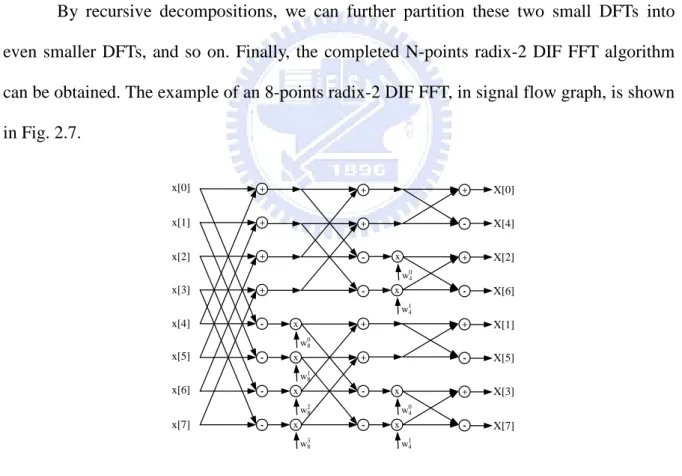
− = − = + − = + − = + − = − = + − = − = − = − = − = − + = − + = + = + + + = + + = + = − ∈ = − ∈ = 1 2 / 0 2 / 1 2 / 0 ) 1 2 ( 1 2 / ) 1 2 ( 1 2 / 0 ) 1 2 ( 1 2 / 0 2 / 1 2 / 0 ) 2 ( 2 1 2 / 0 2 1 2 / 2 1 2 / 0 2 1 0 2 1 0 ) 2 ( ) ( ) 2 ( ) ( ) ( ) ( ) 1 2 ( ) 2 ( ) ( ) 2 ( ) ( ) ( ) ( 1 ..., , 1 , 0 , ) ( ) 2 ( } 1 ..., , 1 , 0 { , ) ( ) ( N n n N nr N N n r n N N N n r n N N n r n N N n nr N N n r N n N N n nr N N N n nr N N n nr N N n nr N N n nk N W W N n x n x W N n x n x W n x W n x r X term odd W N n x n x W N n x W n x W n x W n x N r W n x r X term even N k W n x k X : : (6) As equation (6) shown, two (N/2)-points DFTs are composed of X (2r) and X (2r+1).It is well known that can combine these two equations as one basic butterfly (BF) module as shown in Fig. 2.6, where x(n) and x(n+N/2) are the input data.
+ - x wNn
x[n]+x[n+N/2]
x[n+N/2]
x[n]
{x[n]-x[n+N/2]}
w
NnFig. 2.6 The butterfly signal flow graph of radix-2 DIF FFT
By recursive decompositions, we can further partition these two small DFTs into even smaller DFTs, and so on. Finally, the completed N-points radix-2 DIF FFT algorithm can be obtained. The example of an 8-points radix-2 DIF FFT, in signal flow graph, is shown in Fig. 2.7. + + + + -+ + -+ + -+ -+ -+ -+ -x[0] x[1] x[2] x[3] x[4] x[5] x[6] x[7] X[0] X[4] X[2] X[6] X[1] X[5] X[3] X[7] x w0 8 x w18 x w2 8 x w3 8 x w04 x w1 4 x w0 4 x w1 4
Fig. 2.7 8-points radix-2 DIF FFT signal flow graph
2.5 Variable Length of FFT Architectures
FFT algorithms decompose the fundamental calculation of the DFT with a sequence of length N into continuously smaller subsequences. In section 2.4, the FFT algorithm is ap-plied not only in DSP, image processing and digital data transmission systems, but also in biomedical electronic engineering and home networking. Therefore, FFT processor has va-riable transform length in different systems. To be able to compute vava-riable FFT length, de-signer must to implement FFT processor with variable length.
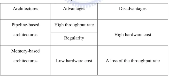
Generally speaking, FFT processor architectures can be divided into two types. One is pipeline-based architecture [4], [5], [6], [7], [8], [9], [10], and the other is memory-based ar-chitecture [11], [12], [13], [14], [15], [16], [17]. Different arar-chitectures for FFT processors have different advantages and disadvantages, as listed in Table 2.3. There are advantages and disadvantages between these two architectures.
Table 2.3 Comparisons of FFT architectures.
Architectures Advantages Disadvantages
Pipeline-based architectures
High throughput rate
High hardware cost Regularity
Memory-based
2.5.1 Memory-Based FFT Architectures
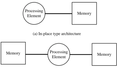
A general memory-based FFT processor structure mainly consists of a butterfly processing element (PE), a main memory, ROM for twiddle factor storage, and a controller. The butterfly PE is responsible for the butterfly operations required by FFT operations. Moreover, the architecture design of PE is dependent on the use of FFT algorithm and gener-ally dominates the performance of whole processor. The main memory stores processed data. The controller contains three functional units: data memory address generator, coefficient in-dex generator, and operation state controller. The data memory address generator follows a regular pattern to generate several addresses, and then the main memory provides input data for butterfly PE and stores output data from butterfly PE according to these addresses. The coefficient index generator provides indices to select coefficients form coefficient ROM or maps to coefficients through twiddle factor generator [18], [19].
Memory-based FFT architectures are designed to increase the utilization rate of but-terfly PE’s. Different from the pipeline-based architectures, memory-based FFT processor of-ten has one or two large memory block(s) that is accessed by all other PE components, instead of being distributed to many pipelined local arithmetic units.
Processing
Element Memory
Processing
Element Memory
Memory
(a) In-place type architecture
(b) Out-of-place type architecture
Main memory allocation and access strategy of a memory-based FFT processor can be classified as two types: in-place type and out-of place type [20], [21], [22]. In Fig. 2.8(a), in-place architecture, output data of butterfly PE are written back to the original memory bank with the same addresses as the previously loaded of input data [23]. Alternatively, if output data are written to another memory block without overwriting input data, this design will be generally called out-of-place Fig. 2.8(b). Therefore, memory size of the out-of-place design generally will be twice that of the in-place design.
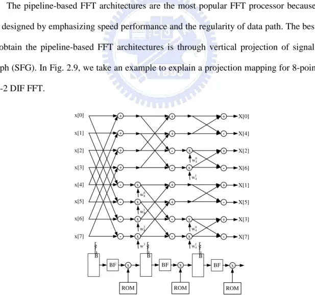
2.5.2 Pipeline-Based FFT Architectures
The pipeline-based FFT architectures are the most popular FFT processor because they are designed by emphasizing speed performance and the regularity of data path. The best way to obtain the pipeline-based FFT architectures is through vertical projection of signal flow graph (SFG). In Fig. 2.9, we take an example to explain a projection mapping for 8-points ra-dix-2 DIF FFT. + + + + -+ + -+ + -+ -+ -+ -+ -x[0] x[1] x[2] x[3] x[4] x[5] x[6] x[7] X[0] X[4] X[2] X[6] X[1] X[5] X[3] X[7] x w0 8 x w1 8 x w28 x w3 x w0 4 x w14 x w04 x w1 4 B u ff er BF x ROM B u ff er BF x ROM B u ff er BF x ROM
In Fig. 2.9, the structure of each stage obtained from the projection mapping is called the processing element (PE). A processing element contains a basic butterfly (BF) unit for addition and subtraction between two input data of each stage, a complex multiplier and a block of buffer are used to store and reorder data for the butterfly unit of next stage.
As the following paragraph that complexity comparison, FFT computational com-plexity analysis and time schedules will be discussed. SISOⅠ, SISOⅡ and MIMO sche-dules are the three time schesche-dules we will show in Chapter 3.
Chapter 3
Co-Design Analysis
on ASIC and Processor of FFT
3.1
Introduction
In recent years, a lot of products with some digital signal processing (DSP) techniques have become very popular. They are often more cost-effective and less risky than custom hardware, particularly for low-volume applications, where the development cost of custom ICs may be prohibitive.
In a MIMO OFDM system [24], multiple antennas need multiple FFT and inverse transform (IFFT) processors in transmitter and receiver shown in Fig. 2.3 and Fig. 2.4. Thus, it causes a large increase in the hardware complexity and power consumption. Besides, based on various standards, designers need to re-design different length and throughput of FFT pro-cessors that shown in Table 2.2. In recent years, applications in processor become very popu-lar. We use the advantages of processor to propose a new method that the processor and ASIC co-design can enhance flexibility and utilize time schedule efficiently to reduce ASIC cost. We provide designers two crucial messages. How many processor’s performance needed in various environments? How many branch FFT need to be implemented by hardware in vari-ous processors?
3.2
Complexity Comparison
From Table 3.1 [25] and Table 3.2 [26] show the multiplication and additions compar-ison, the multiplication and addition of radix-8 have the lowest complexity compared with radix-2 and radix-4. In Table 3.1, the constant multiplication can be implemented by shifters and adders, which the hardware cost is smaller than a real multiplication. Table 3.3 [27] is the complexity equation of multiplications and additions that the radix-8 type-1 algorithm is the original radix-8 FFT algorithm. In radix-8 type-2 algorithm, we replace multiplication of 1
8
W
into p additions that the 1 8
W will be implemented in the next section 4.4.2: “Hardware De-sign on ASIC FFT”.
Table 3.1 Multiplication comparison [25] N-point Radix-2 Radix-4 Radix-8
Multiplier Multiplier Multiplier Multiplier Constant Multiplier
8 2 3 0 2 16 10 8 6 4 32 34 31 20 8 64 98 76 48 32 128 258 215 152 64 256 642 492 376 128 512 1538 1239 824 384 1024 3586 2732 2104 768 2048 8194 6487 4792 1536 4096 18434 13996 10168 4096 8192 40962 32087 23992 8192
Table 3.2 Multiplications and additions comparison [26] Real Multiplications Real Additions N-point All Used by Radix-2 All Used by Radix-4 All Used by Radix-8 All Used by Radix-2 All Used by Radix-4 All Used by Radix-8 16 24 20 152 148 32 88 408 64 264 208 204 1032 976 972 128 720 2054 256 1800 1392 5896 5488 512 4360 3204 13566 12420 1024 10248 7856 30728 28336
Table 3.3 Equation of multiplications and additions comparison[27] Algorithm Real Multiplication Real Addition
Radix-2 8 2 7 log 2 3 2N− N+ N 8 2 7 log 2 5 2N− N+ N Radix-4 log 3 3 8 9 2N− N+ N 3 3 log 8 25 2N− N+ N Radix-8 Type-1 4 ) 3 (log 24 25 2N− + N 4 8 25 log 24 73 2N− N+ N Radix-8 Type-2 4 8 25 log 24 21 2N− N+ N 4 8 25 log 24 73 8 2 − + + N N N p
According to the hardware area and power consumption of complex number multiplier, we only focus on the number of real number multiplications. In Fig. 3.1, radix-8 type-2 has the lowest computational complexity, so we choose radix-8 type-2 as the building block to implement FFT algorithm.
3.3
FFT Computational Complexity Analysis
As the equation (6) shown in section 2.4.2: “Decimation-In-Frequency FFT Algo-rithm” is composed by even term X(2r) and odd term X(2r + 1) of two (N/2)-point DFTs. It is well known that one can combine these two equations as one basic butterfly (BF) module as shown in Fig. 3.2, where x(n) and x(n+N/2) are the input data.
+ - x wNn
x[n]+x[n+N/2]
x[n+N/2]
x[n]
{x[n]-x[n+N/2]}
w
NnFig. 3.2 The butterfly signal flow graph of radix-2 DIF FFT
By recursive decompositions, we can further partition small DFTs into even smaller DFTs, and so on. For example, an 8-points radix-2 DIF FFT, in signal flow graph, is shown in Fig. 3.3. + + + + + + - x w1 4 + -+ -+ -+ -x[0] x[4] x[2] x[6] x[1] x[5] x[3] x[7] X[0] X[1] X[2] X[3] X[4] X[5] X[6] X[7] x w0 8 -x w2 8 -+ + x w1 8 -x w3 8 -x w0 4 -x w0 4 -- x w1 4
Long-length FFT can be decomposed into several branch FFT by different radix algo-rithm. Take section 3.2: “Complexity Comparison” as a conclusion that radix-8 FFT reduces the complexity more than other radix. But FFT length is restricted to power of eight only. In any event, FFT architecture is composed of many butterfly units, and additions and multipli-cations form butterfly units. Thus, we can analyze FFT computation by calculating number of additions and multiplications.
Complex addition can be decomposed two real additions, and complex multiplication can be decomposed two real additions and four real multiplications as shown equation (1).
j )) N nk 2 cos( Im ) N nk 2 sin( (Re )) N nk 2 sin( Im ) N nk 2 cos( (Re ) j * ) N nk 2 sin( ) N nk 2 (cos( ) j Im* (Re ∗ π × + π × + π × − π × = π + π × + (1) Therefore, we try to evaluate different length of FFT computation complexity which is a little different from section 3.2: “Complexity Comparison”. Because we calculate any com-putation in terms of processor operations, it doesn’t include any hardware reduce comcom-putation, just like W81 can be implemented by shifters and adders. In this article, we take IEEE
802.11n/16e standards into consideration as shown in Table 2.2 of section 2.3: “Flexible FFT Processor”. FFT length covers from 64-points to 2048-points. We regard real addition or real multiplication as an operation in the analysis. In IEEE 802.11n/16e standards, 64-points/ 2048-points is the critical case separately, because of long-length FFT increase operations dramatically and symbol durations are the same shown in Table 3.4. Therefore, we analyze these two cases and assume partial branch FFT which is implemented by hardware as shown in Table 3.5 and Table 3.6. This analysis can be applied to others standards.
In Table 3.4, the processor operations are added by real additions and real multiplica-tions. According to equation (2), the processor operations are divided into three parts:
Addi-tion operaAddi-tions, multiplicaAddi-tions operaAddi-tions and operaAddi-tions for radix-8 only. AddiAddi-tion opera-tions present the all used addiopera-tions numbers of remaining FFT stages. Multipliers operaopera-tions are the all used multiplications numbers of remaining FFT stages. Operations for radix-8 only mean that because of the radix-8 FFT algorithm just only uses the W81 and W83 constants than other radix. Therefore, we must take the operations for radix-8 only when we use the ra-dix-8 FFT algorithm, the other radix will not be used. This analysis can be applied to others FFT sizes.
Table 3.4 Comparison operations of FFT size in IEEE 802.11n/16e standards 802.11n FFT Size(Sampling Rate) Processor Operations = Real additions
+Real multiplications
128 (40 MHz) 3142
64 (20 MHz) 1254
802.16e FFT Size(Sampling Rate) Operations = Real additions +Real multip-lications 2048 (20 MHz) 83462 1024 (10 MHz) 38150 512 (5 MHz) 16518 128 (1.25 MHz) 3142 } = = = = = + × × × + − × − × + × × = + + =
∏
∑ ∏
K {1,2,3, n , Rn -radix Rn groups, 8 -radix of Number K stages, remaining of Number S 1, R : where ) 4 (2 2 K 8 N )) 1 R ( ) 1 R N ( ) R ( ( S N 2 Operations Processor 0 1 j i 1 j stage 0 -i j 0 j addition operations for radix-8 only multipliers operations(2)
Table 3.5 is an example that shows all the remaining stages of the 64-points FFT pro-cessor operations according to equation (2). If we want to do a radix-8 of 64-points FFT, we can only choose one stage to perform. Therefore, we choose stage is 1 because we only do one time radix-8 through the remaining stages; S is 3 because radix-8 reduces 3 stages; N is 64 that is because we choose 64-points FFT to process; K is 1 because we choose radix-8 that we must consider the constants of W81 and W83. Finally, we can take 2*64*3+7*7*(2+4)+ 1*8*2*(2+4) = 774 which 774 is our desired processor operations. By the same way, Table 3.6 is the processor operations of 2048-points FFT according to equation (2).
Table 3.5 Comparison of different length ASIC operations of a 64-points FFT ASIC length of
64-points FFT
Operations = Real additions + Real multiplications
64 0 32 2*64+31*1*(2+4) = 314 16 2*64*2+15*3*(2+4) = 526 8 2*64*3+7*7*(2+4)+1*8*2*(2+4) = 774 4 2*64*4+31*1*(2+4)+2*3*7*(2+4)+ 1*8*2*(2+4) = 1046 2 2*64*5+15*3*(2+4)+4*1*7*(2+4)+ 1*8*2*(2+4) = 1174 0 2*64*6+7*7*(2+4)+8*0*7*(2+4)+2*8*2*(2+4) =1254
Table 3.6 Comparison of different length ASIC operations of a 2048-points FFT ASIC length of
2048-points FFT
Operations = Real additions + Real multiplications
2048 0 1024 2*2048+1023*(2+4) = 10234 512 2*2048*2+511*3*(2+4) = 17390 256 2*2048*3+255*7*(2+4)+256*2*(2+4) = 26070 128 2*2048*4+1023*(2+4)+2*127*7*(2+4)+256*2*(2+4) = 36262 64 74246-2*2048*6-32*7*7*(2+4)+1*256*2*(2+4) = 43334 32 2*2048*6+255*7*(2+4)+8*31*7*(2+4)+2*256*2*(2+4) = 51846 16 74246-2*2048*4+32*15*3*(2+4)-32*7*7*(2+4)+1*256*2*(2+4) = 60166 8 74246-2*2048*3+2*256*2*(2+4) = 68102 4 2*2048*9+255*7*(2+4)+8*31*7*(2+4)+8*8*3*7*(2+4)+ 3*256*2*(2+4) = 75270 2 74246-2*2048+256*1*3*(2+4)+2*256*2*(2+4) = 80902 0 2*2048*2+2*511*3+4*511*3+4*(10882+3332)+3*256*2*(2+4) = 83462
Not only 64-points/2048-points is the critical case in IEEE 802.11n/16e separately but also we will show the other cases, such as 128-points, 512-points, 1024-points FFT, as shown in Fig. 3.4.
In Fig. 3.4, the x-axis means which FFT length of ASIC we can choose; the y-axis is the processor operations we calculate from equation (2). Take an example of IEEE 802.16e 2048-points FFT from Fig. 3.4, if the processor only provides 30000 operations for us to do FFT, we will choose 256-points ASIC FFT for our branch FFT. It means the processor just
takes 26070 operations to do software FFT and then the other remaining stages will be processed by 256-points ASIC FFT. As the following paragraph, users can decide how much operations they want to provide for software to calculate FFT and then the others can be done for ASIC FFT by hardware. That is why we conclude the Fig. 3.4 of all these cases according to equation (2). 2 4 8 16 32 64 128 256 512 1024 2048 0 1 2 3 4 5 6 7 8 9x 10
4 Five kinds of Varible-Length FFT
FFT Length of ASIC N um ber of P roc es s or O per at ions 16e 2048-points FFT 16e 1024-points FFT 16e 512-points FFT 11n 128-points FFT 11n 64-points FFT
Fig. 3.4 Different cases of length FFT according to processor operations
3.4
ASIC and Processor Timing Schedule Analysis
In this article, because we need to design a variable-length FFT module in our system, timing schedules need to be executed independently. The goal is that we try to lower length of branch FFT and enhance processor and ASIC utilization.
3.4.1 SISO System Timing ScheduleⅠ
In SISO system we proposed two schedules. First in scheduleⅠ, we input sequences and write it into memory which can receive continuous data and reorder data. After that process data sequences have been ordered within symbol duration, therefore processor and ASIC utilization are not 100% as shown in Fig. 3.5. In other words, processor has less time to operate. Because of ASIC occupies part of symbol duration; therefore the processor needs better operations to performance.
Symbol Duration Symbol Duration Symbol Duration Symbol Duration Processor Process ASIC SRAM Read /Write Data Output Processor Process ASIC SRAM Read /Write Data Output Processor Process ASIC SRAM Read /Write Data Output Processor Process ASIC SRAM Read /Write Data Output
1
2
3
4
Fig. 3.5 Time schedule Ⅰof SISO system
In Fig. 3.6, it shows system block diagram based on time scheduleⅠ. This module is used to communicate On-Chip Peripheral Bus (OPB) handshake signals [28] between soft-ware and hardsoft-ware. Softsoft-ware is used to operate FFT softsoft-ware parts with C-language. ASIC FFT was responsible for branch FFT algorithm if the software parts have been prepared. Con-trol register and state machine modules are stored conCon-trol signals which govern entire data flow.
MicroBlaze Processor Software MUX Memory ASIC FFT Control Reg. State Machine A1 D1 A2 D2 A D Hardware 1 2 3 DOPB
Fig. 3.6 SISO system block diagram of time scheduleⅠ
In Fig. 3.6, it is the block diagram of SISOⅠ, which is designed according to Fig. 3.5 time schedule. In a symbol duration time, there are three steps must be process. First, step 1 is the software part, by reading/writing data between memory and software interface we can ac-complish the software part. Second, in order to do the ASIC N-points branch FFT, step 2 is an active signal to execute ASIC FFT that the signal is composed by control register and state machine. Third, step 3 is to do hardware N-points branch FFT. According to these three steps works in one symbol duration the time schedule Ⅰof Fig. 3.5 will be presented.
3.4.2 SISO System Timing ScheduleⅡ
Second, in schedule Ⅱ, it makes efforts to raise processor skill and ASIC utilization shown in Fig. 3.7. It not only decreases processor operations per second, but also can cut down the power consumption because of decreasing clock frequency. Additional buffer is
used to increase processor and ASIC processing time up to one symbol duration, but it causes more hardware cost shown in Fig. 3.8.
Symbol Duration Symbol Duration Symbol Duration Symbol Duration
Processor Process ASIC SRAM Read /Write Data Output Processor Process Processor Process Processor Process SRAM Read /Write SRAM Read /Write SRAM Read /Write SRAM Read /Write ASIC Data Output ASIC Data Output ASIC Data Output Processor Process
1
1
1
1
2
2
3
3
2
2
4
4
3
3
5
5
4
4
Fig. 3.7 Time scheduleⅡ of SISO system
MicroBlaze
Processor
Software
MUX
Memory2
ASIC
FFT
Control Reg. State Machine A1 D1 A2 D2 A2 D2Hardware
Memory1
A1 D11
2
3
4
DOPBIn Fig. 3.8, it is the block diagram of SISOⅡ, which is designed according to Fig. 3.7 time schedule. In two symbol duration time, there are four steps must be process. First, step 1 is the software part, by reading/writing data between memory 1 and software interface we can accomplish the software part. Step 2, we write the final data of software part to memory 2 be-cause the memory can be used by hardware independently. Third, in order to do the ASIC N-points branch FFT, step 3 is an active signal to execute ASIC FFT that the signal is com-posed by control register and state machine. Fourth, step 4 is to do hardware N-points branch FFT with memory 2 and when the hardware has work with memory 2, at the same time the processor can return back to memory 1 execute the next event of the next symbol. According to these fourth steps work, step 1 to step 3 works in first symbol duration and step 4 works in the next symbol duration. By several of continuous symbol durations, the time schedule Ⅱof Fig. 3.5 will be presented. In conclusion, the hardware N-points branch FFT is executed in the next symbol duration. Therefore, SISOⅡ not only decreases processor operations per second, but also can cut down the power consumption because of decreasing clock frequency than SISO Ⅰ.
3.4.3 MIMO System Timing Schedule
In general, channel fading can be suppressed by multiple antennas in both transmitter and receiver in MIMO system, but it also increases hardware area dramatically. Therefore, time schedule in MIMO system, it tries to minimize hardware area and enhance processor and ASIC utilization simultaneously. We find that time scheduleⅡ in SISO system which have many bubbles can be utilized to process others computation. Based on this concept, we pro-posed a suitable for MIMO system which can eliminate bubbles by processing another anten-na’s sequences which exchange processor and ASIC processing order as shown in Fig. 3.9.
Symbol Duration Processor Process ASIC SRAM Read /Write Data Output Processor Process SRAM Read /Write
1
11
11
11
21
21
1 ASIC Data Output1
21
2 Symbol Duration Processor Process ASIC SRAM Read /Write Data Output Processor Process SRAM Read /Write2
12
12
12
22
22
1 ASIC Data Output2
22
2 Symbol Duration Processor Process ASIC SRAM Read /Write Data Output Processor Process SRAM Read /Write3
13
13
13
23
23
1 ASIC Data Output3
23
2Fig. 3.9 Time schedule of MIMO system
ASIC and processor compute different antenna’s sequences by turns within half sym-bol duration. Therefore, comparison with SISO system, processor need two times operation performance per second in MIMO system. It can process two antenna’s sequences simulta-neously, and doesn’t need additional hardware of branch FFT shown in Fig. 3.10.
In Fig. 3.10, we present the MIMO system block diagram. There four memories for us to execute 2x2 antennas. We use eight steps to perform the MIMO system. First, in the first-half symbol, step 1 is used to operate software FFT of the first antenna and read-ing/writing data between memory 1 and software. Step 2, we write the final data of software part to memory 2 because the memory can be used by hardware independently. Third, in order to do the ASIC N-points branch FFT of the first antenna, Step 3 is an active signal to execute ASIC FFT that the signal is composed by control register and state machine. Fourth, step 4 is to do hardware N-points branch FFT with memory 2 and when the hardware has work with memory 2, at the same time the processor can change to memory 3 execute the second anten-na FFT of the second-half symbol. Fifth, in the second-half symbol, step 5 is used to operate software FFT of the second antenna and reading/writing data between memory 3 and software.
Step 6, we write the final data of software part to memory 4 because the memory can be used by hardware independently. Seventh, in order to do the ASIC N-points branch FFT of the second antenna, Step 7 is an active signal to execute ASIC FFT that the signal is composed by control register and state machine. Eighth, step 8 is to do hardware N-points branch FFT with memory 4 and when the hardware has work with memory 4, at the same time the processor can return back to memory 1 execute the first antenna FFT of the next symbol. In conclusion we perform the Fig. 3.10, step 1 to step 7 works in first symbol duration, which is divided two-half. Step 8 works in the next half symbol.
MicroBlaze
Processor
Software
MUX
Memory4
ASIC
FFT
Control Reg. State Machine A1 D1 A2 D2 A2 D2Memory3
A1 D11
2
3
4
Memory2
A2 D2Memory1
A1 D11
11
12
12
15
6
7
8
3.5
ASIC and Processor Performance Estimation
Since SISO schedules are proposed, an evaluation model is developed to verify speci-fication requirements. Bases on IEEE 802.11n/16e standards, we can introduce symbol period to calculate the performance of processor when different length of FFT is implemented by hardware. ASIC plays an accelerative role in the system. Increasing ASIC length of branch FFT can release load of processor. Not only 64-points/2048-points are the critical case in IEEE 802.11n/16e separately but also we will show the other cases, such as 128-points, 512-points, 1024-points FFT.
ScheduleⅠin SISO system, ASIC occupies some symbol duration shown in Fig. 3.5. Therefore, we need to calculate ASIC latency cycles approximately shown in Table 3.7 [29] and assume clock frequency is 50MHz for simulation, according to Fig. 3.4: “Number of Processor Operations”, we will show some cases of different length FFT shown in Fig. 3.11 ~ 3.15. In Table 3.7 we can make sure that the ASIC latency time can be included in a symbol duration time unit. When FFT length of ASIC is too short, it cannot gain any benefit to the processor. FFT length of ASIC affects operations of processor directly. More length branch FFT implemented by hardware will lower processor’s operations, but it increases cost.
Table 3.7 Approximately calculation of latency cycles
FFT Length Latency FFT Length Latency
0 0 64 103 2 2 128 208 4 4 256 336 8 8 512 592 16 26 1024 1616 32 44 2048 2640
Based on IEEE 802.11n/16e standards, the symbol duration of 64-points is 3.2µs and 2048-points is 102.5µs. In Table 3.7, the latency cycles of ASIC will be enough to be included in a symbol duration time unit, if the we choose 85 Mhz for out throughput rate at least. The throughput rate is shown in Fig. 3.11. It shows all the time schedules of N-points FFT based on IEEE standards, the throughput rate of 128-points is up to 85 Mhz at least. If we chose 85 Mhz for our throughput rate, we will know that this throughput rate it can be included in a symbol duration for all kinds of N-points branch FFT according to our time schedules, SI-SOⅠ, SISOⅡ and MIMO.
3.5.1 SISO Ⅰ System Operation Comparison
From Fig. 3.12 ~ 3.16, we can analyze the relationship between processor operations and branch FFT of ASIC. MOPS (Million Operations per Second) imply that processor operations divided by not needed symbol duration. When our system processes FFT algorithm only by processor, it shows that IEEE 802.11n need more operations per second. Therefore, we can calculate processor’s performance probably by MOPS. The time schedule diagram is based on Fig. 3.5. 2 4 8 16 32 64 0 100 200 300 400 500 600
compare 64-points SISO(I)
FFT Length of ASIC
M
OP
S
11n 64-points FFT(50Mhz)with radix-8 11n 64-points FFT(50Mhz)with radix-4 11n 64-points FFT(50Mhz)with radix-2
Fig. 3.12 64-points FFT operation comparison of time scheduleⅠ
In Fig. 3.12, it shows the 64-points FFT MOPS of radix-2, radix-4 and radix-8 based on IEEE 802.11n standard, x-axis is what kind of branch ASIC FFT we will decide, if the processor provide us some restricted MOPS to use shown on y-axis. Take an example, if the processor just only can provide us 300 MOPS, we will choose 8-points branch FFT as our ASIC because the two types of radix-4 and radix-8 algorithms are satisfy with the required MOPS (under 300 MOPS).In the other word, the radix-2 algorithm will be not satisfy the re-quired 300 MOPS (over 300 MOPS), if we choose 8-points branch FFT as our ASIC.
2 4 8 16 32 64 128 256 512 0 500 1000 1500 2000 2500
compare 128-points SISO(I)
FFT Length of ASIC
M
OP
S
11n 128-points FFT(50Mhz)with radix-8 11n 128-points FFT(50Mhz)with radix-4 11n 128-points FFT(50Mhz)with radix-2
Fig. 3.13 128-points FFT operation comparison of time scheduleⅠ
In Fig. 3.13, it shows the 128-points FFT MOPS of radix-2, radix-4 and radix-8 based on IEEE 802.11n standard, x-axis is what kind of branch ASIC FFT we will decide, if the processor provide us some restricted MOPS to use shown on y-axis. According to this figure, we can know that the radix-4 and radix-8 algorithms are more suitable than radix-2 algorithm because radix-2 algorithm will cost more MOPS then the other two types.
2 4 8 16 32 64 128 256 512 0 20 40 60 80 100 120 140 160 180 200
compare 512-points SISO(I)
FFT Length of ASIC
M
OP
S
16e 512-points FFT(50Mhz)with radix-8 16e 512-points FFT(50Mhz) with radix-4 16e 512-points FFT(50Mhz) with radix-2
In Fig. 3.14, it shows the 512-points FFT MOPS of radix-2, radix-4 and radix-8 based on IEEE 802.16e standard, x-axis is what kind of branch ASIC FFT we will decide, if the processor provide us some restricted MOPS to use shown on y-axis. According to this figure, we can know that the radix-4 and radix-8 algorithms are more suitable than radix-2 algorithm because radix-2 algorithm will cost more MOPS then the other two types.
2 4 8 16 32 64 128 256 512 1024 2048 0 50 100 150 200 250 300 350 400 450 500
compare 1024-points SISO(I)
FFT Length of ASIC
M
OP
S
16e 1024-points FFT(50Mhz)with radix-8 16e 1024-points FFT(50Mhz)with radix-4 16e 1024-points FFT(50Mhz)with radix-2
Fig. 3.15 1024-points FFT operation comparison of time scheduleⅠ
In Fig. 3.15, it shows the 1024-points FFT MOPS of radix-2, radix-4 and radix-8 based on IEEE 802.16e standard, x-axis is what kind of branch ASIC FFT we will decide, if the processor provide us some restricted MOPS to use shown on y-axis. According to this figure, we can know that the radix-4 and radix-8 algorithms are more suitable than radix-2 algorithm because radix-2 algorithm will cost more MOPS than the other two types.
2 4 8 16 32 64 128 256 512 1024 2048 0 200 400 600 800 1000 1200 1400
compare 2048-points SISO(I)
FFT Length of ASIC
M
OP
S
16e 2048-points FFT(50Mhz)with radix-8 16e 2048-points FFT(50Mhz) with radix-4 16e 2048-points FFT(50Mhz) with radix-2
Fig. 3.16 2048-points FFT operation comparison of time scheduleⅠ
In Fig. 3.16, it shows the 2048-points FFT MOPS of radix-2, radix-4 and radix-8 based on IEEE 802.16e standard, x-axis is what kind of branch ASIC FFT we will decide, if the processor provide us some restricted MOPS to use shown on y-axis. According to this figure, we can know that the radix-4 and radix-8 algorithms are more suitable than radix-2 algorithm because radix-2 algorithm will cost more MOPS then the other two types. In the other word, for N-points FFT we decide to implement, we can consider radix-8 and radix-2 algorithms first that the performance is better than only radix-2 algorithm.
In scheduleⅠof Fig. 3.12 ~ 3.16, user can design the system which we want. For ex-ample in IEEE 802.16e standard , if we want the processor used only for 700 MOPS, we will chose the “2048-points FFT operation comparison of time scheduleⅠ” method of Fig. 3.16, which we just use the 64-points ASIC FFT to design the system of this standard.
3.5.2 SISO Ⅱ
System Operation Comparison
ScheduleⅡ in SISO system shown in Fig. 3.17 ~ 3.21, it not only decreases processor op-erations per second than but also can cut down the power consumption. Therefore, the cost of MOPS in ScheduleⅡ is lese than scheduleⅠ. The time schedule diagram is based on Fig. 3.7.
2 4 8 16 32 64 0 50 100 150 200 250 300 350 400
compare 64-points SISO(II)
FFT Length of ASIC
M
OP
S
11n 64-points FFT(50Mhz)with radix-8 11n 64-points FFT(50Mhz)with radix-4 11n 64-points FFT(50Mhz)with radix-2
Fig. 3.17 64-points FFT operation comparison of time scheduleⅡ
In Fig. 3.17, it shows the 64-points FFT MOPS of radix-2, radix-4 and radix-8 based on IEEE 802.11n standard, x-axis is what kind of branch ASIC FFT we will decide, if the processor provide us some restricted MOPS to use shown on y-axis. This figure is designed according to time scheduleⅡ of SISOⅡ system. The performance is better than SISOⅠ sys-tem of Fig. 3.12. Take an example, if the processor provides us for 300 MOPS, we can choose the 4-points branch FFT of ASIC in SISO Ⅱ not the 8-points branch FFT of ASIC in SISOⅠ. Therefore, the cost of ASIC in SISO Ⅱ will be changed smaller than SISOⅠ, if the processor only provides 300 MOPS.
2 4 8 16 32 64 128 256 512 0 100 200 300 400 500 600 700 800 900 1000
compare 128-points SISO(II)
FFT Length of ASIC
M
OP
S
11n 128-points FFT(50Mhz)with radix-8 11n 128-points FFT(50Mhz)with radix-4 11n 128-points FFT(50Mhz)with radix-2
Fig. 3.18 128-points FFT operation comparison of time scheduleⅡ
In Fig. 3.18, it shows the 128-points FFT MOPS of radix-2, radix-4 and radix-8 based on IEEE 802.11n standard, x-axis is what kind of branch ASIC FFT we will decide, if the processor provide us some restricted MOPS to use shown on y-axis. This figure is designed according to time scheduleⅡ of SISOⅡ system. The performance is better than SISOⅠ sys-tem of Fig. 3.13. 2 4 8 16 32 64 128 256 512 0 20 40 60 80 100 120 140 160 180
compare 512-points SISO(II)
FFT Length of ASIC
M
OP
S
16e 512-points FFT(50Mhz)with radix-8 16e 512-points FFT(50Mhz) with radix-4 16e 512-points FFT(50Mhz) with radix-2
In Fig. 3.19, it shows the 512-points FFT MOPS of radix-2, radix-4 and radix-8 based on IEEE 802.16e standard, x-axis is what kind of branch ASIC FFT we will decide, if the processor provide us some restricted MOPS to use shown on y-axis. This figure is designed according to time scheduleⅡ of SISOⅡ system. The performance is better than SISOⅠ sys-tem of Fig. 3.14. 2 4 8 16 32 64 128 256 512 1024 2048 0 50 100 150 200 250 300 350 400
compare 1024-points SISO(II)
FFT Length of ASIC
M
OP
S
16e 1024-points FFT(50Mhz)with radix-8 16e 1024-points FFT(50Mhz)with radix-4 16e 1024-points FFT(50Mhz)with radix-2
Fig. 3.20 1024-points FFT operation comparison of time scheduleⅡ
In Fig. 3.20, it shows the 1024-points FFT MOPS of radix-2, radix-4 and radix-8 based on IEEE 802.16e standard, x-axis is what kind of branch ASIC FFT we will decide, if the processor provide us some restricted MOPS to use shown on y-axis. This figure is de-signed according to time scheduleⅡ of SISOⅡ system. The performance is better than SI-SOⅠ system of Fig. 3.15.
2 4 8 16 32 64 128 256 512 1024 2048 0 100 200 300 400 500 600 700 800 900
compare 2048-points SISO(II)
FFT Length of ASIC
M
OP
S
16e 2048-points FFT(50Mhz)with radix-8 16e 2048-points FFT(50Mhz) with radix-4 16e 2048-points FFT(50Mhz) with radix-2
Fig. 3.21 2048-points FFT operation comparison of time scheduleⅡ
In Fig. 3.21, it shows the 2048-points FFT MOPS of radix-2, radix-4 and radix-8 based on IEEE 802.16e standard, x-axis is what kind of branch ASIC FFT we will decide, if the processor provide us some restricted MOPS to use shown on y-axis. This figure is de-signed according to time scheduleⅡ of SISOⅡ system. The performance is better than SI-SOⅠ system of Fig. 3.16.
In “2048-points FFT operation comparison of time scheduleⅡ” method of Fig. 3.21 based on IEEE 802.16e standard, if we chose 64-points ASIC FFT, the processor operations will be used just only about 450 MOPS.
3.5.3 MIMO System Operation Comparison
Therefore, in MIMO system, processor and ASIC own half a symbol duration to com-plete operations. It can be expected that processor’s operations per second will be doubled of scheduleⅡ in SISO system as shown in Fig. 3.22 ~ 3.26 based on time schedule diagram
shown in Fig. 3.9. 2 4 8 16 32 64 0 100 200 300 400 500 600 700 800
compare 64-points MIMO
FFT Length of ASIC
M
OP
S
11n 64-points FFT(50Mhz)with radix-8 11n 64-points FFT(50Mhz)with radix-4 11n 64-points FFT(50Mhz)with radix-2
Fig. 3.22 64-points FFT operation comparison of MIMO time schedule
In Fig. 3.22, it shows the 64-points FFT MOPS of radix-2, radix-4 and radix-8 based on IEEE 802.11n standard, x-axis is what kind of branch ASIC FFT we will decide, if the processor provide us some restricted MOPS to use shown on y-axis. This figure is designed according to time schedule of MIMO system. The performance is twice than SISOⅡ system of Fig. 3.17, but the usage of time schedule in a symbol is improved. In a symbol duration, we can execute FFT two times and just only use one N-points branch FFT of ASIC well.
2 4 8 16 32 64 128 256 512 0 200 400 600 800 1000 1200 1400 1600 1800 2000
compare 128-points MIMO
FFT Length of ASIC
M
OP
S
11n 128-points FFT(50Mhz)with radix-8 11n 128-points FFT(50Mhz)with radix-4 11n 128-points FFT(50Mhz)with radix-2
Fig. 3.23 128-points FFT operation comparison of MIMO time schedule
In Fig. 3.23, it shows the 128-points FFT MOPS of radix-2, radix-4 and radix-8 based on IEEE 802.11n standard, x-axis is what kind of branch ASIC FFT we will decide, if the processor provide us some restricted MOPS to use shown on y-axis. This figure is designed according to time schedule of MIMO system. The performance is twice than SISOⅡ system of Fig. 3.18, but the usage of time schedule in a symbol is improved. In a symbol duration time unit, we can execute FFT two times and just only use one N-points branch FFT of ASIC well.
2 4 8 16 32 64 128 256 512 0 50 100 150 200 250 300 350
compare 512-points MIMO
FFT Length of ASIC
M
OP
S
16e 512-points FFT(50Mhz)with radix-8 16e 512-points FFT(50Mhz) with radix-4 16e 512-points FFT(50Mhz) with radix-2
Fig. 3.24 512-points FFT operation comparison of MIMO time schedule
In Fig. 3.24, it shows the 128-points FFT MOPS of radix-2, radix-4 and radix-8 based on IEEE 802.16e standard, x-axis is what kind of branch ASIC FFT we will decide, if the processor provide us some restricted MOPS to use shown on y-axis. This figure is designed according to time schedule of MIMO system. The performance is twice than SISOⅡ system of Fig. 3.19, but the usage of time schedule in a symbol is improved. In a symbol duration time unit, we can execute FFT two times and just only use one N-points branch FFT of ASIC well.
2 4 8 16 32 64 128 256 512 1024 2048 0 100 200 300 400 500 600 700 800
compare 1024-points MIMO
FFT Length of ASIC
M
OP
S
16e 1024-points FFT(50Mhz)with radix-8 16e 1024-points FFT(50Mhz)with radix-4 16e 1024-points FFT(50Mhz)with radix-2
Fig. 3.25 1024-points FFT operation comparison of MIMO time schedule
In Fig. 3.25, it shows the 1024-points FFT MOPS of radix-2, radix-4 and radix-8 based on IEEE 802.16e standard, x-axis is what kind of branch ASIC FFT we will decide, if the processor provide us some restricted MOPS to use shown on y-axis. This figure is de-signed according to time schedule of MIMO system. The performance is twice than SISOⅡ system of Fig. 3.20, but the usage of time schedule in a symbol is improved. In a symbol du-ration time unit of 2x2 antennas, we can execute FFT two times and just only use one N-points branch FFT of ASIC well.
2 4 8 16 32 64 128 256 512 1024 2048 0 200 400 600 800 1000 1200 1400 1600 1800
compare 2048-points MIMO
FFT Length of ASIC
M
OP
S
16e 2048-points FFT(50Mhz)with radix-8 16e 2048-points FFT(50Mhz) with radix-4 16e 2048-points FFT(50Mhz) with radix-2
Fig. 3.26 2048-points FFT operation comparison of MIMO time schedule
In Fig. 3.26, it shows the 2048-points FFT MOPS of radix-2, radix-4 and radix-8 based on IEEE 802.16e standard, x-axis is what kind of branch ASIC FFT we will decide, if the processor provide us some restricted MOPS to use shown on y-axis. This figure is de-signed according to time schedule of MIMO system. The performance is twice than SISOⅡ system of Fig. 3.21, but the usage of time schedule in a symbol is improved.
In the method of Fig. 3.26: 2048-points FFT operation comparison of MIMO time schedule. IEEE 802.16e standard, if we chose 64-points ASIC FFT, the processor operations will be used about 900 MOPS. In the other word, the MOPS of MIMO schedule will be doubled than the time scheduleⅡof SISOⅡ.
In this section, we introduce scheduleⅠ、Ⅱ in SISO system, and a schedule in MIMO system. According to time schedule system based on time scheduleⅠof SISOⅠand time scheduleⅡ of SISOⅡ, the cost of hardware in scheduleⅠis less than scheduleⅡ, but the uti-lization of scheduleⅠis less than scheduleⅡ. In MIMO system, bad utiuti-lization can be im-proved by changing ASIC and processor order. In 2x2 MIMO systems, it only needs a
pro-cessor and a branch FFT of ASIC. This schedule not only lower hardware cost, but also in-crease the utilization of module.
Therefore, we use the equation (2) to calculate the “Processor Operations” of 64-points, 128-points, 512-points,1024-points and 2048-points FFT and according to IEEE 802.11n/16e standards, we can predict the time of these three schedules (SISOI,SISOII and MIMO) in a symbol duration. Finally, MOPS (Million Operations per Second) has been eva-luated by our estimation. In next chapter, we want to implement the processor’s architecture of SISOⅠ in Fig. 3.6, SISOⅡ in Fig. 3.8 and MIMO in Fig. 3.10 with “Micro Blaze Proces-sor”, which is a embedded system implemented by FPGA tools
Chapter 4
Implementation of the Structure
with MicroBlaze Processor
4.1 Introduction of the MicroBlaze Processor
In the implementation domain of FFT processor, we chose the “MicroBlaze embedded system” which is implemented by FPGA tools. The MicroBlaze embedded soft core [30] is a reduced instruction set computer (RISC) optimized for implementation in Xilinx field pro-grammable gates arrays (FPGAs) [31]. Fig.4.1 is a block diagram depicting the MicroBlaze core. Program Counter Instruction counter Instruction Decoder Register File 32 x 32b Add/Sub Shift/Logical Multiply I-C ac h e Bus IF D -C ac h e Bus IF Instruction-side bus interface Data-side bus interface IOPB IXCL_M ILMB IXCL_S DXCL_M DXCL_S MFSL 0..7 SFSL 0..7 DOPB DLMB
Fig. 4.1 MicroBlaze core block diagram
From Fig. 4.1 that the MicroBlaze embedded soft core is highly configurable, allow-ing users to select a specific set of features required by their design. The processors features set includes the following. There are twenty-two 32-bits general purpose registers, 32-bits
![Table 3.1 Multiplication comparison [25]](https://thumb-ap.123doks.com/thumbv2/9libinfo/8004523.160155/26.892.189.744.518.1117/table-multiplication-comparison.webp)
![Table 3.2 Multiplications and additions comparison [26] Real Multiplications Real Additions N-point All Used by Radix-2 All Used by Radix-4 All Used by Radix-8 All Used by Radix-2 All Used by Radix-4 All Used by Radix-8 16 24 20 152 14](https://thumb-ap.123doks.com/thumbv2/9libinfo/8004523.160155/27.892.198.742.161.767/table-multiplications-additions-comparison-multiplications-additions-radix-radix.webp)