行政院國家科學委員會專題研究計畫 期中進度報告
介觀系統的自旋抽運與電荷抽運(1/3)
計畫類別: 個別型計畫 計畫編號: NSC93-2112-M-009-036- 執行期間: 93 年 08 月 01 日至 94 年 07 月 31 日 執行單位: 國立交通大學電子物理學系(所) 計畫主持人: 朱仲夏計畫參與人員: M. Buttiker, P. Samuelsson, A. G. Malshukov,唐志雄,鄔 其君,鍾淑維,王律堯,黃宇廷,簡靖航
報告類型: 精簡報告
報告附件: 出席國際會議研究心得報告及發表論文 處理方式: 本計畫可公開查詢
行政院國家科學委員會補助專題研究計畫
□ 成 果 報 告
□期中進度報告
介觀系統的自旋抽運與電荷抽運(1/3)
計畫類別:□ 個別型計畫 □ 整合型計畫
計畫編號:NSC 93 - 2112 - M - 009 - 036 -
執行期間: 2004 年 08 月 01 日至 2005 年 07 月 31 日
計畫主持人:朱仲夏 教授
共同主持人:
計畫參與人員:M. Buttiker, P. Samuelsson, Mal’shukov,唐志雄, 鄔
其君, 鍾淑維,王律堯,黃宇廷,簡靖航
成果報告類型(依經費核定清單規定繳交):□精簡報告 □完整報告
本成果報告包括以下應繳交之附件:
□赴國外出差或研習心得報告一份
□赴大陸地區出差或研習心得報告一份
□出席國際學術會議心得報告及發表之論文各一份
□國際合作研究計畫國外研究報告書一份
處理方式:除產學合作研究計畫、提升產業技術及人才培育研究計畫、
列管計畫及下列情形者外,得立即公開查詢
□涉及專利或其他智慧財產權,□一年□二年後可公開查詢
執行單位:國立交通大學電子物理系
中 華 民 國 94 年 6 月 3 日
附件一 V V V行政院國家科學委員會專題研究計劃成果報告
介觀結構的量子傳輸: (一) 應力感應與自旋流耦合產生之奈米機械震盪;(二) 對電子式 Mach-Zehnder 干涉儀和電子式 Hanbury Brown Twiss 干涉儀作電流及雜訊干涉度的分 析;(三) 產生直流自旋流透過量子點之傳輸特性;(四) 在 Rashba-type 窄通道中雜質效應 對於產生直流自旋流之影響;(五)量子點在雙頻率下的傳輸特性與量子點中 sideband 的不 對稱性;(六)非同調量子接點串聯之電導率; (七)在兩接頭的介觀環中對 Fano 共振傳輸的 解析分析。
The quantum transport in mesoscopic structure: [ I ] Strain induced coupling of spin current to nanomechanical oscillations; [ II ] Visibility of current and shot noise in electrical Mach-Zehnder and Hanbury Brown Twiss interferometers; [ III ] Transport characteristics of the dc spin current generation involving a quantum dot; [IV] Effects of impurity on the dc spin current generation in a Rashba-type channel; [V] Dual-frequency modulation and sideband asymmetry characteristics in quantum transport through quantum dot; [ VI ] The conductance of double quantum point contacts under de-phase process; [VII ] The analytic analysis of Fano resonance transport through a mesoscopic two-lead ring.
一、中文摘要: 在本計劃中,我們研究了介觀系統的自旋抽運與電荷抽運,其中包括(一) 應力感應與 自旋流耦合產生之奈米機械震盪;(二) 對電子式 Mach-Zehnder 干涉儀和電子式 Hanbury Brown Twiss 干涉儀作電流及雜訊干涉度的分析; (三) 產生直流自旋流透過量子點之傳輸 特性;(四) 在 Rashba-type 窄通道中雜質效應對於產生直流自旋流之影響;(五) 量子點在 雙頻率下的傳輸特性與量子點中 sideband 的不對稱性; (六)非同調量子接點串聯之電導 率;(七)在兩接頭的介觀環中對 Fano 共振傳輸的解析分析。 (一) 我們提出不用靠鐵磁材料而達到電子自旋與奈米機械系統之機械運動耦合之效 應。 這種方法會在 narrow gap 半導體材料中,因應力而感應出自旋軌道交互作用而這種方 式可透過奈米機械元件所形成的懸空棒狀結構以去偵測和操控自旋流。 (二)利用 ac 閘極來 產生和量測自旋流:我們研究在III-V 族窄能隙的量子阱或量子線中,可以利用一個時變的 閘極去影響Rashba 自旋軌道耦合係數來產生自旋流。我們也提出對此交流自旋流的整流方 法,以及利用電性量測去測量在二維電子氣中帶有交流自旋流的閘極附近的電壓以達到偵 測自旋流之目的;我們提出一種不需要使用光學或磁性材料來達到”產生”和”偵測”自旋流 的方法。
(二) 本研究針對電子式 Mach-Zehnder 干涉儀和電子式 Hanbury Brown Twiss 干涉儀作 電流及雜訊干涉度的分析。此電子式干涉儀是利用高磁場下電子沿著導体的邊通道(edge states)運動特性所做成。傳輸的特性可藉由 Aharonov-Bohm flux 來調整。我們研究環境溫度
子式干涉儀是有趣的,因為Mach-Zehnder 干涉儀是電子振幅(單粒子)干涉儀,然而 Hanbury Brown Twiss 干涉儀是電子強度(雙粒子)干涉儀。若要做直接的比較,只能經由量測雜訊。 我們發現Hanbury Brown Twiss 干涉儀中的雜訊干涉度對環境溫度、外加電壓及 dephasing
的反應是大約相似於Mach-Zehnder 干涉儀的第一諧波雜訊干涉度。相對的,Mach-Zehnder
干涉儀的第二諧波雜訊干涉度被環境溫度、外加偏壓及dephasing rate 的影響高於第一諧波
雜訊干涉度。
(三) 我們已經研究過在 Rashba-type 的量子窄通道中,利用時變調制的指狀閘極結構去 產生直流自旋流(dc spin current)的機制;當我們考慮一個量子點結構被侷限在兩個時變指狀 閘極中間時,因為量子點具有共振的能階( resonance level ),自旋向上( spin-up)與向下 ( spin-down)的電子由於時變閘極的調制而產生自旋相關的共振非彈性散射( resonant inelastic scattering ),使得透過量子點共振能階會讓自旋相關的穿透係數( transmission coefficient )產生不對稱性( asymmetry ),接近共振能階的 main peak 對於自旋向上的電子有
較低的穿透係數,而對於因為時變閘極的調制而產生inter-sideband 躍遷,使距離 main peak
左右兩邊nhΩ地方產生satellite peaks,自旋向上的電子反而有較高的穿透係數,這種機制 會造成直流自旋流在main peak 中心點的左右兩邊的自旋相關的穿透係數差(TRL TRL ↑ − ↓ )會反 號而造成自旋極化方向相反的直流自旋流。 (四) 我們探討在 Rashba-type 窄通道中雜質對直流自旋流的影響,此直流自旋流可由單 一交流指狀閘極所產生。雜質對直流自旋流傳輸的影響與窄通道中橫方向的位置以及強度 有關。當雜質位於偏離窄通道邊緣的位置時,自旋相關的 dip 結構會變寬。而當雜質再通 道邊緣時,這種效應會減小。而當雜質位於交流指狀閘極外面時,雜質對傳輸的影響變小。 當 窄 通 道 上 橫 方 向 的 對 稱 性 被 破 壞 時 我 們 可 以 觀 察 到 在 subband bottom 附 近 出 現 inter-subband 躍遷的結構。 (五) 量子點在雙頻率的電場調變下,因為時變的位能使空間產生不對稱性而造成左右 兩邊 reservoir 的電子產生不對稱的傳輸現象;因此系統產生淨電流。我們也發現電子經由 量子點的傳輸現象存在 sideband 的不對稱;在某些情況之下,電子藉由吸收光子而躍遷到 量子點的共振態而傳輸的能力比其釋放光子藉由共振態傳輸的能力來得強;因此,共振態 上、下兩個 sideband 存在很明顯的不對稱性。量子點的寬度逐漸變寬到某個極限的時候, 情況卻會倒反過來。 (六) 一般的研究中假設元件的大小遠小於同調長度,因此不需要考慮電子因為散射而 失去相位所造成的非同調的情形。我們引用常用的一維非同調的方法,對每個次能帶做非 同調的數值模擬計算,觀察同調性對於串聯量子接點之電導率的影響。 (七) 兩接頭的介觀環的 Fano 共振傳輸的研究:我們研究在無外加磁場情況下有兩個 接頭的一維介觀環的傳輸現象;結果顯示在開放式的環中,當能量符合介觀環的駐波條件 時會產生Fano 結構;但是在一些特殊的能量條件下這些 Fano 結構的寬度會慢慢變窄甚至 消失。我們發現Fano 結構不一定是傳統上認為共振與非共振的連續態所造成的結果,利用 解析近似的方法去分析Fano 共振結構的意義,我們可以利用奈米製程以及電性量測來控制 系統參數用以調制Fano 結構。
Abstract:
We study the spin and charge pumping in mesoscopic structures: [I] Strain induced coupling of spin current to nanomechanical oscillations; [II] Visibility of current and shot noise in electrical Mach-Zehnder and Hanbury Brown Twiss interferometers; [III] Transport characteristics of the dc spin current generation involving a quantum dot; [IV] Effects of impurity on the dc spin current generation in a Rashba-type channel; [V] Dual-frequency modulation and sideband asymmetry characteristics in quantum transport through quantum dot; [VI] The conductance of double quantum point contacts under de-phase process; [VII ] The analytic analysis of Fano resonance transport through a mesoscopic two-lead ring.
[I] Strain induced coupling of spin current to nanomechanical oscillations:
We propose a setup which allows to couple the electron spin degree of freedom to the mechanical motions of a nanomechanical system not involving any of the ferromagnetic components. The proposed method employs the strain induced spin-orbit interaction of electron in narrow gap semiconductors. We have shown how this method can be used fro detection and manipulation of the spin flow through a suspended rod in a nanomechanical device.
[II] We investigate the visibility of the current and shot-noise correlations of electrical analogs of the optical Mach-Zehnder interferometer and the Hanbury Brown Twiss interferometer. The electrical analogs are discussed in conductors subject to high magnetic fields where electron motion is along edge states. The transport quantities are modulated with the help of an Aharonov-Bohm flux. We discuss the conductance (current) visibility and shot noise visibility as a function of temperature and applied voltage. Dephasing is introduced with the help of fictitious voltage probes. Comparison of these two interferometers is of interest since the Mach-Zehnder interferometer is an amplitude (single-particle) interferometer whereas the Hanbury Brown Twiss interferometer is an intensity (two-particle) interferometer. A direct comparison is only possible for the shot noise of the two interferometers. We find that the visibility of shot noise correlations of the Hanbury Brown Twiss interferometer as function of temperature, voltage or dephasing, is qualitatively similar to the visibility of the first harmonic of the shot noise correlation of the Mach-Zehnder interferometer. In contrast, the second harmonic of the shot noise visibility of the Mach-Zehnder interferometer decreases much more rapidly with increasing temperature, voltage or dephasing rate.
[III] Transport characteristics of the dc spin current generation involving a quantum dot:
We have investigated the mechanism of dc spin current ( SC ) generation by applying an ac finger-gate ( FG ) atop a Rashba-type quantum channel. We consider the structure consisting of a quantum dot ( QD ) located between two ac-FGs and resonance levels exist in the quantum dot formed out of two static-biased gates in such quantum channel. The asymmetric spin-dependent transmission coefficients of the electron is owe to the spin-dependent resonance inelastic
scattering ( RIS ) process while the electron transport through resonance levels of a quantum dot. The transmission coefficient of the spin-up electron is smaller than the spin-down one while the incident energy is around the resonant main peak. There are satellite peaks occurring around nhΩ away from the resonant main peaks due to the modulation of the ac-FGs. Here, the transmission coefficient of the spin-up electron is larger than the spin-down one for the spin-resolved satellite peaks. The time-dependent, spin-resolved mechanism makes the difference (TRL TRL
↑ − ↓ ) change its sign such that the polarized direction of the dc spin current (SC) would be
changed its sign due to the incident energy crossing the center of the resonant main peaks in our system.
[IV] Effects of impurity on the dc spin current generation in a Rashba-type channel:
We have investigated the effects of a single impurity on the dc spin current (SC) generation in a Rashba-type channel. The dc SC could be generated via a single ac finger-gate (FG). Effects of impurity have strong dependence of transverse-location and strength for the transport of dc SC in the channel. The spin-resolved dip structures are broadened while the impurity is away from the edge inside of the ac-FG. The effect of impurity is decreased for the impurity in the edge of the channel. The impurity has small effect for the transport while the impurity is outside of the ac-FG. The spin-resolved inter-subband transition is observed while the incident energy near each subband threshold because the symmetry of transverse direction is broken by the impurity.
[V] Dual-frequency modulation and sideband asymmetry characteristics in quantum transport through quantum dot:
We study quantum transport of electrons through a quantum dot under dual-frequency modulation. Under such modulation condition, the spatial-invariance is destroyed by the two potentials of different oscillating frequencies. Hence, a net current will be formed by each time cycle. In addition, we discover that electrons exhibit remarkable asymmetric side-peak structures. In some conditions, electrons are more probable to make transition through resonance state by absorbing a photon than emitting a photon. This characteristic will reverse when the resonance state approaches subband bottom.
[VI] The conductance of double quantum point contacts under de-phase process:
In many researches, the scale of system is much smaller then coherent length. So it neglect the de-phase process due to electron scattering. We use custom method to induce numerical de-phase process in 1-D case to solve 2-D problem through considering sub-band mixing. Observe
de-coherent strength how to influence the conductance of double quantum point contacts (QPCs) in series.
[VII] Fano resonance transport through a mesoscopic two-lead ring:
The low-energy and ballistic transport through a 1-dimensional two-lead ring at zero magnetic field is studied. Our study have focused on the case of the potential in the ring defines open but not closed cavities, and it is found that Fano resonance may appear at energies correspond to the standing wave states in the ring, but commensurate system parameters can shrink the widths of
the resonance at some energies to infinitesimally small. These findings suggest that the conventional picture of the Fano resonance as an effect due to the interference between the paths through resonant states and non-resonant continuum of states might not account for all the Fano-type lines seen in the transport measurements. We analytically obtain the approximation form to interpret the Fano Resonance peak structures. Moreover, the resonance may find application in the fabrication of electrical nano-devices since it is sensitive to the system parameters and hence tunable.
Keywords:
Quantum transport, quasi-bound state, inelastic scattering, quantum channel, spin current, mesoscopic ring, Fano structures, dwell time, persistent current, current visibility, noise visibility, Mach-Zehnder interferometer, the Hanbury Brown Twiss interferometer, edge states, Aharonov-Bohm flux, dephasing, dual-frequency, quantum dot, impurity, quantum point contact (QPC), conductance.
二、Motivations and goals
[I] Strain induced coupling of spin current to nanomechanical oscillations:
an ability to control the spin transport in semiconductors is a key problem to be solved towards implementation of semiconductor spintronics into quantum information processing [1-3]. Many methods have been proposed to achieve control of the electron spin degree of freedom using magnetic materials, external magnetic fields and optical excitation [3]. Other promising ideas involve the intrinsic spin-orbit interaction (SOI) in narrow gap semiconductors to manipulate the spin by means of electron fields [4] and electric gates [5, 6]. Recently, some of these ideas have been experimentally confirmed [7,8].
In semiconductors the spin-orbit effect appears as an interaction of the electron spin with an effective magnetic field whose direction and magnitude depend on the electron momentum. A specific form of this dependence is determined by the crystal symmetry, as well as by the symmetry of the potential energy profile in heterostructures. In strained semiconductors new components of the effective magnetic field appear due to violation of the local crystal symmetry [9]. The effective of the strain induced SOI on spin transport was spectacularly demonstrated by Kato et. al. in their Faraday experiment [8]. An interesting property of the strain induced SOI is that the strain can be associated with mechanical motion of the solid, in particular, with oscillations in nanomechanical systems (NMS), in such a way making possible the spin-orbit coupling of the electron spin to nanomechanical oscillations. At the same time a big progress in fabricating various NMS [10] allows one to reach the required parameter range to observe subtle effects produced by such a coupling.
We will consider NMS in the form of a suspended beam with a doped semiconductor film epitaxially grown on its surface (see Fig. 1). An analysis of the SOI in this system shows that the flexural and torsion vibrational modes couple most effectively to the electron spin. As a simple example, we will focus the torsion modes. The strain associated with torsion produces the spin-orbit field which is linear with respect to the electron momentum and is directed perpendicular to it. This field varies in time and space according to respective variations of the torsion strain. Due to the linear dependence on the momentum, the SOI looks precisely as interaction with spin dependent electromagnetic vector potential. An immediate result of this analogy is that the time dependent torsion gives rise to a motive force on electrons. Such a force, however, acts in different directions on particles with oppositely oriented spins, including thus the spin current in the electron gas. The physics of this phenomenon is very similar to the spin current generation under time dependent Rashba SOI, where the time dependence of the SOI coupling parameter is provided by the gate voltage variation [6]. In the present work we will focus, however, on the inverse effect. Due to the SOI coupling, the spin current flowing through the beam is expected to create a mechanical torsion. The torque effect on NMS due to spin flow
has been previously predicted [11] for a different physical realization, where the torque has been created by spin flips at nonmagnetic-ferromagnetic interface. They also suggested an experimental set up to measure such a small torque. The torque due to SOI effect can be by 2 orders of magnitude stronger than the torque produced by the current flowing through the FM-NM interface. Hence, the SOI effect can be measured by the same method as was proposed [11]. Besides this method, other sensitive techniques for displacement measurements can be employed [12].
[II] Visibility of current and shot noise in electrical Mach-Zehnder and Hanbury Brown Twiss interferometers:
With the advent of mesoscopic physics, it has become possible to experimentally investigate quantum phase coherent properties of electrons in solid state conductors in a controlled way. In particular, in ballistic mesoscopic samples at low temperatures, electrons can propagate up to several microns without loosing phase information. This opens up the possibility to investigate electrical analogs of various optical phenomena and experiments. An investigation of such analogs is of fundamental interest. On the one hand, it allows one to establish similarities
between the properties of photons and conduction electrons, a consequence of the wave nature of the quantum particles. On the other hand, it also allows one to investigate the differences between the two types of particles arising from the different quantum statistical properties of fermions and bosons. For many-particle properties, such as light intensity correlations or correspondingly electrical current correlations, noise, the quantum statistical properties are important. [1,2] Both the wave-nature of the particles as well as their quantum statistics are displayed in a clearcut fashion in interferometer structures. In this work we are concerned with the electrical analogs of two well known optical interferometers, the single-particle Mach-Zehnder (MZ) interferometer and the two-particle Hanbury Brown Twiss (HBT) interferometer.
The MZ-interferometer is a subject of most textbooks in optics.[3] In the framework of quantum optics, considering individual photons rather than classical beams of light, the
interference arises due to the superposition of the amplitudes for two different possible paths of a single photon. This leads to an interference term in the light intensity. The MZ-interferometer is
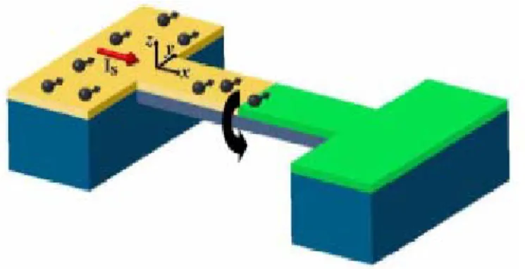
Fig. 1 : Schematic illustration of electromechanical spin current detector, containing a suspended semiconductor-mental (S-M) rectangular rod atop an insulating substrate (blue). A spin current is injected from the left semiconductor reservoir (yellow) and then diffuses toward the metallic film (green). While passing through the semiconductor film, the spin current induces torque shown by the black arrow.
thus a prime example of a single particle interferometer.[4] Various electronic interferometers with ballistic transport of the electrons have been investigated experimentally over the last decades, as e.g. Aharonov-Bohm (AB) rings[5] and double-slit interferometers.[6] Detailed investigations of dephasing in ballistic interferometers was carried out in Refs. [7,8]. Only very recently was the first electronic MZ-interferometer realized by Ji et al.[9] in a mesoscopic conductor in the quantum Hall regime. A high visibility of the conductance oscillations was observed, however the visibility was not perfect. This led the authors to investigate in detail various sources for dephasing. As a part of this investigation, also shot noise was measured. Still, some aspects of the experiment are not yet fully understood. Theoretically, Seelig and one of the authors [10] investigated the effect of dephasing due to Nyquist noise on the conductance in a MZ-interferometer. The effect of dephasing on the closely related four-terminal resistance in ballistic interferometers [11] was investigated as well. Dephasing in ballistic strongly interacting systems is discussed by Le Hur. [12,13] Following the experimental work of Ji et al.,[9]
Marquardt and Bruder investigated the effect of dephasing on the shot-noise in
MZ-interferometers, considering dephasing models based on both classical [14,15] as well as quantum fluctuating fields.[16] Very recently, Forster, Pilgram and one of the authors [17]
extended the dephasing model of Refs. [10,14] to the full statistical distribution of the transmitted charge.
The HBT-interferometer [18-20] was originally invented for stellar astronomy, to measure the angular diameter of stars. It is an intensity, or two-particle,[4] interferometer. The interference arises from the superposition of the amplitudes for two different two-particle processes.
Importantly, there is no single particle interference in the HBT-interferometer. Consequently, in contrast to the MZ-interferometer there is no interference in the light intensity, the interference instead appears in the intensity-intensity correlations. Moreover, the intensity-intensity
correlation also display the effect of quantum statistics. Photons originating from thermal sources tend to bunch, giving rise to positive intensity cross correlations. For the electronic analog of the HBT-interferometer, it was the corresponding anti-bunching of electrons that originally attracted interest. It was predicted [1] that the electrical current cross correlations in mesoscopic
conductors would be manifestly negative, i.e. display anti-bunching, as a consequence of the fermionic statistics of the electrons. Negative current cross correlations were subsequently observed in two independent experiments.[21,22] Recently, anti-bunching for field emitted electrons in vacuum was also demonstrated.[23] The two-particle interference in the
HBT-experiment has received much less attention. We emphasize that while the bunching of the photons was necessary for obtaining a finite, positive cross correlation signal, it was the
two-particle effect that was of main importance to HBT since the angular diameter of the star was determined from the two-particle interference pattern. In electrical conductors, two-particle effects in AB-interferometers were investigated theoretically in Refs. [24-26]. Only very recently two of the authors and Sukhorukov [27] proposed a direct electronic analog of the optical
HBT-interferometer which permits to demonstrate two-particle interference in an unambiguous way.
In this work we investigate and compare in detail the current and and zero-frequency noise in electronic MZ and HBT interferometers. We consider interferometers implemented in
single edge states and Quantum Point Contacts (QPC's) serve as controllable beam splitters. The effect of finite temperature, applied bias and asymmetry, i.e. unequal length of the interferometer arms, is investigated. The strength of the interference contribution is quantified via the visibility of the phase oscillations. The dependence of the visibility on the beam splitter transparencies as well as on the temperature, voltage and asymmetry is discussed in detail. Of interest is the comparison of visibility of the shot-noise correlation of the MZ-interferometer and the HBT-intensity interferometer. Shot noise correlations in the MZ-interferometer exhibit two contributions, one with the fundamental period of h/e and a second harmonic with period h/2e. The shot noise correlations in the HBT-interferometer, even though they are due to two particle processes, are periodic with period h/e. Thus the Aharonov-Bohm period can not be used to identify the two particle processes which give rise to the HBT effect. It is therefore interesting to ask whether the HBT two-particle processes have any other signature, for instance in the
temperature or voltage dependence of the visibility of the shot-noise correlation. We find that this is not the case. To the contrary, we find that the shot noise correlations in the HBT intensity interferometer behave qualitatively similar to the h/e shot noise correlation in the
MZ-interferometer. In contrast the h/2e contribution in the shot noise of the MZ-interferometer decreases more rapidly with increasing temperature, voltage or dephasing rate than the h/e oscillation in the MZ- or HBT-interferometer.
We investigate dephasing of the electrons propagating along the edge states by connecting one of the interferometer arms to a fictitious, dephasing voltage probe. In all cases, the current and noise of the MZ-interferometer as well as the noise in the HBT-interferometer, the effect of the voltage probe is equivalent to the effect of a slowly fluctuating phase.
[III] Transport characteristics of the dc spin current generation involving a quantum dot: Spintronics is important in both application and fundamental arenas [1,2,40]. The key issue of great interest is the generation of dc spin current (SC) without charge current. We proposed the SC generation via only one single ac-FG in a Rashba-type narrow channel [41]. A lot of methods have been proposed to generate and manipulate SC by utilizing optical excitation [42] , spin injection [43], and external magnetic field [44] in the QD system. More recently, another alternative method for generation and control of the SC is based on the Rashba-type spin-orbit interaction (SOI) in the narrow gap semiconductors [45].
The transport characteristics of metal-QD-metal structure have also been studied [46]. Utilizing the time-variation field to generate the SC has been studied in some mesoscopic systems in adiabatic [47] and non-adiabatic regimes [41,48]. Here, we consider a mesoscopic structure consisting of FG-QD-FG, where the FG is ac biased and QD is modeled by two delta potential in the quantum channel. The spin-dependent RIS mechanism makes the spin-dependent electron transit to its subband bottom such that the asymmetry spin-resolved transmission coefficients occur [41]. The spin-dependent RIS plays a crucial role while the incident energy is close to the resonance level or away nhΩ from resonance level in the QD. We find that the difference of spin-resolved transmission coefficients would be changed the sign depended on the incident energy. The spin-down transmission coefficient is larger than spin-up one TRL TRL
↓ > ↑ for incident
spin-down one TRL TRL
↑ > ↓ for the incident energy close to the satellite peaks with respect to the
resonance level.
Eventually, we obtain the dc SC without any charge current and opposite polarized direction for SC via varying the electron incident energy. Experimentally, we can tune the strength of two delta potentials to shift the energy of resonance main peak in order to change the switching point of the polarized direction of a SC. This tunable polarized direction of the SC is more valuable in the application of the spintronics device.
[IV] Effects of impurity on the dc spin current generation in a Rashba-type channel: We have proposed the dc SC generation via a ac-FG in Rashba-type quantum channel [41]. We are also interested in effects of the impurity for the transport of dc SC. The location and strength dependence of the impurity for the transport of dc SC has been studied. We find the effect of the impurity would be enhanced while the impurity is away from the channel-edge inside the ac-FG. The intersubband transition occurring near the subband bottom due to the translation invariance being broken. The impurity has smaller effect for the transport while the impurity is outside the ac-FG.
[V]
Dual-frequency modulation and sideband asymmetry characteristics in quantum transport through quantum dot:Quantum pumping effect has been an interesting topic [49-51]. In this work, we try to achieve quantum charge pumping in an alternative way by dual-frequency modulation instead of introducing a phase difference into the time-dependent potentials. Our goal is to find the optimal pumping modulation of the dual-frequency system, and also to get to understand the reasons electrons exhibit asymmetric sideband transmission characteristics.
[VI] The conductance of double quantum point contacts under de-phase process:
In experimental results, the phenomenon of double QPCs (quantum point contact) in series cannot be explained very well in classical theory. Because the conductance of one QPC will be quantized, however, in classical theoretical treatment, the total conductance of double QPCs in series still can observe the plateaus in curve. Here, we simply utilize an imaginary reservoir between the double QPCs to simulate the de-coherent effect related to the electron scattering process. This method can introduce a concept for the coherent length. We also can compare the de-well time and the lifetime via this method.
[VII ] The analytic analysis of Fano resonance transport through a mesoscopic two-lead ring:
The conventional Fano resonance is an effect due to the interference between resonant and non-resonant processes. It was first proposed in atomic physics [52], and the effect was then observed in a wide variety of spectroscopy such as the atomic photoionization [53], optical absorption [54], Raman scattering [55], and neutron scattering [56]. As recent progress in the technology of fabrication of electrical nano-devices has achieved devices with the size of the order of the inelastic length scales of the conduction electrons, where within the electronic
transport is ballistic, the Fano resonance is also seen in condensed matter systems. For instance, it is seen in the Scanning Tunneling Spectroscopy of a surface impurity atom [57,58], transport through a quantum dot (QD) [59-64] or carbon nanotube [65]. Moreover, it is proposed that the resonance can be used in the probe of phase coherence [66,67] and design of spin filters [68].
三、Results and discussion:
[I] Strain induced coupling of spin current to nanomechanical oscillations [70] (Appendix A).
[ II ] Visibility of current and shot noise in electrical Mach-Zehnder and Hanbury Brown Twiss interferometers (Appendix B).
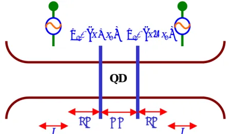
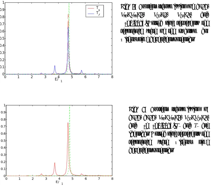
[III] Transport characteristics of the dc spin current generation involving a quantum dot: The system structure is shown in Fig. 1 and the QD is located between two ac-FGs. We use the scattering matrix method to deal with such problem. For simplicity, we suppose the symmetric structure such that the dc SC would be generated by ac-FG [1] without accompanying any charge current.
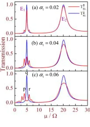
Figure 2 presents the spin-resolved transmission coefficients TRL
σ versus incident energy in the
unit of µ/Ω for various amplitudes
α
1 of the dynamic spin-orbit coupling constant. The notation TRLσ denotes that electron is incident from left-hand side terminal into the right-hand
side terminal with spin state
σ
. We observe the spin-resolved transmission coefficient TRL TRL↑ < ↓
for the incident energy around the resonance main peaks E1=4.93Ω and E2=20.13Ω. The other
features are TRL TRL
↑ > ↓ for satellite peaks which are away from each resonance main peak in
nhΩ. As increasing
α
1, the strength of inter-sideband transition become stronger such that thedifference of the spin-resolved transmission coefficients is enhanced due to the RIS through the resonance levels in the QD.
(
)
0 1V
δ
x
+
x
V0δ
(
x−x1)
L
L
FD
DD
FD
QD
Fig. 1: Schematic illustration of dc spin current generation involving a quantum dot on the Rashba-type quantum channel.
Figure 3 shows the SC corresponding to the figure 2 and the charge current is zero for our symmetric structure. The most interesting phenomena is that polarized direction of the SC have opposite sign while the incident energy of an electron passes the two resonance main peaks. It is because the difference of the spin-resolved transmission coefficients has the opposite-sign value for the resonance main peaks and satellite peaks, respectively.
We also find that the absolute value of the SC magnitude is larger in left-hand side of E1 (the first
resonance main peak) than that in the right-hand side of E1. It is because the larger difference of
Fig. 2: The spin-resolved transmission coefficient is plotted as a function of incident
energy /
µ
Ω for (a)α
1=0.02 , (b)1 0.04
α
= , and (c)α
1=0.06 . Otherparameters are spin-orbit coupling constant
0
α
=0.13, external frequency Ω =0.001(14GHz ), delta-type gate strength V0=0.4, the
ac-FG length L=35 (140nm), FD=20 (80nm), and DD=40 (160nm). There are several spin-resolved satellite peaks occurring away from the first resonance main peak. The two resonance main peaks are related to the energy
E1=4.93Ω and E1=20.13Ω, respectively.
Fig 3: The spin current related to the Fig. 2 is
plotted for
α
1=0.02(green), 0.04 (purple),and 0.06 (brown). The polarized direction of the SC is changed the sign while the incident energy of an electron passes the resonance
main peaks E1 and E2.
1 (a) 0.02
α
= 1 (b) 0.04α
= 1 (c) 0.06α
= E1 E2 p q r E1 E2spin-resolved transmission coefficients in the left-hand side of E1 due to the asymmetric satellite peaks. The absolute value of the SC magnitude is almost equal for the left-hand side and
right-hand side of E1 because of the unobvious asymmetric satellite-peak structures. The tunable
polarized direction of the SC is valuable to apply in the SC selector device based on time-modulated FG in the semiconductor device.
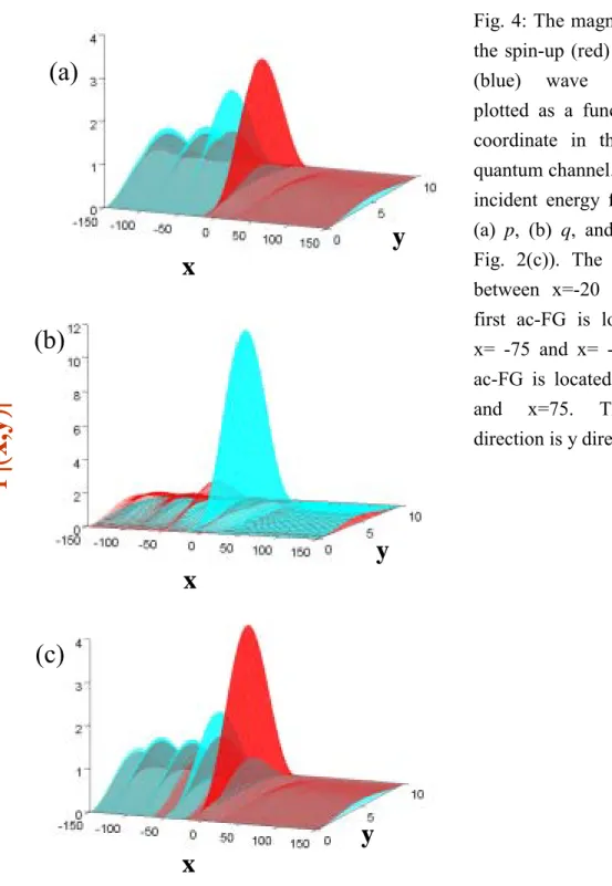
Ψ|(
x,y
)|
2
Fig. 4: The magnitude square of the spin-up (red) and spin-down (blue) wave functions are plotted as a function of spatial coordinate in the Rashba-type quantum channel. We choose the incident energy for three points (a) p, (b) q, and (c) r (see the Fig. 2(c)). The QD is located between x=-20 and x=20; the first ac-FG is located between x= -75 and x= -40; the second ac-FG is located between x=40 and x=75. The transverse direction is y direction.
We can observe that the magnitude square for spin-up wave function is smaller than spin-down wave function in Fig. 4 (b) in the transmission region (x>75) at the resonance main peak q corresponding to the relation TRL↑ <TRL↓ . For the satellite peaks p and r, the situation is reversed,
x
y
x
y
x
y
(a)
(b)
(c)
RL RL
T↑ >T↓ , in the transmission region. The spin-dependent wave functions are localized within the
QD for the resonance main peak and satellite peaks in standing-wave profile due to the resonance inelastic tunneling effect.
We use one-sideband approximation expressions of a single ac-FG to analyze the numerical results. The spin-resolved one-sideband transmission coefficients are expressed in the form of
All the spin-dependent difference comes from the spin-resolved wave vector kRLσ . Figure 5
presents the one-sideband approximation for the analytical and numerical results. Figure 5 (b) and
(c) reveal that the partial transmission coefficient T±1 is larger for the spin-up electron than the
spin-down one due to the RIS process. It shows that the one sideband-transition mechanism plays an important role for the difference of the spin-resolved transmission coefficients. While the incident energy is close to the resonance main peak, the spin-up electron is more easily to transit
to the satellite peaks via absorbing or emitting hΩ photon energy. For the energy around
satellite peaks, the transmission rate is barely low due to far from the resonance level in the QD.
It turns out the spin-up electron has lower transmission coefficient (TRL↑ <TRL↓ ) due to the larger
probability to transit to the satellite peaks for the spin-up electron. In the other hand, the incident energy of the electron coincides with the nearest satellite peaks away from the main peak such that the spin-up electron has larger probability to transit to the resonance main peak passing through the QD and we get the opposite result of TRL↑ >TRL↓ .
(
)
(
)
(
)
( )
(
)
(
)
(
)
( )
2 1 1 1 2 1 1 1 1 cos ( ) 2 4 2 ...(1). 1 cos ( ) 2 4 2 RL RL L T L T k k σ σ σ σµ
µ
α
α
µ
µ
µ µ
µ
µ
α
α
µ
µ
µ µ
µ
µ
− − − + Ω = − + Ω − + + Ω Ω − − − Ω = − − Ω − + Ω − Ω (a)
(b)
(c)
Fig. 5: The spin-resolved partial
transmission coefficients T and 0 T±1 are
plotted as a function of
µ
/Ω for a singleac-FG case. Other parameters are
0 0.13
α
= ,α
1=0.02, Ω =0.001, and theac FG length L=35. The dip structures are organized the quasi-bound state features
due to an electron emitting nhΩ photon
energy to transit to beneath of its subband bottom.
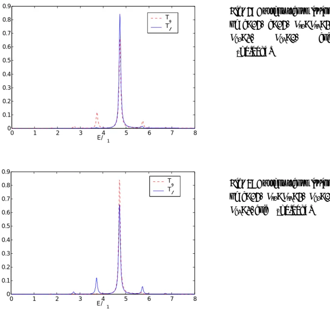
Next, we increase the strength V0 of the two delta potentials and the resonance levels are lift to
the higher energy. When the magnitude of V0 is enhanced, the band width of each resonance level
become more and more narrow in the QD. If we focus on the second resonance peak (purple
arrow), the satellite peaks (green arrows) would be resolved by increasing the strength of V0 in
Fig. 6 (a)-(c). The Fig. 6 (d) shows the resonance main peaks is shifted toward the higher energy
owe to the larger V0. The SC becomes smaller near the first main peak because the band width for
the main and satellite peaks is more narrow as increasing V0. We can tune the energy for the
switching points such that the spin-polarized direction of the SC would be changed its sign as its
incident energy crossing switching points via varying V0.
In summary, we have investigated the dc SC generation in sequent structure of ac-FG, QD, and ac-FG. The difference of the spin-resolved transmission coefficients is shown the opposite sign
while the incident energy occurring around the main peaks TRL TRL
↑ < ↓ and satellite peaks
RL RL
T↑ >T↓ , respectively. The switching point for the spin-polarized direction of SC can be tuned
by varying V0. We have proposed a possible setup to realize the device for SC selector based on
(a)V0=0.4
(b)V0=0.8
(c)V0=1.2
(d)
Fig. 6: The spin-resolved transmission coefficients are plotted as a function of
µ
/Ω withvarying the delta potential strength V0= (a) 0.4, (b) 0.8, and (c) 1.2. The SC is shown in
RIS mechanism involving a QD.
[IV]Effects of impurity on the dc spin current generation on a Rashba-type channel:
The finite-range impurity in the Rashba-type quantum channel is in the from
(
) (
) (
)
0 0 1 2
Vδ x−x θ y−y −θ y−y . The system configuration is show in Fig. 1 and the
transverse direction is finite-range potential with longitudinal delta profile potential.
The dc SC can be generated via a single ac-FG without any charge current [41]. The resonance inelastic scattering (RIS) play a important role to make the spin-resolved transmission coefficient asymmetry. The Fig. 2 presents the spin-resolved transmission coefficients and SC versus
incident energy µn/Ω for no impurity case.
Fig. 1: The system configuration is shown and the finite-range impurity (red) can be located
inside or outside of the ac-FG. The blue block is ac-FG, V0 is the impurity strength, l is the
FG length and W is the channel width.
(
) (
) (
)
0 0 1 2V
δ
x
−
x
θ
y
−
y
−
θ
y
−
y
x
y
y=y
1y=y
2 W0
1
2
3
0
5
10
15
20
0.0
0.2
0.4
0.6
Transm
iss
ion
T
RLT
RLSp
in Cu
rr
en
t (
nA)
µ
/
Ω
Fig. 2: The spin-resolved transmission coefficients and spin current versus
/
n
µ Ω is plotted for no impurity case.
Other parameters are: static SOI
coupling constant α0 =0.13 , the
dynamic SOI amplitude α1 =0.05 ,
oscillating frequency Ω =0.002
(28GHz), channel width W=50, and the ac-FG length l=20. The spin-resolved dip structures is due to the RIS mechanism.
While the impurity is located in the channel edge inside of the ac-FG, the effect of the impurity is small for the transport of dc SC. Figure 3 presents the transmission and dc SC versus incident
energy /µn Ω as increasing the impurity strength V0. All of their SC are almost the same and it
shows the weak effect of impurity for the transport of dc SC.
While the impurity is away from the channel edge, the effect of the impurity is more obvious in Fig. 4. We also observe the structure of the intersubband transition near the arising of the second and third subband bottom due to breaking the translation invariance in transverse direction. As increasing the impurity strengths, the spin-resolved dip structures become more broaden due to the impurity scattering.
While the impurity is away from the channel edge outside of the ac-FG, the effect of impurity is smaller than inside of the ac-FG. The spin-resolved transmission coefficients and SC is shown in Fig. 5. The spin-resolved dip structures are not obvious broaden in this case providing the effect of the impurity is weaker outside of the ac-FG than inside of the ac-FG.
In summary, effects of impurity on transport of dc SC depend on the locations and strength of the impurity. The impurity affects the dc SC is not very strong such that the dc SC generation via a single FG is valuable in application of spintronics devices even in diluted-impurity case.
Fig.3: The spin-resolved transmission coefficients and SC is plotted as function of µn/Ω for
varying the impurity strength V0. The impurity is located in the channel edge for x0=0, y1=0,
and y2=4. Other parameters are the same as Fig.2.
0
1
2
3
0
1
2
3
0
5
10
15
20
0
1
2
3
T
ran
sm
issio
n
µn/
ΩT
RLT
RL0
5
10
15
20
0.0
0.1
0.2
0.3
0.4
0.5
0.6
0.7
Spin Cur
re
nt
(nA)
µn/
Ω V0=0.1 V0=0.2 V0=0.3 (a) V0=0.1 (b) V0=0.2 (c) V0=0.3Fig.4: The spin-resolved transmission coefficients and SC is plotted as function of µn/Ω
for varying the impurity strength V0. The impurity is located in the channel edge for x0=0,
y1=8, and y2=12. Other parameters are the same as Fig.2.
0
1
2
3
0
1
2
3
0
5
10
15
20
0
1
2
3
Tr
an
sm
is
sio
n
µn/
ΩT
RLT
RL0
5
10
15
20
0.0
0.2
0.4
0.6
0.8
Sp
in
C
urre
nt
(n
A)
µn/
ΩV
0=0.1
V
0=0.2
V
0=0.3
(a) V0=0.1 (b) V0=0.2 (c) V0=0.3Fig.5: The spin-resolved transmission coefficients and SC is plotted as function of µn/Ω
for varying the impurity strength V0. The impurity is located in the channel edge for x0=-15,
y1=8, and y2=12. Other parameters are the same as Fig.2.
0
1
2
3
0
1
2
3
0
5
10
15
20
0
1
2
3
T
ransm
is
si
on
µn/
Ω TRL TRL0
5
10
15
20
0.0
0.2
0.4
0.6
0.8
Spin
Cu
rr
en
t (n
A)
µn/
Ω V0=0.1 V0=0.2 V0=0.3 (a) V0=0.1 (b) V0=0.2 (c) V0=0.30 0.05 0.1 0.15 0.2 0 0.1 0.2 0.3 0.4 0.5 0.6 0.7 0.8 0.9 1 E δV=0 δV=-2 δV=2
[VI] Dual-frequency modulation and sideband asymmetry characteristics in quantum transport through quantum dot:
a. Shifting of resonance levels
In this subsection, we discuss the shifting of the resonance levels in an open quantum dot confined by Vs1 on the left and Vs2 on the right.
0 0.05 0.1 0.15 0.2 0 0.1 0.2 0.3 0.4 0.5 0.6 0.7 0.8 0.9 1 E V=1 V=2 V=3
Fig. 1: Total current transmission coefficient of a quantum dot with a=15, and Vs1=Vs2=V.
As shown in Fig. 1, we acquire sharper resonance states with stronger confinements to a quantum dot, but broader and lower ones with weaker static confinements. The transmission
coefficient of each case achieves 1. In Fig. 2, when we add an additional part δV to one of the
static barriers making the quantum dot asymmetric, the resonance levels also shift to higher
energies or lower energies when δV is, respectively, positive or negative. Another interesting
feature in Fig. 2 is that the transmission coefficient does not achieve 1 when the quantum dot is asymmetric.
Fig. 2: Total current transmission coefficient of a quantum dot with a=15, Vs1=3, Vs2=V+δV.
We then apply time-dependent potential(s) to the confinement of a quantum dot. The magnitude of the confining barrier will change periodically. Therefore, resonance levels will also shift with time, but the overall effect (after time averaging) of the shift is towards lower-energy end. This can be referred back to Fig. 3.1.2. The degree of shifting towards lower energy is greater than that of shifting towards higher energy, making the overall effect shift to the left. In Fig. 4, we applied two oscillating barriers to the quantum dot. The shift of resonance state is therefore further enhanced.
b. Sideband Characteristics
In this subsection, we discuss sideband characteristics under several different time-dependent modulations on the confinement of the open quantum dot.
Sideband Features of Single Oscillating Potential:
Only one time-dependent potential is applied to the confinements of the quantum dot. Either Vd1cosΩ1t is applied on the left, or Vd2cosΩ2t is applied on the right of the quantum dot.
0 1 2 3 4 5 6 7 8 0 0.1 0.2 0.3 0.4 0.5 0.6 0.7 0.8 0.9 1 E/Ω1 T → T ←
Fig. 3: Current transmission of a=15,
Vs1=Vs2=3, Vd1=0, Vd2=2, and
Ω2=0.0084. Dotted line represents the
resonance state of the quantum dot without time dependent potential.
0 1 2 3 4 5 6 7 8 0 0.1 0.2 0.3 0.4 0.5 0.6 0.7 0.8 0.9 1 E/Ω1
Fig. 4: Current transmission of a=15, a=15, Vs1=Vs2=3, Vd1=Vd2=2, and Ω1=Ω2=0.0084. T→ and T← are
identical. Dotted line represents the
resonance state without time
(Ι) Ω2=Ω1:
Fig. 5 and Fig. 6 are complementary to each other due to the same oscillating frequency,
exhibiting the same sideband features. In Fig. 5, because only Vd1cosΩ1t is applied to the
quantum dot (applied on the left of the quantum dot), sideband characteristics for electrons incident from the right is not as notable as those of electrons incident from the left.
(ΙΙ) Ω2=nΩ1:
Within this case we set Ω2=2Ω1, and, again, either Vd1cosΩ1t is applied on the left, or Vd2cosΩ2t is applied on the right of the quantum dot.
In Fig. 7, 8, and Fig. 9, we can see that sideband structures for T→ are more significant,
whereas sideband structures are more significant for T← in Fig. 8, and Fig. 9.
When only Vd1cosΩ1t is applied, electrons incident from the right seem to be “screened” by
Vs2 before encountering the oscillating barrier. Hence, it’s easier for electrons incident from the
left to make transition by resonance levels when Vd1cosΩ1t is applied, therefore making the
side-peak features more significant. The condition totally reverses when Vd2cosΩ2t is applied on
0 1 2 3 4 5 6 7 8 0 0.1 0.2 0.3 0.4 0.5 0.6 0.7 0.8 0.9 E/Ω1 T→ T←
Fig. 5: Current transmission
of a=15, a=15, Vs1=Vs2=3, Vd1=2, Vd2=0, and Ω1=0.0084. 0 1 2 3 4 5 6 7 8 0 0.1 0.2 0.3 0.4 0.5 0.6 0.7 0.8 0.9 E/Ω1 T→ T ←
Fig. 6: Current transmission of a=15, Vs1=Vs2=3, Vd1=0, Vd2=2, and Ω2=0.0084.
the right of the dot.
c. Double Oscillating Potentials (Ι) Ω2=Ω1:
In Fig. 10, only T→ is shown because T→ and T← are exactly the same under such symmetric
condition. The special feature is that side-peak structures are more notable at the left of the
0 1 2 3 4 5 6 7 8 0 0.1 0.2 0.3 0.4 0.5 0.6 0.7 0.8 0.9 E/Ω1 T → T← 0 1 2 3 4 5 6 7 8 0 0.1 0.2 0.3 0.4 0.5 0.6 0.7 0.8 0.9 E/Ω1 T → T ← 0 1 2 3 4 5 6 7 8 0 0.1 0.2 0.3 0.4 0.5 0.6 0.7 0.8 0.9 E/Ω1 T→ T←
Fig. 7: Current transmission of a=15, Vs1=Vs2=3, Vd1=2, Vd2=0, and
Ω1=0.0084.
Fig. 8: Current transmission of a=15,
Vs1=Vs2=3, Vd1=0, Vd2=2, and
Ω2=2Ω1=0.0168.
Fig. 9: Current transmission of a=15,
Vs1=Vs2=3, Vd1=0, Vd2=2, and
resonance state implying electrons are more possible to absorb n-Ω1 energy from the system.
d. Sideband Features When Resonance States Approach Subband Bottom
From Fig. 3.2.9 and Fig. 3.2.10 we find that the relative strength of the two sidepeaks beside the resonance state will reverse when approaching subband bottom.
0 1 2 3 4 5 6 7 8 0 0.1 0.2 0.3 0.4 0.5 0.6 0.7 0.8 E/Ω1
Fig. 10: Current transmission of a=15, Vs1=Vs2=3, Vd1=Vd2=2, and Ω2=Ω1=0.0084. 0 1 2 3 4 5 6 7 8 0 0.1 0.2 0.3 0.4 0.5 0.6 0.7 0.8 E/Ω1 a=21 a=22
Fig. 11: Current transmission
of Vs1=Vs2=3, Vd1=Vd2=2, Ω1=Ω2=0.0084 under a=21, and a=22. 0 1 2 3 4 5 6 7 8 0 0.1 0.2 0.3 0.4 0.5 0.6 0.7 0.8 E/Ω 1 a=23
a=24 Fig. 12: Current transmission
of Vs1=Vs2=3, Vd1=Vd2=2,
Ω1=Ω2=0.0084 under a=23,
[VI] The conductance of double quantum point contacts under de-phase process:
The double QPCs with de-coherent scattering process [69] have been studied and the structure is shown in the Fig. 1.
1 1.5 2 2.5 3 3.5 4 4.5 5 0.4 0.5 0.6 0.7 0.8 0.9 1 w 2 G total ε=0 ε=0.2 ε=0.4 ε=0.6 ε=0.8 ε=1 w 1=1 w3=20 E=1.5 G1=0.9992
The de-coherent strength parameter is εand E is the incident energy. It represents how the de-coherent strength influents the total conductance.ε=0 occurs when double QPCs in series when coherent length is infinite. If de-coherent strength is raising up, the total conductance approaches the classical theoretical results and the de-coherent process increases the resistance so the total conductance is lowering down.
w1 w2
w3
1 3 Fig. 1: Our model is a double
constriction with a cavity region. The narrow constriction can be regarded as a quantum point contact [70]. The dimensionless unit of length is 1/kf.
Fig. 2: In classical picture, a QPC can be regarded as a resistance related to its width. This figure shows calculated total conductance as a function of the width of QPC2 for various de-coherent strength. The width of QPC1 is fixed.
1 1.5 2 2.5 3 3.5 4 4.5 5 0 1 2 3 4 5 6 w 1=1 w3=20 E=1.5 ε=1 w 2 G 1 1.5 2 2.5 3 3.5 4 4.5 5 0.6 0.8 1 1.2 1.4 1.6 1.8 2 2.2 2.4 2.6 G total ε=0 ε=0.1 ε=0.3 ε=0.5 ε=0.7 ε=1 w 1=3 w3=20 E=1.5 G 1=3.0143 w 2 1.35 1.4 1.45 1.5 1.55 1.6 0.6 0.8 1 1.2 1.4 1.6 1.8 2 G w1=3 w3=20 w2=2 ε=0 E 1.35 1.4 1.45 1.5 1.55 1.6 1.8 2 2.2 2.4 2.6 2.8 3 w1=3 w3=20 w2=4 ε=0 E G
Fig. 5: The theoretical conductance for double QPC in series is plotted as a function of incident energy.
We can obtain the dip structure when we check the relation between total conductance and incident energy in Fig. 4. At the same incident energy of Fig. 3, the Fig. 5 (a) is the normal case and we can find dip structure in Fig. 5 (b). It supports our above theoretical assumption.
Fig. 3: It is shown the double QPC are fully de-coherent. So the total conductance is the conductance for two QPC in series. Green line is the conductance of QPC2 and be quantized conductance as an individual QPC [71].
Fig. 4: For the specific case, the total
conductance is increased when
de-coherent strength is turned on. The reason is the resonance occurs in such specific case.
[VII ] The analytic analysis of Fano resonance transport through a mesoscopic two-lead ring:
Unequal armlengths:
We investigate the case of different armlengths in the ring but clean transport channel. This is
described by M1=M2=1 and the transmission amplitude A3 is reduced to
(
)
(
)
(
)
(
(
)
)
(
(
)
)
1 2 3 1 2 1 2 1 2 sin sin 11 exp cos cos
4 i kL kL A ik L L k L L k L L + = − − + − + − − ……….(1)
The observation of the detuned zeroes in the numerator and denominator directly implies that the above numerical results can be casted into the usual Fano resonance expression, and the relation between the resonant dip's width and detuning from perfectly constructive 2PI be investigated more closely. To be self-contained, first we give a very brief review of the Fano resonance discussed in Fano's original paper. In a tunneling process, if there simultaneously involves a non-resonant tunneling, which is almost energy independent and can be simply described by a
complex-valued tunneling amplitude t , and a resonant tunneling at incident energy 0 ε=0 which
can be approximately described by a complex-valued tunneling amplitude tr =za/(ε+ia),
where z is a complex-valued number describing the relative strength of the non-resonant and
resonant tunneling, and a is a real-valued number characterising the width of the resonant
tunneling. The total tunneling amplitude would be ttot = + = +t0 tr (ε qa) /(ε+ia), and the total
tunneling robability T= ttot 2 would be
M
2M
1x
0x
3x
1x
2x
1x
2 x0=0 x1=L1 x2=L2 x1=x2=x3=0Fig. 1: The generic system we consider has two
leads. The boxes on the ring labeled M1,2
represent the scatters. A coordinate system xiis
defined for the line segment labeled by i (i=1, 2 and 3). While the arrows denote the increasing direction of the coordinates, the right Y-junction is defined at x1 =x2 =x3=0, and the left Y-junction is at x0=0, x1=L1, and x2=L2.
2 2 0 2 2 T= t qa a ε ε + + …………..(2)
where q z/t≡ 0+i, is the Fano parameter. We will briefly describe the behavior of the above
tunneling probability. In the case of a 0≠ , when q 0≠ , T gives a dip/peak when the
numerator/denominator in Eq.2 is close to zero. When q=0, T has only a dip at ε =0. The
case of Im q=0 is discussed comprehensively in Fano's original paper. In the case of a →0,
the numerator and denominator in Eq.2 can become exact zeroes but, they are all first order
zeroes at =0ε and hence they cancel each other and gives a finite transmission amplitude. This
is actually just the case of commensurate armlength ratio L2/L we have discussed. Since we 1
have analytically found that all the dips can only appear at k=km, where km(L1+L2) 2= mπ
and m is an integer defines k , we expand the tunneling amplitude m A near a dip by letting 3
1 2
(k km)(L L )
δ = − + . Since we also know that the dips appear when km(L1−L2) 2≠ nπ, where
n is an integer, we define a detuning from a perfectly constructive 2PI δ by
1 2
( ) 2
m
k L −L = nπ δ+ , where ∆ is from −
π
to +π (note that given an m$m$, n$n$ isdetermined). Then we expand A at the vicinity of a dip when both the dimensionless 3 δ and
∆ are small. We have expanded Eq.1 for the case of max( )
δ
: ∆ and ∆ =π
. We expandthe numerator to the third order and the denominator to the second order, and we obtain an approximate transmission amplitude
3 3 2 1 2 1 2 2 3 3 1 2 1 2 2 2 1 2 1 2 2 1 2 1 2 1 1 1 ( 1) 1 8 4 6 ( ) . 1 1 1 5 8 4 8 m n L L L L A L L L L L L L L i L L L L
δ
δ
δ
δ
δ
δ
+ − + − − ∆ − ∆ − × + + − − + ∆ + ∆ − − + + ; …………..(3)The fractional part can be viewed as a q=0 Fano resonance with a δ -dependent width, and
the part other than the fractional part can be viewed as an envelope function. It is seen that within
this range of δ the line shape is not in the conventional Fano form. But if we further restrict
ourselves to the range of
δ
is an order of magnitude smaller than ∆, i.e., max( )δ
: ∆2, theexpression in Eq. 3 can be further simplified to
2 3 ( 1) (1 8 ) 2 , 8 m n A i
δ
δ
+ ∆ − − ∆ + ; ……….(4)which is exactly in the form of the conventional q=0 Fano resonance, which has only a dip.
Note that the parameter
δ
is a dimensionless wavevector but not energy. When the detuning ∆approaches zero, the width of the dip (: ∆2) approaches zero and the dip becomes infinitely
sharp and vanishes. There are a few noteworthy points here. If one adopts the conventional understanding of the Fano resonance lines with the usual notions of quasibound states and their lifetimes, the ``lifetimes'' of the ``quasibound states'' our case might seem can be drastically tuned by a slight tuning of the armlength ratio! Moreover, the two arms of the ring are all the same
besides their lengths, and the SWR at k L( 1+L2) 2= m
π
also occurs in the entire ring, thereforehere.
On the other hand, we also have investigated the transmission amplitude A for the case of 3
1 2
L =L =L, in the complex wave number k% plane. This is a common way to investigate the
quasibound states in the tunneling paths, the states in the ring in our case. In this special case of
1 2
L =L =L, we can readily find poles at kL%=n
π
−iLn3, where n is an integer. Though theRe k% does correspond to a standing wave in an isolated ring with circumference 2L , the Im k%
is large and comparable to the spacing in the Re k%. This indicates that these ``quasibound'' states
are vaguely defined and this is in congruent with the fact that the ring is open. It is also inappropriate to view any of these states signified by the poles as a quasibound state in Fano's original formalism, which always gives a peak-dip pair profile at near the quasibound state energy. In spite of this, the transmission dips can be created and sharp. As we will see in the later subsections, these standing wave states are also related to the formation of the peak-dip pairs in thetransmission spectrum when impurity potential is included.
It is thus seen that the conventional Fano resonance scheme with straightforward notions like non-resonant and resonant tunneling paths, lifetime of the quasibound states, might be hard to provide a consistent understanding basis of the above results of equal armlengths and slightly unequal armlengths. This reveals the logic that though when there are resonant and non-resonant paths in a tunneling process there will be a Fano resonance line, the reversed statement, when there is a Fano lineshape then there are resonant and non-resonant tunneling paths in the tunneling process, may {\it not} be always true. In other words,though the mathematical form of the resulting tunneling probability can be unanimously in the Fano form as in Eq. 2, the physical contents could be quite different.
Single impurity
This subsection considers the case of a point impurity is embedded into the ring. The
impurity is described by a Dirac-δ function potential and this model should be applicable for
local potentials with extensions small compared with the wavelengths of the itinerant electrons and armlengths of the ring. The impurity is embedded into arm 1 by adding the potential
1 ( 1 1)
V
δ
x −X , where V is the strength of the impurity and 1 X is the location of the impurity in 1coordinate x on arm 1, and the corresponding transfer matrix is 1
1 1 2 1 1 2 2 1 2 1 1 2 2 1 M 1 i kX i kX imV imV e k k imV imV e k k − − − = + h h h h ………(5)
Henceforth we will use the dimensionless parameter 2
1 1 1/(2 )
impurity strength. It is noted that the transfer matrix has the symmetry 11 22 *
1 1
M =(M ) and
12 21 *
1 1
M =(M ) . Arm 2 is clean and henceM2 =1.
Figure 2 shows how the asymmetric Fano-type resonance arises as the strength of the
impurity on arm 1 grows. We have chosen L1 =L2 and X1/L1=0.3 in Fig. 2. Such a peak-dip
line shape resonance is in contrast with the mere dip resonance in the without impurity case, but both of them are seen to develop from zero widths. However small the width of the Fano resonance, it is seen that the peaks always reach one and the dips always reach zero. Mathematically the dips are also due to the lift of zeroes in the denominator D . It is noted that the dips are not necessarily at the eigenenergies of an isolated ring with a point
impurity. When the impurity strength becomes considerable, the dips depend very much on the location of the impurity since both the impurity and Y-junctions have a substantial effect on the standing waves in the ring. At the strong impurity limit, the zero transmission dips are wide and
located at kX and1 k L( 1−X1) integer= ×π , and that agrees with the result of a 1D wire with
stubs. The arm is essentially cutoff when the impurity is strong, and our case is equivalent to a
1D wire with two stubs of lengths X and 1 L1−X1 attached. There will be zero transmission
when the length of any one stub is such that an integral number of half-wavelengths can just be fitted in.
Fig. 2: The transmission probability T is shown versus the dimensionless
wave number kL1/(2π) for L1=L2 and
a point impurity at X1/L1=0.3 with
strength v1=0.2, 0.8, and 10 (cutoff
limit) [From (a) to (c)]. Each of the panels has a height of 1. The Fano resonance lines are seen to collapse at
the limit v1=0 by shrinking their
widths. The square roots of the magnitude of the numerator C and denominator D of the transmission
amplitude, C (red) and
D (blue), are also plotted [in (d)]
for v1=0.8 to illustrate how the Fano