Nano-composite Recording Layers Applied to Write-once
High-density Optical Data Storage
Hung-Chuan Mai and Tsung-Eong Hsieh*
Department of Materials Science and Engineering, National Chiao-Tung University, 1001
Ta-Hsueh Rd., Hsinchu 30010, Taiwan, ROC
ABSTRACT
This work demonstrates the feasibility of composite thin film containing nano-scale recording particles to high-density optical data storage. For an HD-DVD format “nano”-optical disk containing such a nano-composite layer, modulation higher than 0.5 was achieved when 11T and 4T signals were respectively written into the disk by using a blue-laser dynamic tester. Transmission electron microscopy (TEM) characterization attributed the recording mechanism to the grain coalescence/coarsening and crystallinity change of nano-recording particles which, in turn, results in sufficient reflectivity difference for signal readout. The utilization of nano-composite recording layers may drastically simplify the optical disk structure and thus is a promising alternative for next-generation write-once data recording.
Keywords: Nano-composites recording layer, HD-DVD, optical data storage.
1. INTRODUCTION
Presently digital versatile disks (DVDs) with storage capacities ≥ 4.7 GB are popular media for information management and multimedia data storage. The recently proposed high-density digital DVD (HD-DVD) and Blu-ray (BD) disks are recognized as the recording media for next-generation optical data storage. The recording materials for write-once HD-DVD and BD disks can be either organic dyes [1-2] or inorganic metallic alloys [3], e.g., phase-change GeSbTe-based alloys [4], single-layer AlSi alloy [5-6], bi-layer metals such as Cu/Si [7], Cu/a-Si [8], GeCu/Si [9], Zn/a-Ge [10],metallic nitrides [11], etc. Conventional DVD disks usually comprised of complicated multilayer structures including lower/upper dielectric layers, recording layer, space layer and reflection layer. In order to simplify the disk structure, composite layer constituted by nano-scale quaternary alloy recording particles embedded in silica matrix was prepared by sputtering process and was subsequently implanted in an HD-DVD disk for write-once recording applications. The signal properties, microstructure and signal readout mechanisms of disk samples were investigated and the feasibility of nano-composite layer applied to optical recording was evaluated.
2. EXPERIMENTAL PROCEDURES
The optical disk samples were prepared by using a self-designed six-target sputtering system at a background pressure better than 10−6 torr. Two types of HD-DVD format optical disk samples were prepared: type I disk contains sequent layers of PC substrate, 100-nm thick silver (Ag) reflection layer and nano-composite recording layer (Fig. 1(a)) and type II disk contains PC substrate and a sole nano-composite recording layer (Fig. 1(b)). The part of type I disk was subjected to initialization before
signal writing in order to evaluate its necessity. Figure 1(c) depicts the layer structure of conventional HD-DVD disk for the purpose of comparison. After the sputtering deposition, another PC substrate was glued on to form the HD-DVD disk samples [12]. The nano-composite recording layer was prepared by target-attachment method that an adequate amount of AgInSbTe quaternary alloy pellets are placed on a quartz target during sputtering. The optical disks constituted by various thicknesses of nano-composite recording layers and reflection layers were prepared. Their optimum writing power (Pw) and
modulation were evaluated by using a dynamic tester (ODU-1000, PULSTEC) equipped with a 405-nm blue laser diode and a numerical aperture (NA) = 0.65. Microstructure and composition changes of nano-composite recording layer subjected to laser writing were examined by using a Jeol FX-II 2010 TEM in conjunction with energy dispersive spectroscopy (EDS, Link ISIS 300). The plan-view TEM (PTEM) samples were prepared in accordance with the method reported by Chen et al. [13].
3. RESULTS AND DISCUSSION
Figure 2 presents the TEM microstructure of the as-deposited nano-composite layer. The nano-scale quaternary alloy particles about 5 nm in sizes randomly embedded in silicamatrix could be seen. The diffuse ring pattern revealed by the selected area electron diffraction (SAED, see attached pattern on upper left-handed corner of Fig. 2) indicates the recording particles embedded in the as-deposited layer are of amorphous structure. Figures 3 displays the reflectivity change of nano-composite recording layers as a function of temperatures measured at various heating rates. It can be seen that the nano-composite recording layers exhibit an abrupt reflectivity change at about 200°C regardless of the heating rates.
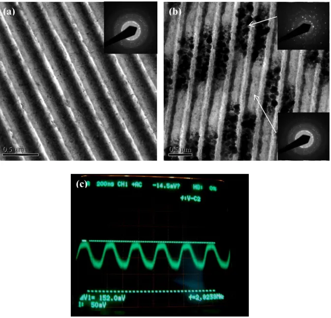
Figure 4(a) shows the PTEM image of type I disk subjected to initialization. The attached SAED pattern evidences the completion of recrystallization despite of particle coarsening in the nano-composite layer. Initialization is required for conventional disks in order to achieve sufficient reflectivity difference [14]. In this study, initialization was carried out in type I disk samples to evaluate its necessity for satisfactory signal properties. Figure 4(b) shows the PTEM image of 11T signal marks written in the type I optical disks. The recording marks about 1.2 µm in length located at the groove regimes of optical disk can be clearly seen and aggregation of coarse particles about 100 to 200 nm in sizes comprises of each of the marks. Apparently, the nano-scale recording particles coalesced and coarsened under the irradiation of laser beam. Comparisons of SAED patterns taken from mark and non-mark areas indicate that the coarse particles in mark regime are arranged in a less random manner. The distinct microstructure change (i.e., the differences of grain sizes and crystallinity in mark and non-mark areas) provided sufficient reflectivity difference for signal readout and hence high modulation value. The EDS analysis revealed a relatively high Ag element signal in mark regimes. This indicated that laser heating also causes the diffusion of Ag in reflection layer into the nano-composite recording layer. Hence the composition change in mark regime should also contribute the reflectively change for signal readout. Figure 4(c) presents the waveform of 11T signals written in type I disk sample at the linear speed of
Proc. of SPIE Vol. 6620 66202F-2
6.61 m/sec. Subsequent analysis revealed the corresponding modulation is higher than 0.5, surpassing the requirements of HD-DVD specification [12].
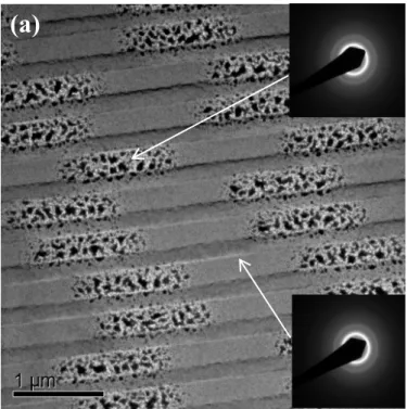
TEM image of 11T signal marks written in type II optical disk at optimized Pw = 7 mW is given in Fig. 5(a)
and the waveforms corresponding to 11T and 4T signals read directly from oscilloscope are presented in Figs. 5(b) and 5(c), respectively. The lower writing power for type II “nano”-optical disk is attributed to the elimination of metallic reflection layer in optical disks which reduce the consumption of laser heating. Figure 5(a) clearly reveals the coarse particles constitute the mark areas. The broad ring pattern shown in attached SAED pattern taken from the mark area in type II disk sample reveals that the mark regime remains amorphous after laser writing. Hence the nano-scale recording particles experienced only coalescence and coarsening during signal writing. The modulation values deduced from Figs. 5(b) and 5(c) were found to be 0.8 and 0.6 for 11T and 4T signals, respectively, and hence such a coarse-grained microstructure still provides sufficient reflectivity difference for signal readout in type II disk samples. This result further indicates that initialization process might be eliminated in the disk samples containing nano-composite layer prior signal recording.
4. CONCLUSIONS
Signal property and microstructure characterizations on two types of HD-DVD format optical disks demonstrate the feasibility of nano-composite recording layer to optical data storage. The mechanism of signal recording was mainly attributed to the coalescence and coarsening of nano-scale particles in the recording layer when laser beam was irradiated on. Promising applications to next-generation high-speed optical data storage is expected as it possesses advantages such as fast phase transition rate, disk structure simplification and sputtering-compatible fabrication process.
ACKNOWLEDGMENTS
This work was supported by the National Science Council of the Republic of China under contract NSC93-2216-E-009-008. Dynamic test supplied by Prodisc Technology Inc., Taiwan,
Figure 1. Cross-sectional structures of (a) type I, (b) type II “nano”-optical disk samples and (c) conventional HD-DVD disk.
Figure 2. TEM micrographs of as-deposited nano-composite recording layer. The inserted SAED pattern at upper left-handed corner indicated the recording layer is amorphous.
PC substrate Reflection layer Recording layer PC substrate Dielectric layer Dielectric layer Nano-composite recording layer PC substrate Reflection layer PC substrate Nano-composite recording layer PC substrate PC substrate (a) (b) (c)
Nano-scale recording particles
Proc. of SPIE Vol. 6620 66202F-4
Figure 3. Reflectivity change of nano-composite recording layers as a function of temperatures at various heating rates.
0
100
200
300
400
500
R
efl
ec
ti
vit
y
(a.u
.)
Temperature
120
°C/min
100
°C/min
60
°C/min
40
°C/min
Figure 4. PTEM micrographs of type I disk sample (a) subjected to initialization and (b) the 11T signal marks written in an optimized disk sample. (c) is the waveforms for 11T signals written in type I disk sample The inserted SAED patterns in (a) and (b) indicate the cyrsyallinity change of nano-composite recording layer in disk samples.
(a)
(b)
(c)
Proc. of SPIE Vol. 6620 66202F-6
A 300n5 GUI
=
fl? HOt as
41YC2 H-V H-V V V V V V iVI. 0.458 9fSI.SIfl
ItI0o.V
Figure 5. (a) TEM micrograph of 11T signal marks written in the type II optical disk at optimized Pw = 7 mW
and signal waveforms corresponding to (b) 11T and (c) 4T read directly from oscilloscope. The SAED patterns attached in (a) are taken from mark (upper right-handed corner) and non-mark (lower right-handed corner) areas, respectively.
(a)
References
1. E. Hamada, et al., Jpn. J. Appl. Phys., 39, 785 (2000). 2. H. Nishiwaki, et al., Jpn. J. Appl. Phys., 45, 1452 (2006). 3. N. Sasa, et al., Jpn. J. Appl. Phys., 43, 4972 (2004). 4. N. Ishii, et al., Jpn. J. Appl. Phys., 41, 1691 (2002). 5. B. M. Chen and R. L. Yeh, Proc. SPIE., 5380, 141 (2004). 6. B. M. Chen, et al., Jpn. J. Appl. Phys., 43, 5018 (2004). 7. A. E. T. Kuiper, et al., Appl. Phys. Lett., 86, 221921, (2005). 8. Y. C. Her and C. L. Wu, Jpn. J. Appl. Phys., 43, 1013 (2004). 9. S. H. Ma, et al., APDSC, 140 ( 2006 ).
10. C. P. Liu, et al., APDSC, 172 ( 2006 ).
11. Y. Hosoda, et al., Jpn. J. Appl. Phys. 43, 4997 (2004).
12. DVD Specifications for High Density Recordable Disc (HD DVD-R) for Blue Laser Optical System, Version 0.9, The DVD forum, July, 2004.
13. H. W. Chen, T. E. Hsieh, J. R. Liu and H. P. D. Shieh., Jpn. J. Appl. Phys., 38, 1691 (1999). 14. P. K. Bhatnagar, G. Mongia, P. C. Mathur, Opt. Eng., 42, 3274 (2003).
Proc. of SPIE Vol. 6620 66202F-8