Nanofabrication and the structure-property analyses of phase-change
alloy-ended CNTs
W.H. Wang, K.M. Chao, I.J. Teng, C.T. Kuo *
Department of Materials Science and Engineering, National Chiao Tung University, Hsinchu, Taiwan Available online 13 October 2005
Abstract
In order to cap the tip cavities of the open-ended carbon nanotubes (CNTs) with the phase-change alloy for potential applications as the nano-resolution storage media, the Co-assisted CNTs were first synthesized by electron cyclotron resonance chemical vapor deposition (ECR-CVD) with H2and CH4as the gas sources. Then, the as-grown CNTs were post-treated in H-plasma atmosphere to remove the carbon
layers covered on catalysts, and subsequently immersed in HNO3solution to remove the catalysts from the tips. The open-ended CNTs with a
bowl-like-shape tips were followed by coating with a phase-change alloy layer of GeSbTeSn via sputtering process, and then heat treated in vacuum for 30 min to trim the alloy off from the sidewalls of CNTs to obtain the alloy-ended CNTs. The structures and properties in each processing step were characterized by scanning electron microscopy (SEM), transmission electron microscopy (TEM), Raman spectroscopy and Auger electron spectroscopy (AES).
The experimental results show that the well-oriented phase-change alloy-ended CNTs over a large area are fabricated successfully. Furthermore, the Auger analyses show the compositions of the phase-change alloys may be changed from Te-rich to Ge-rich after being capped on the tips of CNTs.
D 2005 Elsevier B.V. All rights reserved.
Keywords: Phase-change; Carbon nanotubes (CNTs); Electron cyclotron resonance (ECR); Chemical vapor deposition (CVD)
1. Introduction
CNTs have some unique physical and chemical properties such as ultrahigh mechanical strength[1], excellent electronic
[2] and thermal conductivity[3], etc. Therefore, the CNTs attract much interest in academic and technology commun-ities in the past few years. Some special applications, i.e. single electron transistor [4], may come true because the diameter of CNTs can achieve the scale of few nanometers by process control. More than the size effect, the encapsulated metal CNTs also bring dramatic application, i.e. ultra-high-density magnetic storage. Bao et al. have fabricated an array of nickel-filled CNTs to prove the possibility[5].
The phase-change alloys have been commercially used for optical storage applications in rewritable digital versatile disks (DVD). Basic concepts of the mechanisms
for the phase-change applications are the different optical properties between amorphous and crystalline state such as reflectivity. Except for the optical property change, the remarkable electrical property change of phase-change materials between amorphous and crystalline state also brings amazing application. Recently, phase-change alloy materials are widely studied for the application of solid state memory such as Phase Change Random Access Memory (PC-RAM) via the electrical resistivity change with few orders between amorphous and crystalline state [6].
In this study, CNTs were expected to make a link with phase-change alloy to be a nano-resolution storage device. In order to realize the goal of ultra-high-density storage, the technology of nanofabrication of phase-change alloy-ended carbon nanotubes was developed and their structure proper-ties at each processing step were studied. We provide a potential technology to realize ultra-high-density storage in this work.
0257-8972/$ - see front matterD 2005 Elsevier B.V. All rights reserved. doi:10.1016/j.surfcoat.2005.07.011
* Corresponding author. Tel.: +886 3 5731949; fax: +886 3 5724727. E-mail address: ctkuo@mail.nctu.edu.tw (C.T. Kuo).
2. Experimental
First, a layer of 100-nm-thick cobalt film was deposited on the Si wafer via sputtering process to act as the catalyst for CNTs deposition. Then, the Co film on the Si wafer was pretreated by H-plasma etching to become well-distributed nanoparticles and subsequently were deposited under various CH4/H2 atmospheres (CH4/H2: 10/10, 20/10 and 10/20 sccm/sccm) to form carbon nanostructures by ECR-CVD system. The pretreatment conditions were: microwave power, 800 W; magnetic field, 875 G; H2flow rate, 15 sccm; substrate temperature, ¨ 630 -C; substrate bias, 150 V; chamber pressure, 10 3Torr; and treating time of 15 min. The CNTs deposition conditions were: pressure, 10 3Torr; substrate temperature, 655-C; 150 V bias; 15 min. deposition time.
After the deposition of carbon nanostructures, the as-grown close-ended CNTs were post-treated by 1-min H-plasma etching to remove the carbon layer covered on catalyst, and then immersed in nitric acid for 3 min to remove the catalysts to form open-ended CNTs [7]. The other parameters of H-plasma etching of post-treatment were: temperature ¨ 150-C; bias, 200 V, pressure ¨ 10 3Torr; magnetic field, 875 G; microwave power, 575 W and H2flow rate, 10 sccm.
The open-ended CNTs were subsequently coated with a GeSbTeSn phase-change alloy (Ge, 28 at.%; Sb, 11 at.%; Te, 55 at.%; Sn, 6 at.%) layer of 200 nm in thickness by sputtering process and then were followed by heat treatment under 420-C for 30 min. The purpose of the heat treatment is to assist the phase-change materials infiltrate into the
hollow of CNTs and clean the residual materials on the wall of CNTs. The morphologies and characteristics of CNTs in each process are characterized by FESEM (Hitachi S-4000), TEM (JEOL 2000FX), Raman spectroscopy (Jobin Yvon LabRam HR) and Scanning auger microscopy (SAM, VG Microlab 310F).
3. Results and discussion
3.1. Effects of CH4/H2ratio on CNTs growth and bonding structure
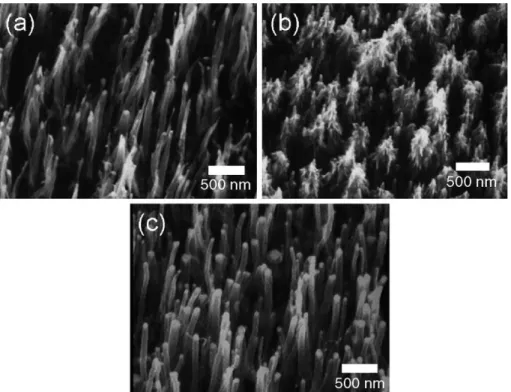
First, the well-aligned CNTs were fabricated over a large area on a silicon wafer by ECR-CVD. To control the morphology of the as-grown CNTs effectively, the CH4/H2 ratio was varied to examine its effect in synthesizing process. The SEM images of Co-assisted grown CNTs under various CH4/H2ratio of 10/10, 20/10 and 10/20 sccm/ sccm are shown inFigs. 1(a), (b) and (c), respectively. The SEM result represents that CH4/H2ratio can determine the morphologies of carbon nanostructures. An overabounding carbon concentration in the gas phase is a more favorable condition for continuously depositing on the sides of catalysts to form rattan-like CNTs as shown in Fig. 1(b). The formation of rattan-like CNTs can be suppressed by decreasing CH4 or increasing H2 flow rate. The tube diameters of well-aligned close-ended CNTs are ¨ 80 nm and tube number densities are ¨ 3.89 G tube/in.2, as shown inFig. 1(c), this is in agreement with the previous report that the diameter of CNTs is closely associated with the size of
the catalyst particles [8]. Furthermore, it indicates that the diameter and distribution of the well-oriented CNTs can be controllable via process parameters. It implies that recording density can be increased remarkably by reducing the tube size and increasing the tube density when each tube is considered as a recording mark.
To examine the bonding structure of grown CNTs, the Raman spectra are shown in Fig. 2. The ID/IG ratio is decreased as the CH4/H2 ratio decreases, it implies that amorphous carbon can be preferentially etched off and the CNTs are left under higher H2 concentration [9]. In summary, the well-aligned close-ended CNTs over a large area with lower ID/IG ratio can be fabricated under lower CH4/H2ratio by Co-assisted ECR-CVD method.
3.2. H-plasma and chemical etching post-treatment for the open-ended CNTs
In order to fabricate the open-ended CNTs, post-treat-ment was applied on as-grown close-ended CNTs. The SEM and TEM images of tubule-like CNTs etched by 1-min H-plasma and followed by 3-min chemical etching (0.25 M HNO3) are shown inFigs. 3 and 4, respectively. Under the
present conditions, to open caps of tubule-like CNTs, the two-step post-treatment contains 1-min H-plasma etching and 3-min 0.25 M HNO3etching is capable to maintain the structure integrity of CNTs and to remove the catalysts completely to form open-ended structure at the tip[7]. This highly oriented open-ended CNTs can provide a promising template for phase-change alloy materials infiltration in next process step.
3.3. Structure and composition variations by high temper-ature tip trimming
Phase-change alloy are infiltrated into the CNTs via sputtering and heat-trimming processes. The SEM image of open-ended CNTs coated with 200 nm phase-change alloy is shown in Fig. 5, it shows the tube diameter increases due to the phase-change alloy covering on the stems of CNTs. The SEM image of phase-change
alloy-Fig. 3. SEM micrograph of the as-grown CNTs after post-treatments (H-plasma etching and chemical etching) showing the open-ended structure.
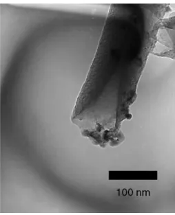
Fig. 4. The corresponding TEM micrograph ofFig. 3.
Fig. 5. SEM micrograph of open-ended CNTs covered with phase-change alloy of 200 nm in thickness.
coated CNTs after heat treatment at 420-C for 30 min is shown inFig. 6. It shows that the alloy-coated open-ended CNTs can be heat-treated to trim off the alloys from their sidewalls in vacuum at 420 -C for 30 min to become alloy-ended CNTs.Fig. 7is the corresponding TEM image of Fig. 6, it indicates that phase-change materials covered at the tip were successfully infiltrated into the hollow of CNTs and the tube diameter of CNTs is reduced to its original size (¨ 80 nm).
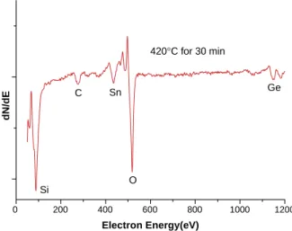
It is interesting to note that the melting point of GeSbTeSn alloy is ¨ 640 -C in bulk state but it was evaporated away at 420-C due to the size effect. To clarify the properties of phase-change alloy-ended CNTs, the auger analysis result is shown in Fig. 8. It indicates the composition of phase-change alloy after being capped on the tips of CNTs may be changed from Te-rich to Ge-rich due to the faster evaporation rates of Sb and Te (Sb and Te have lower melting point and heat of vaporization than Ge). On the other hand, the composition and physical properties of phase-change alloy would be changed owing to the heat-treatment process and size effect. If we wish to obtain the
expected composition of phase-change alloy in nano-scale as bulk state, it is necessary to modify the composition or deposition process parameter.
4. Conclusions
The well-aligned phase-change alloy-ended CNTs over a large area are successfully fabricated in this work. The processes include catalyst-assisted CNTs growth, H-plasma post-treatment, chemical etching, phase-change layer sput-tering and heat trimming. The remarkable features of this method are: (i) simple and well-productive process to fabricate well-aligned metal-filled CNTs with large area, and (ii) the diameter, length and structure of metal-filled CNTs are controllable via experimental parameter. Fur-thermore, the Auger analyses show that the sputtering process must be modified to obtain the required compo-sition of phase-change alloy after being capped on the tips of CNTs. An array of highly oriented phase-change alloy-ended CNTs fabricated in this work may offer highly opportunity for the application of nano-resolution storage device.
Acknowledgments
This work was supported partly by the National Science Council of Taiwan, under Contract No. NSC93-2216-E-009-004, NSC93-2216-E-009-009, and NSC93-2120-M-009-003.
References
[1] M. Treacy, T.W. Ebbesen, J.M. Gbson, Nature 381 (1996) 678. [2] R. Saito, M. Fujita, G. Dresselhaus, M.S. Dresselhaus, Appl. Phys. Lett.
60 (1992) 2204.
[3] P. Kim, L. Shi, A. Majumdar, P.L. McEuen, Phys. Rev. Lett. 87 (2001) 21550-1.
Fig. 7. The corresponding TEM micrograph ofFig. 6.
0 200 400 600 800 1000 1200 420°C for 30 min Si C Sn O Ge dN/dE Electron Energy(eV)
Fig. 8. Auger spectrum of phase-change alloy-ended CNTs. Fig. 6. SEM micrograph of open-ended CNTs covered with phase-change
[4] Y.T. Tan, T. Kamiya, Z.A.K. Durrani, H. Ahmed, J. Appl. Phys. 94 (2003) 633.
[5] J. Bao, Q. Zhou, J. Hong, Z. Xu, Appl. Phys. Lett. 81 (2002) 4592. [6] Research report from Ovonics, http://www.ovonic.com/PDFs/Elec_
Memory_Research_Report/OUM.pdf(1999).
[7] K.M. Chao, Master thesis, (2004), Mat. Res. Lab. MSE, NCTU. [8] L.C. Qin, D. Zhou, A.R. Krauss, D.M. Gruen, Appl. Phys. Lett. 72
(1998) 3437.