A PARALLEL COUPLED-LINE FILTER USING VLSI
BACKEND INTERCONNECT WITH HIGH
RESISTIVITY SUBSTRATE
C. C. Chen,1 H. L. Kao, K. C. Chiang, and Albert Chin
Institute of Electronics Engineers, National Chiao Tung University 1001 Ta-Hsueh Road, Hsinchu, Taiwan 30050, R.O.C
Received 3 October 2005
Abstract
This paper reports our progress in developing parallel coupled-line filters based on Si-based VLSI backend interconnects for millimeter-wave applications. The resonant frequency of this coupled-line filter increases with increasing spacing-gap and with increasing IDM thickness. By using high resistivity substrate, the parallel coupled-line band-pass filter is extremely effective in reducing substrate loss, and also provides very low insertion loss, even at the millimeter-wave regime. In addition, the parallel coupled-line filter suitable for advanced system-on-a-chips at the millimeter wave application achieves high performance characteristics, which show low insertion loss, wide band, and compatibility with standard VLSI process.
Keywords: parallel coupled-line filter, VLSI, high resistivity substrate,
millimeter-wave.
1. Introduction
The strong demand on advanced wireless communication services for advanced system-on-a-chips has attracted a great deal of attention. This is due
to their significant benefits such as overall chip size reduction, lower fabrication cost, as well as enhanced system performance. Meanwhile, significant progress in advanced VLSI technology [1] has made it possible to realize system-on-a-chip at millimeter-wave frequencies [2]. The concept of integrating parallel coupled-line filters with CMOS integrated circuit on silicon (Si) substrate is appealing because shorter coupling-line has shown on backend local or globe interconnects with CMOS scaling down [3]. This requirement becomes even more urgent as the operation frequency of Si communication integrated circuits (ICs) increases. However, the performance of microwave filters integrated on Si [4] suffers from the high frequency losses and crosstalk of the low resistivity Si substrate [5]. This is the fundamental limitation of Si-based RF circuits [6]. To improve the high-frequency performance of band-pass filter, in this paper, we present our recent progress in implementing the VLSI backend interconnects [7], a novel interconnect concept for millimeter-wave silicon MMIC’s using high resistivity substrate technology, which can reduce losses from Si substrate [8]. The superior performance of the parallel coupled-line filter [9] in broadband and insertion loss denotes its applicability to advanced millimeter-wave wireless communication systems.
2. Design and fabrication
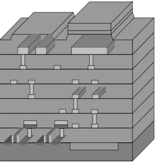
To imitate the interconnects, such as those shown schematically in Fig. 1, two long coupled lines were fabricated with lengths of 1 mm long and with different line-spacing of 10, 5, and 2.5 Pm. Different inter-metal dielectric (IMD) thickness of 0.7 or 6 Pm were used to simulate the local or global interconnects using metal-1 (M1) or metal-6 (M6) layers of the 1-Poly-6-Metal (1P6M) structures shown in Fig. 1.
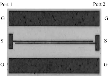
Fig. 2 shows the die photo of fabricated 1 mm coupled lines with 10 Pm spacing width, where additional co-planar waveguide (CPW) structure and 150 Pm spacing GSG probing pads were used to study the parallel coupled-line filter. The CPW coupled lines were fabricated by 2 Pm thick Al metal on
PECVD deposited IMD SiO2 above the Si substrate. The S21 and S11 are the signal transmission from port 1 to port 2 and return loss of port 1, respectively. This approach was necessary due to non-ideal open and shortin the RF regime. For comparison, we also investigated coupled lines on high-resistivity Si (HRS) substrates, which had a resistivity of 1.5u104
ȍ-cm. The fabricated coupled lines were characterized by S-parameters measurements using an HP8510C network analyzer with standard RF calibration up to 50 GHz. The EM simulation results using IE3D (Zeland Software) were also demonstrated for comparison.
Fig. 1. The standard VLSI process on a Si-based technology showing
Fig. 2. The die photo of a fabricated 1 mm length parallel coupled-line filter
with 10 Pm gap-spacing width.
3. Experimetal results and discussion
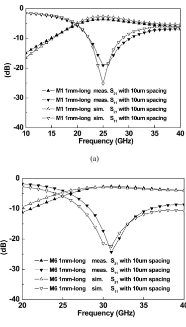
Fig. 3(a) shows the simulated and measured results for a 1 mm long interconnect parallel coupled-line filter with 10 Pm spacing-gap on 0.7 Pm SiO2-isolated low-resistivity Si (LRS) substrates (M1). At the resonant frequency of 25 GHz, the poor RF characteristics of measured band-pass filter, such as the insertion loss of 3.6 dB, are unacceptable for filter use. However, this structure of parallel coupled-line filter based on VLSI backend interconnects has the advantage of integrating microwave and millimeter wave devices into the ICs. The measured result is in good agreement with the simulated result, which implies that the IE-3D simulator is reliable for verifying.
For comparison, the simulated and measured results for a 1 mm long interconnect parallel coupled-line filter with 10 Pm spacing-gap on 6 Pm SiO2-isolated low-resistivity Si substrates (M6) are also plotted in Fig. 3(b). From the measured and simulated results, we can find that the resonant
Port 1 Port 2 G S G G S G
frequency increases as the IMD thickness increases. In addition, it can be seen that the simulated and measured insertion losses are almost the same at the resonant frequency, which are 2.73 dB and 2.94 dB respectively. The slight reduction of insertion loss and the shifted resonant frequency in this coupled-line filter are apparently due to the increasing IMD thickness as compared with Fig. 3(a). However, the insertion loss and the bandwidth are still inadequate for advanced wireless communication application at high frequency range.
10 15 20 25 30 35 40 -40 -30 -20 -10 0
M1 1mm-long meas. S21 with 10um spacing M1 1mm-long meas. S11 with 10um spacing M1 1mm-long sim. S21 with 10um spacing M1 1mm-long sim. S11 with 10um spacing
(d B) Frequency (GHz) (a) 20 25 30 35 40 -40 -30 -20 -10 0
M6 1mm-long meas. S21 with 10um spacing M6 1mm-long meas. S
11 with 10um spacing
M6 1mm-long sim. S21 with 10um spacing M6 1mm-long sim. S11 with 10um spacing
(dB
)
Frequency (GHz)
(b)
Fig. 3. The measured and simulated S21 and S11 responses for 1 mm long, 10 Pm-spaced parallel lines filter on (a) 0.7 Pm SiO2-isolated Si LRS (b) 6ҏ Pm SiO2-isolated Si LRS.
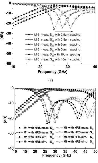
From the view of advanced VLSI backend process, we also made a study of a 1 mm long interconnect parallel coupled-line filter with different spacing-gap of 2.5 Pm, 5 Pm, and 10 Pm on 6 Pm SiO2-isolated low-resistivity Si substrates (M6) in Fig. 4(a). It is seen that the resonant frequency increases from 25, 28, to 31 GHz with the increasing of the spacing-gap in 2.5 Pm, 5 Pm, and 10 Pm. Meanwhile, the insertion losses of measured results are 3.1, 2.81 and 2.63 dB for each resonant frequency, respectively. From this result, it is more effective to enhance the resonant frequency of the parallel coupled line filters by increasing the spacing-gap between the two coupled-lines than increasing the IMD thickness. Taking the optimized geometry of spacing-gap between two coupled-lines, the expected resonant frequency of this parallel coupled line filters can be extracted. That will offer a good choice to design the filters.
By using high resistivity silicon substrate (HRS), the measured S21 and S11 responses of 1 mm long interconnect parallel coupled-line filter with 10 Pm spacing-gap shown in Fig. 4(b). The simulation for ideal designed filters is included for comparison. From the figure, the S11 response of the measured parallel coupled-line filter on 0.7 Pm SiO2-isolated HRS shows good performance in enhancing its stop-band characteristics, which has two transmission zeros at 26 GHz and 41 GHz with an attenuation level of 23.4 dB and 19.7 dB, and the S21 response is as small as 1.1 dB at the central frequency of 33.5 GHz. The in-band insertion loss has a minimum of 0.3 dB at 26 GHz and increases smoothly with frequency. Besides, the simulated and measured S21 and S11 responses of 1 mm long interconnect parallel coupled-line filter with 10 Pm spacing-gap on 6 Pm SiO2-isolated HRS also are plotted in Fig. 4(b). The central frequency of this measured parallel coupled-line filter is shifted to 38.5 GHz with the measured S21 of 1.4 dB, and the two rejection bands of that are centered at frequencies of 30 and 46 GHz, respectively. The flat insertion loss in the pass-band, with a minimum of 0.4 dB, is suitable for the band-pass filters using at the millimeter-wave range.
The great improvement in the insertion loss and bandwidth as compared with those shown in Fig. 3 is due to the high resistivity Si substrate that reduces the loss paths. The central frequency of this band-pass filter increases with the IMD thickness and the good characteristics of this band-pass filter, such as low insertion loss, broad bandwidth, integratable with VLSI technology, and extending its bandwidth at millimeter wave regime are all demonstrated by this parallel coupled-line filter basing on the HRS substrate.
10 20 30 40 -60 -50 -40 -30 -20 -10 0 (dB) Frequency (GHz)
M 6 meas. S21 with 2.5um spacing M 6 meas. S11 with 2.5um spacing M 6 meas. S21 with 5um spacing M 6 meas. S11 with 5um spacing M 6 meas. S21 with 10um spacing M 6 meas. S11 with 10um spacing
(a) 10 15 20 25 30 35 40 45 50 -40 -30 -20 -10 0 M6 with HRS meas. S21 M6 with HRS meas. S11 M6 with HRS sim. S21 M6 with HRS sim. S11 M1 with HRS meas. S21 M1 with HRS meas. S11 M1 with HRS sim. S21 M1 with HRS sim. S11 (dB) Frequency (GHz) (b)
Fig. 4. (a) Comparison of S21 and S11 responses for 1 mm long parallel lines filter using with different spacing-gap of 2.5, 5, and 10 Pm on 6 ҏPm SiO2-isolated Si LRS. (b) The measured and simulated S21 and S11 responses of 1 mm long, 10 Pm-spaced parallel lines filter on 0.7 Pm and 6 ҏPm SiO2-isolated Si HRS.
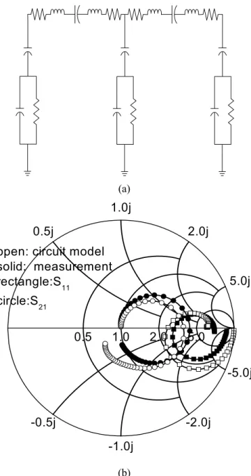
Fig. 5(a) shows the equivalent circuit model of the interconnect parallel coupled-line filter. The equivalent circuit of the substrate RC network includes the Cox, which is the capacitance contributed by the IMD SiO2, and the Rsub and the Csub, which are the shunt resistance and capacitance modelling the effect of lossy silicon substrate. In the equivalent circuit of the two coupled line, L1 and R1 are the series inductance and parasitic resistance of the interconnect line body, L2 and R2 are the series inductance and parasitic resistance of the nearby interconnect line body, and the Ccouple is the coupling capacitance between the two parallel coupled-lines. In order to verify this equivalent circuit, Fig. 5(b) shows the S-parameter result for a 1 mm long interconnect parallel coupled-line filter with 10 Pm spacing-gap on 6 Pm SiO2-isolated LRS substrates. The consistency between the measured and modeling results from S-parameter proves that the equivalent circuit is suitable for modelling the parallel coupled line filter. Besides, the modelling results reveal that, using an HRS substrate, leakage losses from the substrate RC network can be significantly reduced, therefore improving high-frequency performances.
(a)
0.5
1.0
2.0
5.0
-0.5j
0.5j
-1.0j
1.0j
-2.0j
2.0j
-5.0j
5.0j
open: circuit model
solid: measurement
rectangle:S
11circle:S
21 (b)Fig. 5. (a) The equivalent circuit of two parallel coupled interconnect lines with
4. Conclusion
High performance millimeter-wave band-pass filters based on standard VLSI backend process are successfully demonstrated. By using the high resistivity Si substrate, the parallel coupled-line filters have good characteristics such as low insertion loss, broadband, and compact size. This novelty of using VLSI backend interconnect with high resistivity substrate provides an attractive solution for low-cost high-performance wireless application up to millimeter-wave frequency range.
Acknowledgment
The authors thank Director and Prof. Tsu-Jae King at EECS of the UC-Berkeley for his help in this work. This work was partially supported by the joint of NRC-Canada and NSC (94-2215-E-009-062)-Taiwan grant
References
[1] K. C. Sarawat and F. Mohammadi, “Effect of interconnection scaling on time delay of VLSI circuits,” IEEE Trans. Electron Devices, vol. 29, pp. 645-650, 1982.
[2] J. Kim, Y. Qian, G. Feng, P. Ma, M. F. Chang, and T. Itoh, “Millimeter-wave silicon MMIC interconnect and coupler using multilayer polymide technology,” IEEE Trans. Microwave Theory Tech., vol. 48, pp. 1482-1487, 2000.
[3] H. Iwai, “Future semiconductor manufacturing: challenges and opportunities,” IEDM Tech. Dig., 2004, pp. 11-16.
[4] K. T. Chan, A. Chin, Y. B. Chen, Y.-D. Lin, D. T. S. Duh, and W. J. Lin “Integrated antennas on Si, proton-implanted Si and Si-on-quartz,” IEDM Tech. Dig., 2001, pp. 903-906.
[5] Y. H. Wu, A. Chin, K. H. Shih, C. C. Wu, S. C. Pai, C. C. Chi, and C. P. Liao, “RF loss and cross talk on extremely high resistivity (10K-1Mȍ-cm) Si fabricated by ion implantation,” IEEE MTT-S Int. Microwave Symp.
Dig., vol. 1, 2000, pp. 221-224.
[6] J. Papapolymerou and G. E. Ponchak, “Microwave filters on a low resistivity Si substrate with a polyimide interface layer for wireless circuits,” IEEE Radio Frequency Integrated Circuits (RFIC) Symp. Dig., 2001, pp. 125-128.
[7] K. Kim, H. Yoon and K. K. O, “On-chip wireless interconnection with integrated antennas,” IEDM Tech. Dig., 2000, pp. 485-488.
[8] T. Ohguro, K. Kojima, H. S. Momose, S. Nitta, T. Fukuda, T. Enda, and Y. Toyoshima, “Improvement of high resistivity substrate for future mixed analog-digital application,” VLSI Tech. Dig., 2002, pp. 158-159.
[9] S. B. Cohn, “Parallel-Coupled Transmission-Line-Resonator Filters,” IEEE Trans. Microwave Theory Tech., vol. 6, pp. 223-231, 1958.