A modi®ed multi-chemical spray cleaning process for post shallow trench
isolation chemical mechanical polishing cleaning application
Y.L. Wang
a,*, T.C. Wang
b, J. Wu
a, W.T. Tseng
a, C.F. Lin
caTaiwan Semiconductor Co., Ltd, Hsinchu 300, Taiwan
bInstitute of Material Science and Engineering, National Chiao-Tung University, Hsinchu, Taiwan cInstitute of Material Science and Engineering, National Cheng-Kuan University, Tainan, Taiwan
Abstract
Chemical mechanical planarization (CMP) has become widely accepted for the formation of device interconnect structures. Shallow trench isolation technology (STI) utilizes CMP and has been applied to deep-sub-micron processes. Poly Si, CVD Si or SiO2can be grown or deposited in the trench and planarized by a CMP process. However, the typical wafer surface is contaminated with slurry particles and metallic impurities after the CMP process. The silica particles may damage the VLSI patterns and the metallic impurities can induce many crystal defects in Si wafers during the following furnace processing. Therefore, the post CMP clean is a very important step for the STI process. However, the wafer for poly-Si surface is hydrophobic, SiO2surface is hydrophilic and Si ®lm is very easy to charge up. Thus, the defect can be dif®cult to remove by a conventional cleaning technique. In this study, we propose the use of a modi®ed multi-chemicals spray cleaning process for post STI CMP cleaning. We used a modi®ed and heated ammonia/peroxide mix (APM) clean with an ammonia pre-soak and an HF step to etch a thin layer for the removal of trapped metallic ions which can be followed by a hydrochloric/peroxide mix (HPM) clean process to assist in the removal of metallic ions. q 1998 Elsevier Science S.A. All rights reserved.
Keywords: Chemical mechanical polishing; Shallow trench isolation; Post-CMP cleaning; Multi-chemicals spray cleaning
1. Introduction
As device geometrics have continued to shrink and circuit complexity has continued to grow, the device isolation has become a major factor limiting the circuit density. The tradi-tional local oxidation of silicon (LOCOS) has a limitation for sub-half micron generation due to the lateral encroach-ment of ®eld oxide upon the device active areas, ®eld oxide thinning in sub-micron regions of exposed silicon, non-planarity, and stress-induced silicon defects [1]. In order to increase the device package density for high performance VLSI/ULSI technology, the shallow trench isolation (STI) process becomes attractive. STI improves the isolation between devices where compared to conventional LOCOS-type isolation techniques [2-5]. Although, the CMP process is well recognized as a powerful method for global planarization, several issues associated with CMP including dishing, oxide remaining above nitride and post-CMP cleaning have to be resolved before STI can be fully replace LOCOS.
During the CMP process, the wafer surface is contami-nated with silica particles and metallic impurities. These
defects can introduce many crystal defects in Si wafers during furnace processing, since the planarization of STI is carried out at the front-end-of-line. However, the removal of the defects is dif®cult because the poly-Si or Si substrate surface is hydrophobic and SiO2surface is hydrophilic and
the surface of silicon nitride is easily charged up [5]. In this paper, we introduce a modi®ed multi-chemical spray clean-ing process for post STI CMP cleanclean-ing process to assist in the removal of the defects and metallic impurities.
2. Experiment
In this paper, all of the data presented was obtained from testing 200-mm wafers. The STI ®ll was deposited by the sub-atmospheric chemical vapor deposition (SACVD, 450 Torr) technique which was a TEOS base system. Figs. 1 and 2 show the STI process and trench scheme. First of all, the LPCVD nitride deposited 150,200 nm and after pattern de®ne and trench etching, the STI was formed. The depth of the trench is 350 nm and trench density is 36%. The SACVD was deposited 600 nm on pattern wafers and was subsequently polished 200 nm.
The polishing process was performed on Applied Mirra polisher multi-head, multi-platen system. Table 1 shows the
Thin Solid Films 332 (1998) 385±390
0040-6090/98/$ - see front matter q 1998 Elsevier Science S.A. All rights reserved. PII S0040-6090(98)01207-3
* Corresponding author. Tel.: 1886 3 5781688; fax: 1886 3 5790298; e-mail: ylwang@tsmc.com.tw.
detail parameters of STI CMP in the Applied Mirra polisher. The polishing pads were IC1000/Suba-IV perforated pads made by Rodel. The KOH-based colloidal fumed silica slurry (SS-12) from Cabot was used for the oxide CMP. The modi®ed multi-chemicals spray cleaner used in this study had a standard FSI MERCURY spray cleaner and a SCREEN AS-2000 Post-CMP processor with PVA brush. The APM (ammonia/peroxide mix) and HPM (hydrochlo-ric/peroxide mix) was heated before being delivered to the chamber in the FSI system. Most of the cleaning recipe was modi®ed and followed the procedure formulated by Kern and Puotieu at RCA, which is often referred to as the RCA method [6]. Table 2 lists the clean recipes used in this study. The performance after the cleaning process was exam-ined for both particle defects and metallic contaminates on wafers. The metallic contamination was measured by Rigaku-3630 TXRF and defects on the wafer were
measured by a KLA digital comparison system. Surface roughness was examined by atomic force microscopy (AFM). The thickness of oxide loss on the pattern wafer during cleaning was measured by a Nano SPEC 8000 system.
3. Results
All of the polished wafers were cleaned in the spray processor using different chemicals. The combined effects
Fig. 1. The STI process scheme.
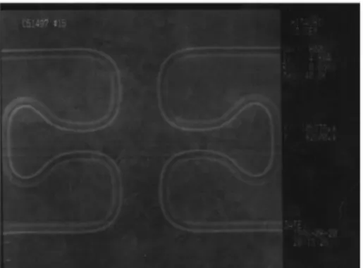
Fig. 2. The SEM picture of STI.
Table 1
The parameters of the STI recipe in Mirra
Step 1 Step 2 Step 3 Step 4
Plate rev./min/acc 0/30 10/5 30/5 80/5
Head rev./min acc 0/30 10/5 30/5 80/5
Head sweep No sweep No sweep Sinusoidal sweep Sinusoidal sweep
Polish I-tube Vented Vented Vented p4.0 psi
Ret ring Vacuum p2.0 psi p5.0 psi p5.5 psi
Check membrane Vacuum Vacuum p2.0 psi p4.5 psi
Delivery 1 Slurry200 ml Slurry200 ml Slurry200 ml Slurry200 ml
Delivery 2 No No No No
of APM, HPM and dilute HF scrubber were evaluated on the surface of wafers. Fig. 3 shows the trend chart of particles removed for different cleaning chemical ratios of NH4OH in
the APM. From the results, the particle removal ef®ciency is very sensitive to the NH4OH content in the APM. In order to
improve particle removal results, the combined effect of APM, dilute HF scrubbing and HPM was also evaluated. In order to eliminate the possibility of poor surface rough-ness after a HF dip, different dilute HF treatments were also examined. Table 3 lists the results for different combined cleaning recipes.
From the results of Table 3, the combined cleaning recipes for APM, dilute HF scrubber and HPM exhibit an excellent defect level. The metal ion contamination after
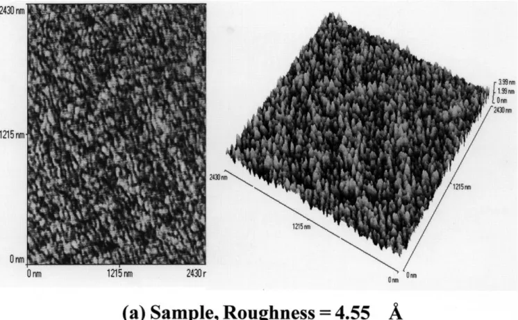
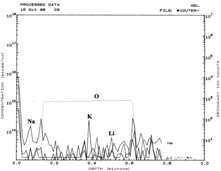
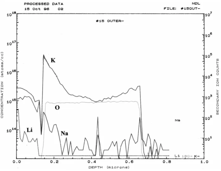
CMP polishing can be removed by using a dilute HF scrub. For dilute HF scrubber 15 s is enough for the defect and metallic contamination removal, the HF scrubber 30-s treatment will result in more oxide loss and worse surface roughness. The sequence of `HF scrubber prior to APM' shows a worse defect and metal level than `APM prior to dilute HF scrubber'. Figs. 4 and 5 show the comparison picture between `APM1HF scrubber 15 s1HPM clean' and `HF scrubber only' on AFM. Figs. 6 and 7 show the SIMS analysis for `APM1HF scrubber 15 s1HPM clean' and `HF scrubber only'. In order to eliminate the surface ¯uctuation for SIMS analysis, we have deposited 0.1 mm low temperature amorphous silicon ®lm on the oxide surface with Applied P-5000 chambers before the SIMS measurements.
4. Discussion
For STI post-CMP clean results from the above informa-tion, there is a concept of zeta potential that could be used to explain the results. The enhanced cleaning ability of NH4OH and H2O2solutions is believed to be explained by
a strong relationship that exits between the pH value and zeta potentials of these solutions and other materials present in the cleaning environment. Malik and Zhang [7] studied the relationship between zeta potential and silica, alumina and tungsten. It is believed that when the zeta potential of a silica particle and the oxide surface are the same sign, either positive or negative, defects will be easier removed from the wafer surface due to the electrical repulsive forces. The pH
Y.L. Wang et al. / Thin Solid Films 332 (1998) 385±390 387 Table 2
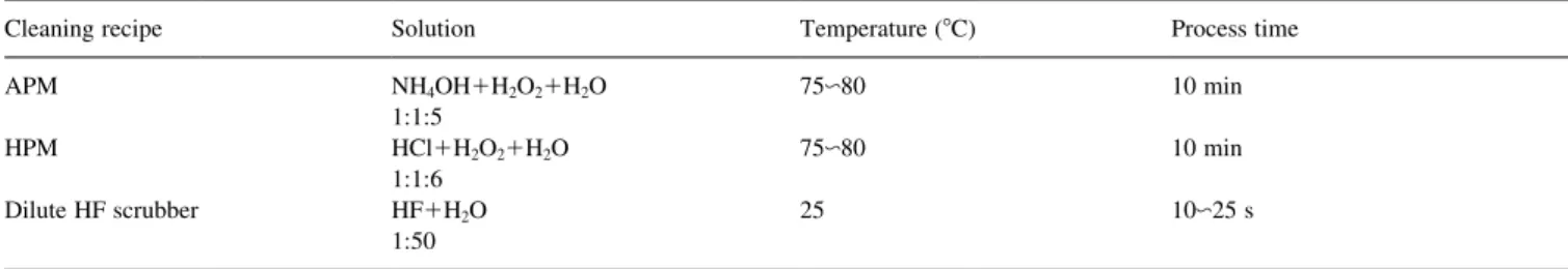
The conditions of the clean recipe
Cleaning recipe Solution Temperature (8C) Process time
APM NH4OH1H2O21H2O 75t80 10 min
1:1:5
HPM HCl1H2O21H2O 75t80 10 min
1:1:6
Dilute HF scrubber HF1H2O 25 10t25 s
1:50
Fig. 3. The relation between NH4OH ratio and particle removal ef®ciency.
Table 3
The clean effect for several combined cleaningsa
Clean recipe Defect (.0.2 mm) Oxide loss (A) Surface roughness by AFM (A) K Fe Ca Cu Mn APM1HF scrubber 5 s 47 13.4 3.14 2.31 1.15 3.84 1.07 1.62 APM1HF scrubber 15 s 19 37.4 3.43 2.79 1.07 3.38 1.08 ± APM1HF scrubber 30 s 8 74.2 4.85 3.14 1.21 3.24 0.98 ± HF scrubber 15s1APM 89 41.8 3.52 3.33 1.27 5.29 1.19 ± APM1HF scrubber 15 s1HPM 19 43.1 3.38 3.12 ± ± 0.92 ± APM1HF scrubber 15 s1APM1HPM 11 45.7 3.47 3.11 ± ± 1.01 ± Standard HF 15 s scrubber 24 39.5 2.92 3.07 ± 6.58 1.14 ± APM only 98 4.45 2.32 84 2.21 11.15 0.79 1.95
Fig. 4. The AFM picture of `APM1HF scrubber 15 s1HPM clean'.
value of SS-12 is about 12.5±13.5 caused by KOH. APM cleaning is important for the slurry particle removal due to the fact that both the slurry and wafer surface are have the same sign of zeta potential (negative). If a HF dip is imple-mented before APM, the surface will be positive and will gather the negative particle, such as silica. The defect will increase after the attraction occurs. From the above expla-nation of the zeta potential concept, it could explain the results of Table 2 why the sequence of `HF scrubber prior to APM' shows the worse defect level and metal than `APM prior to dilute HF scrubber'.
Implementation of the dilute HF will result in the etching of a thin layer of oxide ®lm. During the CMP process utiliz-ing SS-12 slurry, the metal ion of potassium can penetrate the oxide and nitride ®lm and become `trapped' in the damaged region caused by CMP. Using dilute HF to etch a thin oxide layer will result in the metal ions being carried away from the wafer surface. There is a signi®cant differ-ence between traditional RCA clean and post CMP cleaning due to the effect of changing the sequence of chemical cleaning steps. It has been widely accepted that a dilute HF cleaning prior to the APM cleaning can provide a very low metal and particle contamination [6]. However,
accord-ing to the results shown in Table 2, when the order of the dilute HF and APM steps are switched, particles and metal levels are decreased by approximately a factor of four or ®ve. It is believed that the challenge for post-CMP cleaning is to remove most of the residual slurry particles with the APM solution in the ®rst step. Then, once slurry particles are removed, the dilute HF in the second step is able to etch the top 30±50 AÊ of oxide, thereby removing the metallic contamination which has been incorporated in the surface and near surface region. Otherwise, if the HF dip is prior to the APM cleaning, the slurry particles cannot be easily removed during HF dip because the zeta potential between the materials is of different signs. The surface of wafer will gather the slurry particle and the surface region under the slurry particles are not etched and it can be dif®cult to remove metallic contamination with the following cleaning agents.
The HPM process will remove the sodium, calcium, ferric, aluminum and other metal ions. These ions may come from the polishing machine and slurry ¯ow system, such as polish pads, polish heads, wafer transfer system, diamond disc slurry piping and the slurry itself. This clean-ing step for improvclean-ing the solubility of metal ions results in
Y.L. Wang et al. / Thin Solid Films 332 (1998) 385±390 389
the formation of soluble complexes. In solution, the Cl2
anion is a highly reactive ion and may contribute to the removal of these metal ions. So the HPM cleaning is neces-sary to implement into the post CMP cleaning process.
The other sequence is evaluated in this study. Adding one step of APM before HPM to compare with the APM/HF scrubber 15 s/HPM process. From the results of Table 2, there is no signi®cant defect and metal ion removal due to the cleaning limitation.
5. Conclusions
The wafer surface is contaminated by particles and metal-lic ions during the CMP process. Since the planarization of STI is carried out within the device formation, it is of great importance to remove the residual particles and metallic impurities for improving device yield and performance. A new modi®ed multi-chemicals spray cleaning process for post STI CMP has been developed. This cleaning sequence provides a lower level defect and metallic contamination than the traditional post-CMP cleaning process. Besides, the addition of a dilute HF dip step to the post-STI CMP
process reduces potassium concentration and other defects signi®cantly. Further addition of HPM can reduce sodium, calcium, ferric and aluminum concentrations. Finally, a total cleaning formula: `APM1HF dip 15 s1HPM', is capable of removing virtually all major metallic ions down to below the detection limit of TXRF.
References
[1] N. Itoh, C. Yoshino, S. Matsuda, Y. Tsuboi, K. Inou, Y. Katsumata, H. Iwai, IEEE 1992, Bipolar Circuit and Technology Meeting, p. 104. [2] B. Davari, C.W. Koburger, R. Schulz, et al., IEDM Tech. Dig. (1998)
89.
[3] S.S. Cooperman, A.I. Nasr, G.L. Gyula, J. Electrochem. Soc. 142 (1995) 3180.
[4] I. Ali, M. Rodder, S.R. Roy, G. Shinn, M. Islam Raja, J. Electrochem. Soc. 142 (1995) 3088.
[5] L.J. Chen, Y.H Lee, C.C. Diao, T.H. Chen, G.G. Luo, J.H. Ho, Proc. 1st Int. Chemical-Mechanical Polish for VLSI/ULSI Multilevel Intercon-nection Conf., 1996, p. 307.
[6] W. Kern, D.A. Puotineu, Cleaning Solution Based on Hydrogen Perox-ide for Use in Semiconductor Technology, RCA Review, June 1970, p. 187.
[7] I.J. Malik, J. Zhang, A.J. Jensen, A Model Study for Post CMP Clean-ing, MRS ProceedClean-ing, Spring 1995.