IEEE ELECTRON DEVICE LETTERS, VOL. 32, NO. 2, FEBRUARY 2011 173
Novel Sub-10-nm Gate-All-Around Si Nanowire
Channel Poly-Si TFTs With Raised Source/Drain
Yi-Hsien Lu, Po-Yi Kuo, Member, IEEE, Yi-Hong Wu, Yi-Hsuan Chen, and Tien-Sheng Chao, Senior Member, IEEE
Abstract—We have successfully fabricated novel sub-10-nm gate-all-around Si nanowire (NW) poly-Si TFTs with raised source/drain structure (GAA RSDNW-TFTs). The Si NW dimen-sion is about 7 × 12 nm. A superior smooth elliptical shape is obtained, for the first time, in the category of poly-Si NW TFTs through the use of a novel fabrication process requiring no advanced lithographic tools. The GAA RSDNW-TFTs ex-hibit low supply gate voltage (3 V), steep subthreshold swing ∼99 mV/dec, and high ION/IOFF> 107 (VD= 1 V) without
hydrogen-related plasma treatments. Furthermore, the DIBL of GAA RSDNW-TFTs is well controlled. These improvements can be attributed to the 3-D gate controllability, raised S/D struc-ture, and sub-10-nm Si NW channel. These novel GAA RSDNW-TFTs are, thus, quite suitable for system-on-panel and 3-D IC applications.
Index Terms—Gate-all-around (GAA), nanowire (NW), poly-Si thin-film transistors (poly-Si TFTs), raised source/drain (S/D).
I. INTRODUCTION
R
ECENTLY, nonplanar device structures have been devel-oped for better gate electrostatic control of channel po-tential [1]–[4]. Among these, gate-all-around silicon nanowire (GAA Si NW) transistors are promising candidates for fu-ture CMOS devices due to their reduced short-channel effects [2], [3]. Applications of Si NW transistors include nanoscale CMOS [2], memories [5], light-emitting devices [6], large-area electronics [7], and sensors for sensing chemical or biological species [8], [9]. The fabrication processes of NWs are tradition-ally prepared by either top–down or bottom–up approaches [5]– [8]. The top–down approaches employ advanced lithographic tools like deep UV steppers or e-beam writer tools. By contrast, the bottom–up methods may suffer from the uncontrollability of structural parameters, such as the length and diameter of NWs. Recently, several NW TFTs structures have been proposed [10]–[13]. These NW TFTs primarily use parasitic structures that have the advantages of low cost and simple fabrication methods. However, several issues, including the nonuniform, asymmetric wire shape, and rough wire surface, require solu-tions. Therefore, these devices have to be fabricated withaddi-Manuscript received October 25, 2010; revised November 3, 2010; accepted November 5, 2010. Date of publication December 17, 2010; date of current version January 26, 2011. This work was supported by the National Science Council, Taiwan, under Contract NSC-97-2221-E-009-152-MY3. The review of this letter was arranged by Editor J. K. O. Sin.
The authors are with the Department of Electrophysics, National Chiao Tung University, Hsinchu 30010, Taiwan (e-mail: [email protected]).
Color versions of one or more of the figures in this letter are available online at http://ieeexplore.ieee.org.
Digital Object Identifier 10.1109/LED.2010.2093557
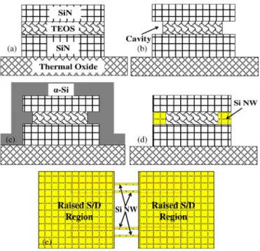
Fig. 1. (a)–(d) Key process flows of the GAA RSDNW-TFTs and (e) top view schematic structure after removing the dummy N/O/N.
tional treatments, such as hydrogen-related plasma treatments for more than 1 h, which improve the device characteristics. Furthermore, the thicknesses of thin n+ source/drain (S/D) in
conjunction with nanoscale NW will result in large parasitic resistance and poor driving currents. A nanoscale NW channel and a thick n+S/D region may not be satisfied simultaneously.
Therefore, a raised S/D structure is essential in an ideal GAA Si NW device.
In this letter, for the first time, novel sub-10-nm GAA Si NW poly-Si TFTs with raised S/D structure (GAA RSDNW-TFTs) are successfully fabricated and demonstrated. A su-perior smooth elliptical shape is obtained, for the first time, in the category of poly-Si NW TFTs through the use of a novel fabrication process. The proposed device simultaneously possesses sub-10-nm scaled Si NW and raised S/D without the use of advanced lithographic tools. The characteristics of GAA RSDNW-TFTs are superior and do not require hydrogen-related plasma treatments.
II. EXPERIMENT
The key process steps are shown in Fig. 1. The GAA RSDNW-TFTs were fabricated on Si wafers grown with a 500-nm thermal oxide layer. Si3N4/SiO2/Si3N4[N (70 nm)/O
(15 nm)/N (30 nm)] dummy sandwich structures were then
174 IEEE ELECTRON DEVICE LETTERS, VOL. 32, NO. 2, FEBRUARY 2011
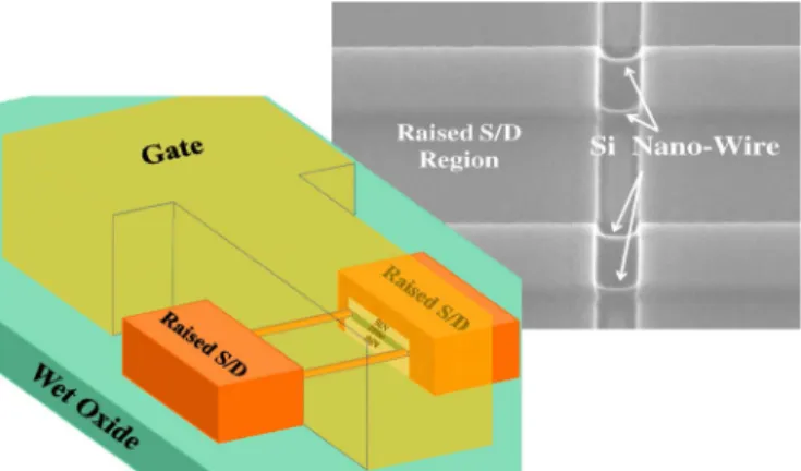
Fig. 2. Three-dimensional schematic structure of the multiple-channel GAA RSDNW-TFTs and SEM image of the structure formed after removing the dummy N/O/N.
deposited by low-pressure chemical vapor deposition (LPCVD) [Fig. 1(a)]. After the patterning and etching of NW definition region, lateral cavities in the N/O/N dummy sandwich struc-tures were formed by selective wet etching of the sandwiched oxide [Fig. 1(b)]. The clamped structure formed by the top and bottom nitride thus controls the shape of the lateral cavities quite well. After the formation of the lateral cavity, a 100-nm-thick amorphous Si (a-Si) layer was deposited by LPCVD at 500◦C [Fig. 1(c)], which formed the nanoscale Si NW and the raised S/D simultaneously. Next, the a-Si layer was crystallized by solid-phase crystallization (SPC) at 600◦C for 24 h in N2
ambient. The raised S/D region patterns were then defined by an I-line stepper. The raised S/D and the Si NW inlaid in the lateral cavities were fabricated by an anisotropic selective dry-etching step [Fig. 1(d)]. The Si NW channels with raised S/D were then selectively formed by removing the dummy N/O/N using hot phosphoric acid and dilute HF; top view was shown in Fig. 1(e). Fig. 2 shows the 3-D schematic structure of the multiple-channel GAA RSDNW-TFTs and the SEM image after removing the dummy N/O/N. A 7-nm LPCVD TEOS oxide and in situ doped n+ poly-Si gate with a thickness of
250 nm were then deposited. After the gate patterning, the raised S/D regions were implanted with arsenic (As+, 40-keV at 5× 1015-cm−2) and activated at 600 ◦C in an N2
ambi-ent. Conventional top gate planar-TFTs with 50-nm-thick SPC channel and TEOS gate oxide/poly-Si gate were also fabricated to serve as controls. All devices, for comparison, have identical gate lengths of 0.35 μm, and the channel width of planar-TFTs is 0.35 μm. After passivation and metallic processes, the GAA RSDNW-TFTs and planar-TFTs were fabricated without hydrogen-related plasma treatments.
III. RESULT ANDDISCUSSION
A cross-sectional transmission electron microscope (TEM) of a gate stacked GAA Si NW is shown in Fig. 3. The corner of Si NW was slightly etched during hot phosphoric acid process resulting in a smooth elliptical shape (about 7 × 12 nm), and the Si NW was surrounded by 7 nm of TEOS oxide and a poly-Si gate. A single crystalline cross-sectional view is observed in the Si NW. Fig. 4 shows the transfer charac-teristics of GAA RSDNW-TFTs and planar-TFTs. The GAA
Fig. 3. Cross-sectional TEM microphotograph of a gated stacked GAA Si NW. A single crystalline cross-sectional view is observed in the GAA Si NW.
Fig. 4. Transfer characteristics of GAA RSDNW-TFTs and planar-TFTs. The well-behaved transfer characteristics for the GAA RSDNW-TFTs without hydrogen-related plasma treatments are illustrated.
RSDNW-TFTs with a channel length of 0.35 μm (Nwire= 4,
effective width ∼0.03 × 4 = 0.12 μm) exhibit steeper swing, lower supply gate voltage, and higher ION/IOFFratio than the
planar-TFTs. It is believed that the electrical characteristics of poly-Si TFTs can be improved if the poly-Si grain size can be enhanced and the number of grain boundaries in the channel can be reduced. In this letter, a single crystalline cross-sectional view is observed in the sub-10-nm scaled Si NW. Thus, the probability of the channel region to cover a grain boundary in the width direction decreases resulted in significant reduction of the number of grain boundaries in Si NW. Although the Si NW is not single crystalline for all channel, the characteristics of the GAA RSDNW-TFTs without hydrogen-related plasma treatments are close to those of single-crystalline MOSFETs. Furthermore, the DIBL of the channels during device opera-tion of the GAA RSDNW-TFTs is negligible at VD= 2.5 V
(< 10 mV) due to the good gate controllability by the GAA structure and sub-10-nm Si NW channel. The surface-to-volume ratio results in higher performance on ION/IOFF, S.S.,
and DIBL as well.
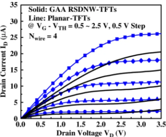
The output characteristics of the GAA RSDNW-TFTs and the planar-TFTs were compared in Fig. 5. In GAA RSDNW-TFTs, the saturation current (∼26.2 μA) improvement over the planar-TFT device (∼20.5 μA) is about 27% at VG− VTH= 2.5 V and VD= 3.5 V [width-normalized driving
cur-rent (218.3 μA/μm) is about 3.7 times that of the planar-TFTs (58.5 μA/μm)]. The GAA RSDNW-TFTs exhibit higher driv-ing currents than the planar-TFTs due to the raised S/D of the GAA RSDNW-TFTs (parasitic resistance Rp: 1.2 kΩ/5.78 kΩ
LU et al.: GATE-ALL-AROUND Si NANOWIRE CHANNEL POLY-Si TFTs WITH RAISED SOURCE/DRAIN 175
Fig. 5. Output characteristics of GAA RSDNW-TFTs and planar-TFTs, re-spectively. The RSDNW-TFTs exhibit higher driving and control well the floating-body effect.
TABLE I
COMPARISON OFSEVERALIMPORTANTPARAMETERS OF THEGAA RSDNW-TFTs WITHNW-TFTs INVESTIGATED INOTHERRESEARCH
for GAA RSDNW/planar-TFTs) [14]. In the planar-TFTs, the floating-body effects can be observed in output characteristics [14], [15]. These effects can be alleviated by either grounding the body with modified device structures or by using fully depleted SOI MOSFETs [16], [17]. The GAA RSDNW-TFTs exhibit kink-free output characteristics, indicating that the sub-10-nm Si NW channels are fully depleted by the GAA structure. In addition, we show a comparison of several important param-eters of the GAA RSDNW-TFTs with NW-TFTs investigated in other research [10]–[13] in Table I. We can observe a smooth elliptical shape of NW channel in our work. This is the first time that this has been realized in the category of poly-Si NW TFTs. Furthermore, GAA RSDNW-TFTs exhibit steeper S.S., high ION/IOFF, and lower supplied voltage
with-out NH3 plasma treatments. In contrast, the referenced
NW-TFTs require additional plasma treatments more than 1 h to enhance the performance of devices. The applied gate voltage is significantly reduced to 3 V, and the ION/IOFF> 107can be
achieved at VG = 3 V and VD= 1 V in GAA RSDNW-TFTs.
IV. CONCLUSION
Novel GAA Si NW TFTs with sub-10-nm Si NW and raised S/D structures have been successfully demonstrated. The GAA RSDNW-TFTs have steeper S.S., higher ION/IOFF, and
improved driving currents than planar-TFTs. The DIBL and floating-body effect were significantly suppressed due to the good gate controllability and fully depleted operation. This
combination of GAA gate stacked structure, raised S/D, and sub-10-nm NW channel appears to be promising for SOP and future monolithic 3-D IC applications.
ACKNOWLEDGMENT
The authors would like to thank the National Nano Device Laboratories and the Nano Facility Center of the National Chiao Tung University, Hsinchu, Taiwan, for the processes support.
REFERENCES
[1] B. Doyle, B. Boyanov, S. Datta, M. Doczy, S. Hareland, B. Jin, J. Kavalieros, T. Linton, R. Rios, and R. Chau, “Tri-gate fully-depleted CMOS transistors: Fabrication, design and layout,” in VLSI Symp. Tech.
Dig., 2003, pp. 133–134.
[2] J. Chen, T. Saraya, and T. Hiramoto, “Mobility enhancement over uni-versal mobility in (100) silicon nanowire gate-all-around MOSFETs with width and height of less than 10 nm range,” in VLSI Symp. Tech. Dig., 2010, pp. 175–176.
[3] J.-T. Park and J.-P. Colinge, “Multiple-gate SOI MOSFETs: Device de-sign guidelines,” IEEE Trans. Electron Devices, vol. 49, no. 12, pp. 2222– 2229, Dec. 2002.
[4] H. Lee, L.-E. Yu, S.-W. Ryu, J.-W. Han, K. Jeon, D.-Y. Jang, K.-H. Kim, J. Lee, J.-H. Kim, S. C. Jeon, G. S. Lee, J. S. Oh, Y. C. Park, W. H. Bae, H. M. Lee, J. M. Yang, J. J. Yoo, and Y.-K. Choi, “Sub-5 nm all around gate FinFET for ultimate scaling,” in VLSI Symp. Tech. Dig., 2006, pp. 58–59.
[5] X. Duan, Y. Huang, and C. M. Lieber, “Nonvolatile memory and pro-grammable logic from molecule-gated nanowires,” Nano Lett., vol. 2, no. 5, pp. 487–490, Apr. 2002.
[6] M. C. McAlpine, R. S. Friedman, S. Jin, K. Lin, W. U. Wang, and C. M. Lieber, “High-performance nanowire electronics and photonics on glass and plastic substrates,” Nano Lett., vol. 3, no. 11, pp. 1531–1535, Nov. 2003.
[7] X. Duan, C. Niu, V. Sahi, J. Chen, J. W. Parce, S. Empedocles, and J. L. Goldma, “High-performance thin-film transistors using semiconduc-tor nanowires and nanoribbons,” Nature, vol. 425, no. 6955, pp. 274–278, Sep. 2003.
[8] Y. Cui, Q. Wei, H. Park, and C. M. Lieber, “Nanowire nanosensors for highly sensitive and selective detection of biological and chemical species,” Science, vol. 293, no. 5533, pp. 1289–1292, Aug. 2001. [9] Z. Li, Y. Chen, X. Li, T. I. Kamins, K. Nauka, and R. S. Williams,
“Sequence-specific label-free DNA sensors based on silicon nanowires,”
Nano Lett., vol. 4, no. 2, pp. 245–247, Feb. 2004.
[10] Y.-C. Wu, T.-C. Chang, C.-W. Chou, Y.-C. Wu, P.-T. Liu, C.-H. Tu, J.-C. Lou, and C.-Y. Chang, “Effects of channel width and NH3plasma passivation on electrical characteristics of polysilicon thin-film transis-tors by pattern-dependent metal-induced lateral crystallization,” J.
Elec-trochem. Soc., vol. 152, no. 7, pp. G545–G549, 2005.
[11] H.-H. Hsu, H.-C. Lin, J.-F. Huang, and C.-J. Su, “Poly-Si nanowire thin-film transistors with inverse-T gate,” in Proc. Ext. Abstract SSDM, 2007, pp. 818–819.
[12] C.-J. Su, H.-C. Lin, H.-H. Tsai, H.-H. Hsu, T.-M. Wang, T.-Y. Huang, and W.-X. Ni, “Operations of poly-Si nanowire thin-film transistors with a multiple-gated configuration,” Nanotechnology, vol. 18, no. 21, pp. 1–7, May 2007.
[13] T.-C. Liao, S.-W. Tu, M. H. Yu, W.-K. Lin, C.-C. Liu, K.-J. Chang, Y.-H. Tai, and H.-C. Cheng, “Novel gate-all-around poly-Si TFTs with multiple nanowire channels,” IEEE Electron Device Lett., vol. 29, no. 8, pp. 889–891, Aug. 2008.
[14] P.-Y. Kuo, Y.-S. Huang, Y. H. Lue, T. S. Chao, and T. F. Lei, “The characteristics of n- and p-channel poly-Si thin-film transistors with fully Ni-salicided S/D and gate structure,” J. Electrochem. Soc., vol. 157, no. 1, pp. H113–H119, 2010.
[15] M. Valdinoci, L. Colalongo, G. Baccarani, G. Fortunato, A. Pecora, and I. Policicchio, “Floating body effects in polysilicon thin-film transistors,”
IEEE Trans. Electron Devices, vol. 44, no. 12, pp. 2234–2241, Dec. 1997.
[16] F. Silveira, D. Flandre, and P. G. A. Jespers, “A gm/IDmethodology for
the design of CMOS analog circuits and its application to the synthesis of a silicon-on-insulator micropower OTA,” IEEE J. Solid-State Circuits, vol. 31, no. 9, pp. 1314–1319, Sep. 1996.
[17] J. P. Colinge, “Thin-film, accumulation-mode p-channel SOI MOSFETs,”
![TraditionalMLCalgorithmsmainlytacklethebatchMLCproblem,wheretheinputdataarepresentedinabatch[24,28].Nevertheless,inmanyMLCapplicationssuchase-mailcategorization[22],multi-labelexamplesarriveasastream.Onlineanalysisistherefore dimensionreducermotivatedbyma](data:image/gif;base64,R0lGODlhAQABAIAAAP///wAAACH5BAEAAAAALAAAAAABAAEAAAICRAEAOw==)