A characterization on emission property of In
2
O
3
–SiO
2
nanocomposite thin
films
Yang-Ru Lyu, Tsung-Eong Hsieh
⁎
Department of Materials Science and Engineering, National Chiao Tung University, Hsinchu, 30010, Taiwan, ROC
a b s t r a c t
a r t i c l e i n f o
Available online 18 June 2012 Keywords:
In2O3 Nanocomposite Photoluminescence Emission mechanisms
Nanocomposite thinfilms containing finely dispersed, crystalline In2O3nanoparticles embedded in SiO2
ma-trix were fabricated by target-attachment sputtering method. Transmission electron microscopy observed single crystalline In2O3nanoparticles uniformly embedded in SiO2matrix of the samples with In2O3content
less than about 60 vol.%. Photoluminescence spectra of the In2O3–SiO2nanocomposite samples were found to
comprise of the blue, green and red emissions. Analytical results indicated that the red and green emissions are correlated to the transitions from conduction band (CB) edge to the Ini•••and V‴Indefect levels,
respective-ly, while the blue emission is originated from the transition from CB edge to VO••level or from VO•level to the
valence band edge.
© 2012 Elsevier B.V. All rights reserved.
1. Introduction
As a well-known wide bandgap (Eg) semiconductor, indium oxide
(In2O3; Eg= 3.75 eV) recently attracts numerous attentions in
opto-electronic applications owing to its high electrical conductivity and high transparency in visible-light wavelength range[1,2]. One of the attractive properties of In2O3 is its strong visible-light
photo-luminescence (PL). Lee et al. reported the PL signal at 637 nm from the In2O3 thin films [3]. Mazzera et al. observed three emission
bands separately located at 454, 563 and 631 nm in the cat-hodoluminescence spectra of In2O3 samples[4]. The correlation of
In2O3emissions to oxygen vacancy has been separately discussed by
Liang et al.[5]and Ko et al.[6]. They ascribed the emissions in the blue-green and blue-red regions to the presence of oxygen vacancies in In2O3. Furthermore, broad PL peaks at 416 and 435 nm from In2O3
nanowires were observed by Wu et al.[7]. Guha et al. found a blue-green PL emission in the In2O3nanopyramid and nanocolumn
sam-ples[8]. Their studies also reported the correlations of luminescence property to oxygen defects in In2O3.
Strong UV emission that resulted from the direct bandgap transi-tion in In2O3has been reported by Murali et al.[9]and Seo et al.
[10], respectively. However, the correlation of emissions to the transi-tions in between the defect levels of In2O3-based samples remains
ob-scure since the experimental data rarely illustrated the defect-level transitions in a straightforward manner. As reported previously [5–8], a wide range of emissions in visible-light wavelength range has been ascribed to the oxygen vacancies in In2O3. This might be
in-appropriate since the oxygen defect levels unlikely split in such a wide range in the bandgap of In2O3. As a result, a clarification on
the emission mechanisms corresponding to the defect-level transi-tions in In2O3is required.
This work prepares the nanocomposite thinfilms comprised of In2O3nanoparticles embedded in SiO2matrix by utilizing the
target-attachment sputtering method[11,12]. Characterizations of PL emis-sions, microstructures and compositions of the nanocomposite sam-ples containing various sizes and amounts of In2O3nanoparticles are
presented. Accordingly, the PL properties correlated to the defect-level transitions of emissions in nanocomposite thinfilms containing In2O3nanoparticles are discussed.
2. Experimental details
The In2O3–SiO2nanocomposite thinfilms were deposited on Si wafer
substrates by the target-attachment method in a sputtering system with the background pressure better than 10−7Torr. Appropriate amounts of In2O3pellets were mounted on a 3-inch quartz target and the
radio-frequency (RF) magnetron sputtering deposition was carried out at the working pressure of 3.5 mTorr with argon (Ar) as the inlet gasflow. The sizes and densities of In2O3nanoparticles in the nanocomposite
thinfilms were adjusted by varying the sputtering power and the num-ber of In2O3pellets.Table 1lists the sample designation established in
terms of the sputtering deposition conditions. Characterizations of PL emissions, microstructures and compositions of the samples were imme-diately followed after the completion of sample preparation without per-forming the post annealing treatment. PL spectra were measured at room temperature in the wavelength range of 350 to 750 nm using a self-assembly PL apparatus equipped with a 325 nm He–Cd laser. Micro-structures of nanocomposite thinfilms were characterized by transmis-sion electron microscopy (TEM; JEOL JEM-2100F) operating at 200 kV. Evolution of chemical bonds in the samples was examined by X-ray pho-toemission spectroscopy (XPS; American Physical Electronics ESCA PHI 1600) using the Mg-KαX-ray excitation.
⁎ Corresponding author. Tel.: +886 3 5712121x55306; fax: +886 3 5724727. E-mail address:[email protected](T-E. Hsieh).
0257-8972/$– see front matter © 2012 Elsevier B.V. All rights reserved.
doi:10.1016/j.surfcoat.2012.06.037
Contents lists available atScienceDirect
Surface & Coatings Technology
j o u r n a l h o m e p a g e : w w w . e l s e v i e r . c o m / l o c a t e / s u r f c o a t3. Results and discussion 3.1. Microstructure characterization
Fig. 1(a)–(e) presents the TEM micrographs of various In2O3–SiO2
nanocomposite thinfilms prepared in this study. Attached in the upper right-hand corners ofFig. 1(a)–(c) are the enlarged images of In2O3nanoparticles embedded in those nanocomposite samples. The
lattice fringes decorating in the In2O3 nanoparticles indicate that
each of them corresponds to a single crystalline particle. However, those lattice fringes became difficult to be observed in samples g and i (Fig. 1(d) and (e)) due to their high In2O3contents that the
im-ages of nanoparticles severely overlap when projected on the TEM screen. Representative selected area electron diffraction (SAED) of sample shown inFig. 1(f) indicates that the embedded In2O3phase
is body-centered-cubic (BCC) structure according to the Joint Com-mittee of Powder Diffraction Standards (JCPDS) No. 06-0416. The av-erage particle sizes were obtained by measuring the sizes of at least 60 In2O3nanoparticles in the TEM images for each of the samples
and the results are summarized inTable 1.
3.2. XPS analysis
Fig. 2(a) depicts the In 3d XPS spectra of nanocomposite samples which indicate that all samples contain the sole In2O3phase without
the presence of metallic In (443.56 eV[13]). A monotonic increase in intensities of In 3d XPS peaks can be observed in samples a to j with the increase of In2O3 pellet-to-target area coverage ratio and RF
sputtering power. Moreover, the binding energies corresponding to In 3d3/2and In 3d5/2XPS peaks shown inFig. 2(a) are separately
equal to 452.43 ± 0.10 eV and 444.83 ± 0.10 eV, which are in agree-ment with the reported values for In\O bond [14]. We note that XPS spectra shown inFig. 2(a) were also adopted to calibrate the In2O3 contents in the samples and the results were presented in
terms of the volume ratios of In2O3in the samples as listed inTable 1.
The O 1s XPS spectra shown inFig. 2(b) reveal, with the increase of In2O3 pellet-to-target area coverage ratio and RF sputtering
power, the XPS peak shifts toward the high binding energy side and the asymmetries of XPS peaks become apparent for the samples with high In2O3contents. According to Dupin et al.[15], the status
of oxygen defects in oxide systems could be distinguished by analyz-ing the O 1s XPS profiles. With the aid of the de-convolution of XPS spectra, the roles of various oxygen defects in the shift and asymme-try of O 1s XPS profiles shown inFig. 2(b) can be clarified.
Curvefitting results of O 1s XPS spectra for samples are summa-rized inTable 2. Three different oxygen defect species present in the nanocomposite samples: Olattice, O−, and O2−separately represent
the lattice oxygen in In2O3 lattice (~ 530.2 eV), the oxygen ions at
the nanoparticle surface (~531.8 eV), and the loosely bound oxygen in the amorphous SiO2or partially weakly adsorbed oxygen species
(~532.7 eV)[11]. The O−ions were generated on nanoparticle sur-face during the sputtering as reported by Chen et al.[16]. Moreover, the content of Olatticecomponent increases from 5.91 to 14.36% for
samples a to j. This is ascribed to the increases of In2O3content in
nanocomposite layer since the Olattice signal is correlated to the
In\O bond. Note that the variation of Olatticecomponent deduced
from XPS profiles allows us to estimate the deviation of stoichiomet-ric ratio for In2O3phase in each of the samples. The results obtained
will be discussed in conjunction of the PL properties to identify the emission mechanism of In2O3.
3.3. Photoluminance property and origins of emissions
Fig. 3presents the PL spectra of nanocomposite samples a–j. We note that the PL intensity decreases with the increase of In2O3content
of the sample. According to the TEM images shown inFig. 1(d) and (e), high In2O3content results in the coalescence of nanoparticles
and, hence, the luminescence property of such nanocomposite thin films becomes a resemblance to that of In2O3bulk which is known
to emit no visible light at room temperature[17]. All PL spectra can be de-convoluted into red, green and blue emissions; the peak positions and integrated intensity ratios of emissions deduced from the PL curve fitting results are summarized inTable 2. Since Eg= 3.75 eV (~330 nm)
for In2O3which is located at the UV regime, those de-convoluted PL
emissions were hence correlated to the carrier recombination in be-tween the conduction band (CB) edge and the defect levels and/or the defect levels and the valence band (VB) edge. Moreover, although there were slight shifts of emission peaks due to weak confinement ef-fect, the quantum confinement effect on PL property is negligible since the sizes of In2O3nanoparticles prepared in this study are larger than
the Bohr radius of In2O3(=2.14 nm)[5]. As a result, the PL data
pres-ented in this study are appropriate for characterizing the mechanisms of visible-light emissions of In2O3–SiO2nanocomposite thinfilms.
Previous studies reported several possible defect types in In2O3,
e.g., oxygen vacancy (VO••), indium interstitial (Ini•••) and indium
va-cancy (V‴In)[4,10]. Due to its relatively large size (0.138 nm), oxygen
interstitial (O″i) is unlikely present in our samples and hence it is
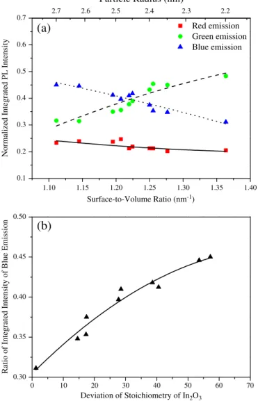
aborted in the following discussion[4]. Correlations of visible-light emissions to interface features of the samples have been reported in several systems containing wide-bandgap semiconductors [18–22] and strong emission was observed in the nanocomposite samples with high specific-surface-area (SSA) properties.Fig. 4(a) presents the normalized integrated intensities of the blue, green and red emis-sions as a function of the surface-to-volume ratio and particle radius of In2O3nanoparticles. It was found that the intensity ratios of blue
and red emissions decrease with the increase of surface-to-volume ratio and vice versa for green emission. This indicates that those emis-sions may result from different carrier recombination processes in nanocomposite samples. It is well known that, with the shrinkage of particle size, the band bending effects at the particle surface become obvious[23,24]. Accordingly, the surface states are created due to the holes migrating toward the particle surface while the volume states are generated owing to the electron migrating into the bulk of particle. According to trends depicted inFig. 4(a), it can be conclud-ed that the rconclud-ed and blue emissions are associatconclud-ed with the donor de-fects whereas the green emission is correlated to the acceptor dede-fects in In2O3nanoparticles. For Ini•••, it should act as a donor level more
close to CB edge in comparison with VO••and, hence, the transition
from CB edge to Ini•••defect level is most likely correlated to the red
emission. This is in agreement with that reported by Kumar et al. who proposed that the presence of Ini••• in In2O3 is responsible to
the red emission[25].
As to the green and blue emissions, they are commonly related to the presence of oxygen deficiencies in the samples[7,10,26]. Nevertheless, Table 1
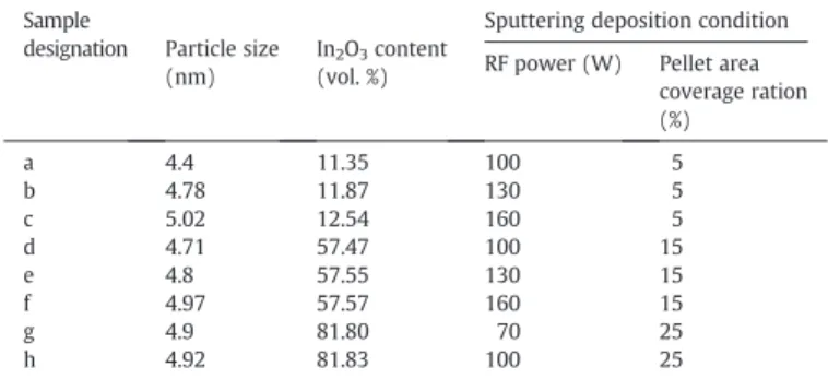
A list of In2O3nanoparticle sizes, In2O3contents and sputtering deposition conditions of nanocomposite samples.
Sample
designation Particle size (nm)
In2O3content (vol. %)
Sputtering deposition condition RF power (W) Pellet area
coverage ration (%) a 4.4 11.35 100 5 b 4.78 11.87 130 5 c 5.02 12.54 160 5 d 4.71 57.47 100 15 e 4.8 57.55 130 15 f 4.97 57.57 160 15 g 4.9 81.80 70 25 h 4.92 81.83 100 25
experimental evidences to verify such a correlation remain insufficient [27,28]. For instance, Wu et al. ascribed the green emission of In2O3to
the oxygen vacancies (VOX) and In\O vacancy complex (VIn,VO)X[7].
However, the shallow donor level generated by VOXis not well identified.
The plots shown inFig. 4(a) indicate that the green and blue emissions are separately related to the acceptor defect level and the donor defect level. Among the possible acceptor defects in In2O3, i.e., V′In, V″Inand V
‴In, the green emission is hence correlated to the transition from CB
edge or shallow donor levels to the V‴Insince it is a plausible defect
type in In2O3in accord with the Frenkel disorder reaction InIn→Ini•••+
V‴In.
Blue emission is another visible emission that has been attributed to the presence of oxygen defects in the samples[5,6].Fig. 4(a) indicates, similarly to the red emission, such an emission also relies on the transi-tion relating to donor levels in the samples. According to relative amounts of Olatticecomponent deduced from XPS profiles, we calculated
the deviations of stoichiometry for In2O3(i.e., In:O= 2:3) in order to
es-timate the amount of oxygen defects in In2O3nanoparticles of various
Fig. 1. (a) to (e) show the TEM micrographs corresponding to samples a, b, e, g and i. Attached at the upper right-hand corners of (a) to (c) are the high-magnification images of In2O3nanoparticles. (f) is a typical SAED pattern taken from the nanocomposite sample.
samples.Fig. 4(b) plots the normalized integrated intensity of blue emission against the deviation of stoichiometry for In2O3nanoparticles.
Apparently, the increase of non-stoichiometry in In2O3amplifies the
blue emission, illustrating that the presence of oxygen defects in In2O3
nanoparticles is highly correlated to such an emission. However, oxygen defects include singly ionized VO•and doubly ionized VO••in many oxides.
Electron paramagnetic resonance (EPR) analysis on In2O3[4,25]and
several previous studies[29,30]have ascribed the blue emission to VO•.
Although VO••could not be detected due to its non-paramagnetic feature,
VO••might form via the hole trapping process, i.e., VO•+ h→VO••. Since the
relative populations of VO• and VO••defects could not be distinguished in
the present study, it is inferred that both the VO• and VO••donor levels
are correlated to the blue emission. That is, in accord with the possible energy levels in bandgap diagram, the blue emission might result from the transition from CB edge to VO••level and/or the transition
from VO• level and VB edge.
In accord with above discussions, the plausible defect energy levels corresponding to the red, green and blue emissions in bandgap diagram of In2O3are constructed and delineated inFig. 5. We hope
that the analytical results presented in this study would benefit the
(a)
In 3d
3d3/2
3d5/2
Binding Energy (eV)
Intensity (a.u.) j i h g f e d c b a 455.0 452.5 450.0 447.5 445.0 442.5 440.0 538 536 534 532 530 528 526
Binding Energy (eV)
Intensity (a.u.) 1s
(b)
O 1s
j i h g f e d c b aFig. 2. (a) In 3d and (b) O 1s XPS spectra of In2O3–SiO2nanocomposite samples.
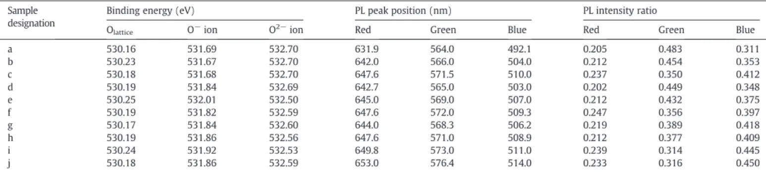
Table 2
Summary of XPS and PL curvefitting results for In2O3–SiO2nanocomposite samples and the integrated PL intensity ratios of visible-light emissions deduced from the PL curvefitting. Sample
designation
Binding energy (eV) PL peak position (nm) PL intensity ratio
Olattice O−ion O2−ion Red Green Blue Red Green Blue
a 530.16 531.69 532.70 631.9 564.0 492.1 0.205 0.483 0.311 b 530.23 531.67 532.70 642.0 566.0 504.0 0.212 0.454 0.353 c 530.18 531.68 532.70 647.6 571.5 510.0 0.237 0.350 0.412 d 530.19 531.84 532.69 642.7 565.0 503.0 0.202 0.449 0.348 e 530.25 532.01 532.50 645.0 569.0 507.0 0.212 0.432 0.375 f 530.19 531.82 532.59 647.6 572.0 509.3 0.247 0.356 0.397 g 530.17 531.84 532.60 644.0 568.3 506.2 0.219 0.389 0.418 h 530.19 531.86 532.56 647.6 571.0 508.9 0.212 0.377 0.409 i 530.24 531.92 532.53 649.8 573.0 511.0 0.239 0.314 0.445 j 530.18 531.86 532.59 653.0 576.4 514.0 0.233 0.316 0.450 300 400 500 600 700 800 900 1000 1100 1200 1300 1400 a b c d e
(a)
Wavelength (nm) Photoluminescence Intensity 350 400 450 500 550 600 650 700 750 Wavelength (nm) 350 400 450 500 550 600 650 700 750 420 440 460 480 500 520 f g h i j(b)
Photoluminescence Intensityunderstanding on the emission properties and their correlations to defect configuration of nano-scale In2O3.
4. Conclusions
The In2O3–SiO2nanocompositefilms containing In2O3nanoparticles
were fabricated by target-attachment sputtering and their visible-light emission mechanisms were analyzed. Single crystalline In2O3
nanoparticles uniformly dispersed in SiO2 matrix were observed by
TEM in the samples with In2O3content less than about 60 vol.%. XPS
analysis revealed that the main oxygen defect type associated with In2O3nanoparticles is the O−ions residing on their surfaces due to the
large SSA feature of nanoparticles. The PL spectra of the In2O3–SiO2
nanocomposite thinfilms were found to comprise of blue, green, and red emissions. Since the direct bandgap transition of In2O3is located at
the UV regime and the quantum confinement effect is negligible in this study, those visible-light emissions are hence associated to the de-fect level transitions in bandgap of In2O3. In accord with the
character-izations on luminance property, microstructures and composition of nanocomposite samples, the red emission is correlated with the transi-tion from CB edge to Ini•••donor level, the green emission is originated
from the transition from CB edge or shallow donor levels to the V‴In
ac-ceptor level and the blue emission is resulted from the transition from CB edge to VO••level and/or the transition from VO• level and VB edge.
Accordingly, the defect energy levels corresponding to the visible-light emissions in bandgap diagram of In2O3was established in order to
elu-cidate the luminance mechanisms of In2O3–SiO2nanocomposite thin
films.
Acknowledgments
This work is supported by National Science Council (NSC), Taiwan, ROC, under the contract no. NSC98-2221-E-009-037-MY2. The assis-tance of TEM analysis provided by Mr. Wei-Lin Wang in the Depart-ment of Materials Science and Engineering, National Chiao Tung University, Taiwan, ROC, is also deeply acknowledged.
References
[1] R.A. Sailer, A. Wagner, C. Schmit, N. Klaverkamp, D.L. Schulz, Surf. Coat. Technol. 203 (2008) 835.
[2] Y. Shigesato, S. Takaki, T. Haranoh, J. Appl. Phys. 71 (1992) 3356.
[3] M.S. Lee, W.C. Choi, E.K. Kim, C.K. Kim, S.K. Min, Thin Solid Films 279 (1996) 1. [4] M. Mazzera, M. Zha, D. Calestani, A. Zappettini, L. Lazzarini, G. Salviati, L. Zanotti,
Nanotechnology 18 (2007) 355707.
[5] C.H. Liang, G.W. Meng, Y. Lei, F. Phillip, L.D. Zhang, Adv. Mater. 13 (2001) 1330. [6] T.S. Ko, C.P. Chu, J.R. Chen, T.C. Lu, H.C. Kuo, S.C. Wang, J. Cryst. Growth 310 (2008)
2264.
[7] X.C. Wu, J.M. Hong, Z.J. Han, Y.R. Tao, Chem. Phys. Lett. 373 (2003) 28. [8] P. Guha, S. Kar, S. Choudhari, Appl. Phys. Lett. 85 (2004) 3851.
[9] A. Murali, A. Barve, V.J. Leppert, S.H. Risbud, I.M. Kennedy, H.W.H. Lee, Nano Lett. 1 (2001) 287.
[10] W.S. Seo, H.H. Jo, K. Lee, J.T. Park, Adv. Mater. 15 (2003) 795. [11] Y.Y. Peng, T.E. Hsieh, C.H. Hsu, Nanotechnology 16 (2005) 1. [12] Y.Y. Peng, T.E. Hsieh, Appl. Phys. Lett. 89 (2006) 211909-1. [13] R.W. Hewitt, N. Winograd, J. Appl. Phys. 51 (1980) 2620.
[14] A. Gurlo, M. Ivanovskaya, A. Pfau, U. Weimar, W. Gopel, Thin Solid Films 307 (1997) 288.
[15] J.C. Dupin, D. Gonbeau, P. Vinatier, A. Levasseur, Phys. Chem. Chem. Phys. 2 (2000) 1319.
[16] M. Chen, X. Wang, Y.H. Yu, Z.L. Pei, X.D. Bai, C. Sun, R.F. Huang, L.S. Wen, Appl. Surf. Sci. 158 (2000) 134.
[17] Y. Ohhata, F. Shinoki, S. Yoshida, Thin Solid Films 59 (1979) 255.
[18] S. Chakrabarti, D. Ganguli, S. Chaudhuri, J. Phys. D: Appl. Phys. 36 (2003) 146. [19] L.I. Burova, D.I. Petukhov, A.A. Eliseev, A.V. Lukashin, Y.D. Tretyakov, Superlattices
Microstruct. 39 (2006) 257.
[20] B. Damilano, N. Grandjean, F. Semond, J. Massies, M. Leroux, Appl. Phys. Lett. 75 (1999) 962.
[21] Y.G. Cao, X.L. Chen, Y.C. Lan, J.Y. Li, Y.P. Xu, T. Xu, Q.L. Liu, J.K. Liang, J. Cryst. Growth 213 (2000) 198.
[22] S.T. Selvan, C. Bullen, M. Ashokkumar, P. Mulvaney, Adv. Mater. 13 (2001) 985. [23] Y.J. Lee, J.L. Gary, In: IEEE Photo. Spec. Conf., Hawaii, 1994, p. 287.
[24] H.H. Mueller, M.J. Schulz, IEEE Trans. Electron Devices 44 (1997) 1539. [25] M. Kumar, V.N. Singh, F. Singh, K.V. Lakshmi, B.R. Mehta, J.P. Singh, Appl. Phys.
Lett. 92 (2008) 171907-1.
[26] M.J. Zheng, L.D. Zhang, G.H. Li, X.Y. Zhang, X.F. Wang, Appl. Phys. Lett. 79 (2001) 839.
[27] G. Wang, J. Park, D. Wexler, M.S. Park, J.H. Ahn, Inorg. Chem. Commun. 46 (2007) 4778.
[28] Y. Li, w. Cai, G. Duan, F. Sun, B. Cao, F. Lu, Q. Fang, I.W. Boyd, Appl. Phys. A 81 (2005) 269.
[29] Y. Zhao, Z. Zhang, Z. Wu, H. Dang, Langmuir 20 (2004) 27.
[30] X.P. Shen, H.J. Liu, X. Fan, Y. Jiang, J.M. Hong, Z. Xu, J. Cryst. Growth 276 (2005) 471. 0.1 0.2 0.3 0.4 0.5 0.6 0.7
(a)
Normalized Integrated PL Intensity
Surface-to-Volume Ratio (nm-1) Red emission Green emission Blue emission 2.7 2.6 2.5 2.4 2.3 2.2
Particle Radius (nm)
1.10 1.15 1.20 1.25 1.30 1.35 1.40 0 10 20 30 40 50 60 70 0.30 0.35 0.40 0.45 0.50(b)
Ratio of Integrated Intensity of Blue Emission
Deviation of Stoichiometry of In2O3
Fig. 4. Normalized integrated intensity of (a) visible-light emissions as a function of surface-to-volume ratio and sizes of In2O3nanoparticles and (b) the ratio of integrated intensity of blue emission against the deviation of stoichiometry for In2O3.
Fig. 5. Schematic illustration of bandgap diagram of In2O3with the defect energy levels. The transitions corresponding to the red, green and blue emissions are indicated by the colored arrow lines in the plot.