shown that the axial ratio could be increased to about 25% and with symmetrical radiation pattern across the 3-dB AR band. Extensive study for the subarrays is in progress and will be reported later.
4. CONCLUSION
A single-fed elliptical dielectric resonator antenna designed for circular polarization has been presented. The elliptical dielectric resonator was excited by either a probe or a narrow aperture. The aperture fed elliptical CP DRA exhibited good CP performance when the dielectric resonator was rotated by 45° with respect to the major axis and with the elliptic cross-section aspect ratio of 1.5. The radiation patterns of the DRA excited by an aperture are symmetric in the broadside direction.
ACKNOWLEDGMENT
One of the authors, Steven Yang, appreciates the Department of Electrical Engineering and the Center for Applied Electromagnetic System Research of the University of Mississippi for providing the fabrication and measurement facilities.
REFERENCES
1. K.W. Leung, W.C. Wong, K.M. Luk, and E.K.N. Yung, Circular-polarised dielectric resonator antenna excited by dual conformal strips, Electron Lett 36 (2000), 484 – 486.
2. G. Drossos, Z. Wu, and L.E. Davis, Circular polarised cylindrical dielectric resonator antenna, Electron Lett 32 (1996), 281–283. 3. C.-Y. Huang, J.-Y. Wu, and K.-L. Wong, Cross-slot-coupled
micros-trip antenna and dielectric resonator antenna for circular polarization, IEEE Trans Antennas Propag 47 (1999), 605– 609.
4. K.W. Leung, Circularly polarized dielectric resonator antenna excited by a shorted annular slot with a backing cavity, IEEE Trans Antennas Propag 52 (2004), 765–2770.
5. K.W. Leung H.K. Ng, The slot-coupled hemispherical dielectric res-onator antenna with a parasitic patch: Applications to the circularly polarized antenna and wide-band antenna, IEEE Trans Antennas Propag 53 (2005), 1762–1769.
6. K.W. Leung, H.K. Ng, Theory and experiment of circularly polarized dielectric resonator antenna with a parasitic patch, IEEE Trans Anten-nas Propag 51 (2005), 405– 412.
7. A. Petosa, A. Ittipiboon, and M. Cuhaci, Array of circular-polarised cross dielectric resonator antennas, Electron Lett 32 (1996), 1742– 1743.
8. M.T.K. Tam and R.D. Murch, Circularly polarized circular sector dielectric resonator antenna, IEEE Trans Antennas Propag 48 (2000), 126 –128.
9. A.A. Kishk, An elliptic dielectric resonator antenna designed for circular polarization with single feed, Microwave Opt Technol Lett 37 (2003), 454 – 456.
10. Ansoft HFSS 9.2, Ansoft Corporation, Pittsburgh, PA, USA. 11. A.A. Kishk, Performance of planar four-element array of single-fed
circularly polarized dielectric resonator antenna, Microwave Opt Technol Lett 38 (2003), 381–384.
© 2006 Wiley Periodicals, Inc.
A 2.4, 5.2, AND 5.7 GHz CMFB
GILBERT DOWNCONVERTER WITH
LOW-VOLTAGE CASCODE CURRENT
MIRROR INPUT STAGE
Sheng-Che Tseng,1Chinchun Meng,1and Guo-Wei Huang2
1Department of Communication Engineering
National Chiao Tung University Hsinchu 300, Taiwan, Republic of China
2National Nanometer Device Laboratories
Hsinchu 300, Taiwan, Republic of China Received 4 April 2006
ABSTRACT: A triple-band (2.4, 5.2, and 5.7 GHz) CMFB downcon-version micromixer with a low-voltage cascode current mirror RF input stage has been demonstrated by the 0.18-m CMOS technology in this letter. Micromixer has a single-ended RF input stage, the CMFB topol-ogy is adopted to improve the conversion gain, and a differential-to-single output buffer is used to convert the differential output of the mixer into a single-ended output. The fully integrated downconversion micromixer has the conversion gain of 12 dB, LO-to-IF isolation of 43 dB, LO-to-RF isolation of 48 dB, and RF-to-IF isolation of 18 dB at 2.4 GHz. The mixer has the conversion gain of 7.5 dB, LO-to-IF isola-tion of 54 dB, LO-to-RF isolaisola-tion of 49.5 dB, and RF-to-IF isolaisola-tion of 25 dB at 5.7 GHz. The total quiescent current consumption of the circuit is 7.6 mA. © 2006 Wiley Periodicals, Inc. Microwave Opt Technol Lett 48: 2345–2349, 2006; Published online in Wiley Inter-Science (www.interscience.wiley.com). DOI 10.1002/mop.21950 Key words: Gilbert mixer; micromixer; CMFB; downconverter; RFIC
1. INTRODUCTION
Wireless communication has advanced swiftly and the age of the multiband transceiver such as wireless LAN 802.11a/b/g combo transceiver is coming. The large demand pursues the CMOS inte-gration of RF, analog, and digital blocks under consideration of the cost and yield. The bottleneck is the RF circuit integration in CMOS technology. In this paper, a wideband CMOS mixer, which could work with the low voltage supply of 1.8 V is designed at triple bands, that is, 2.4, 5.2, and 5.7 GHz.
A conventional double balanced Gilbert mixer can provide excellent port-to-port isolation by balanced operation [1]. Good common mode rejection is needed to preserve the excellent isola-tion in a Gilbert mixer, if the balanced signals are absent. How-ever, the common mode rejection provided by the biased current source deteriorates rapidly at high frequencies [2]. Thus, we adopted a Gilbert micromixer that can provide high speed response and eliminates the need for common rejection [3], but the DC current balance of the micromixer would influence isolation deeply. In this work, a micromixer was designed with a low-voltage cascode current mirror, which can achieve a truly balanced operation. Furthermore, active PMOS loads are used to improve the conversion gain and a differential-to-single output buffer is used to facilitate the on-wafer RF measurements.
2. CIRCUIT DESIGN
The circuit schematic of the CMFB (Common Mode Feedback) downconversion mixer is shown in Figure 1. The RF input stage is illustrated in Figure 2. It is a transconductance amplifier to generate a differential current by a common-gate-configured M5and a common-source-configured M2. A low-voltage cascode current mirror is adopted to keep the drain voltage of M2the same as that of M1. This low-voltage cascode current mirror can produce a pair of truly bal-anced DC currents because of the cascode configuration [4]. Thus, the
mixer has more balanced DC bias currents. There is no unbalanced DC signals to mix with the LO signal and this mixer can achieve high LO-to-IF isolation [5]. However, there would be five cascode tran-sistors with only a 1.8-V supply. Because of using a low-voltage cascode current mirror, this mixer could work with low voltage [6]. A common-gate-biased M5 and a common-source-biased M2 with a wide-swing cascode current mirror form an RF input transconductance stage, as shown in Figure 2. M5and M2provide equal magnitude, but out-of-phase transconductance gain, and hence, the RF input transconductance stage converts a single input voltage signal to differential current signals [7]. The RF input resistance can be derived as
Rin⫽
1
gm1/ /
1
gm5. (1)
Thus, the mixer can be designed to achieve wideband impedance matching. The common-gate-configured M5 possesses good fre-quency response, while the speed of common-source-configured M2is improved drastically by loading low input impedance at the input of common-source-configured M2.
The output current of this stage can be expressed as
Ia⫽ IDC1⫺ gm5RF (2)
Ib⫽ IDC2⫹ gm2RF,
where Iaand Ibare the drain current of M5and M6, respectively; IDC1and IDC2are quiescent current of M1and M2, respectively;
gm5and gm2are the transconductance of M5and M2, respectively.
With the assumption that the Gilbert cell is a perfect match, the differential current output of mixer can be derived as
IO⫽
冋
1
2共LOc⫹ LOd兲Ib⫹
1
2共LOc⫺ LOd兲Ia
册
Figure 1 Circuit schematic of the Gilbert downconverter with cascode current mirror RF input stage
Figure 2 RF input stage with a wide-swing cascode current mirror
Figure 3 Photograph of the Gilbert downconverter with cascode current mirror RF input stage
Figure 4 RF input return loss of Gilbert downconverter with cascode current mirror RF input stage
⫺
冋
12共LOc⫹ LOd兲Ia⫹1
2共LOc⫺ LOd兲Ib
册
⫽ LOd共gm2⫹ gm5兲RF ⫺ LOd共IDC1⫺ IDC2兲, (3)
where LOcand LOd are common and differential modes of LO
signal, respectively. The first term is a desired AC signal for downconversion, while the second term is the LO feed through. Thus, the micromixer needs truly balanced DC currents Iaand Ib
to diminish the LO leakage and to achieve high LO-to-IF isolation. A cascode current mirror can reduce the variance between the drain voltage of M1and M2to provide a truly balanced DC current
and a wide swing structure can work with low voltage supply. A common method of improving the conversion gain without reducing the voltage swing headroom is that differential active PMOS
loads take the place of resistive loads. However, there is a drawback in the stability between PMOS and NMOS. Thus, the common mode feedback technique is adopted to adjust the current of active PMOS loads in order to guarantee NMOS and PMOS in saturation region [8]. Here, triode transistors Mcmfb1 and Mcmfb2 serves as the CMFB sensing resisters instead of conventional resistors for saving area and having high resistance to preserve high gain performance.
At the IF stage, a differential-to-single active balun formed by NMOS transistors M11to M12is used to combine differential signal, and under the output return loss consideration, low output impedance is required and this can be achieved by a source follower, M13. Figure 5 Conversion gain vs. LO power for the Gilbert downconverter
with cascode current mirror RF input stage
Figure 6 Conversion gain vs. RF frequency for the Gilbert downcon-verter with cascode current mirror RF input stage
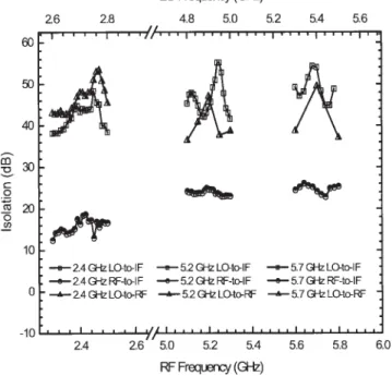
Figure 7 RF-to-IF isolation vs. RF frequency, LO-to-RF and LO-to-IF vs. LO frequency for the Gilbert downconverter with cascode current mirror RF input stage
Figure 8 Conversion gain vs. RF input power at 2.4, 5.2, and 5.7 GHz for the Gilbert downconverter with cascode current mirror RF input stage
3. EXPERIMENTAL RESULTS
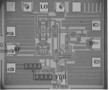
The chip was implemented in the 0.18-m CMOS technology. The photograph of chip is shown in Figure 3 and its size is 0.9⫻ 0.7 mm2. Measurements were performed by the on-wafer probing.
This mixer has single-ended RF and IF. The differential LO signals were generated from a commercial wideband 180° hybrid. A phase shifter is used to compensate the delay mismatch of two differen-tial paths. The measurements were performed at RF frequencies of 2.4, 5.2, and 5.7 GHz with a fixed IF of 300 MHz.
The RF input return losses at 2.4, 5.2, and 5.7 GHz are⫺14.6, ⫺9.4, and ⫺8.78 dB, respectively, as shown in Figure 4. The IF output return loss is 13.45 dB at 300 MHz.
Conversion gain vs. LO power when RF power is⫺40 dBm is shown in Figure 5. The chip generates the maximum gain with LO power of⫺4 dBm at 2.4 GHz, of ⫺3 dBm at 5.2 GHz, and of ⫺2 dBm at 5.7 GHz, respectively. The maximum gain is about 12 dB at 2.4 GHz and is 7.5 dB at 5.2 and 5.7 GHz. Because of the same IF frequency, the differences of gain at triple bands are attributed to the different transconductance of the RF input stage. Gain decreases with transconductance when frequency increases.
Figure 6 represents the conversion gain vs. RF frequency. These results were measured with a fixed IF of 300 MHz, while sweeping RF and LO frequencies at the same time.
The performance of port-to-port isolation is one of the impor-tant features in this design. High LO-to-IF isolation is expected because of the balanced DC output current of the improved cas-code current mirror RF input stage. The measurement results of port-to-port isolation at three bands are illustrated in Figure 7. For the isolation measurements, the IF frequency is fixed, and RF and LO frequencies are swept simultaneously. The RF-to-IF isolation is obtained by measuring the RF leakage power at the IF-port output. IF frequency is kept at 300 MHz for all the measure-ments. The fully integrated downconversion micromixer has LO-to-IF isolation of 43 dB, LO-to-RF isolation of 48 dB, and RF-to-IF isolation of 18 dB at 2.4 GHz. The micromixer has LO-to-IF isolation of 45 dB, LO-to-RF isolation of 47.5 dB, and RF-to-IF isolation of 25 dB at 5.2 GHz. The mixer also has LO-to-IF isolation of 54 dB, LO-to-RF isolation of 49.5 dB, and RF-to-IF isolation of 25 dB at 5.7 GHz. The LO-to-IF isolation is very good as expected. The total quiescent current of the circuit is about 7.6 mA at supply voltage of 1.8 V. The LO-to-IF isolation is much higher than the measured results in the paper [7]. To measure the input-referred 1 dB compression point (IP1dB), the chip was fed with the optimal fixed LO power and the RF power is swept from⫺40 to 0 dBm. As shown in Figure 8, IP1dB is⫺30 dBm at 2.4 GHz, ⫺25 dBm at 5.2 and 5.7 GHz. Notice that
the output-referred 1 dB compression points (OP1dB) are close at
three frequencies. The third-order intercept point (IP3) is also measured. OIP3 is⫺5 dBm at 2.4 GHz, ⫺6.5 dBm at 5.2 GHz, and⫺7 dBm at 5.7 GHz. The OIP3 and OP1dBof three bands are almost the same possibly because the gain compression is domi-nated by the IF output stage.
Double side band (DSB) noise was also measured for the mixer. The noise figure is about 24.5 dB at 5.2 GHz and 23 dB at 5.7 GHz. High noise figure results from too many transistors, and however, it can be diminished by the gain of LNA in all systems [9]. All of the measured results are summarized in Table 1. 4. CONCLUSION
A wideband micromixer with the low voltage cascode current mirror RF input stage is demonstrated in this paper. This mixer could work at three bands of Wireless LAN with low voltage supply. It has very high LO-to-IF port-to-port isolation because the low voltage cascode current mirror can have truly balanced DC currents. Higher isolation can be achieved at the cost of noise figure, but high noise figure can be reduced by the gain of LNA in all systems. The OIP3 and OP1dB
of three bands are almost the same possibly because the gain com-pression is dominated by the IF output stage.
ACKNOWLEDGMENT
This work was supported in part by the National Science Council of Republic of China under contract NSC 94 –2752-E-009 – 001-PAE, NSC 94 –2219-E-009 – 014, in part by the Ministry of Eco-nomic Affairs under contract 94-EC-17-A-05-S1– 020, and by the National Chip Implementation Center (CIC).
REFERENCES
1. B. Razavi, RF Microelectronics, Prentice Hall, Englewood Cliffs, NJ, 2001, chapter 6.
2. A.S. Sedra and K.C. Smith, Microelectronic circuits, 4th ed., Oxford University Press, Oxford, 1998. p. 640.
3. B. Gilbert, The Micromixer: A highly linear variant of the Gilbert mixer using a bisymmetric Class-AB input stage, IEEE J Solid-State Circuits 32 (1997), 1412–1423.
4. B. Razavi, Design of analog CMOS integrated circuits, McGraw-Hill, New York, 2001, chapter 5.
5. K.L. Fong and R.G. Meyer, Monolithic RF active mixer design, IEEE Trans Circuits Syst Part II 46 (1999), 231–239.
6. D. Johns and K. Martin, Analog integrated circuit design, Wiley, New York, 1997, chapter 6.
7. B. Razavi, Design of analog CMOS integrated circuits, McGraw-Hill, New York, 2001, chapter 9.
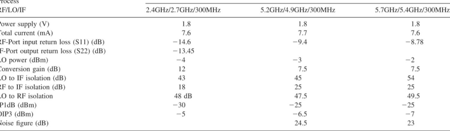
TABLE 1 Measured IC Performance
Process RF/LO/IF
TSMC 0.18um CMOS
2.4GHz/2.7GHz/300MHz 5.2GHz/4.9GHz/300MHz 5.7GHz/5.4GHz/300MHz
Power supply (V) 1.8 1.8 1.8
Total current (mA) 7.6 7.7 7.6
RF-Port input return loss (S11) (dB) ⫺14.6 ⫺9.4 ⫺8.78
IF-Port output return loss (S22) (dB) ⫺13.45
LO power (dBm) ⫺4 ⫺3 ⫺2 Conversion gain (dB) 12 7.5 7.5 LO to IF isolation (dB) 43 45 54 RF to IF isolation (dB) 18 25 25 LO to RF isolation 48 dB 47.5 49.5 IP1dB (dBm) ⫺30 ⫺25 ⫺25 OIP3 (dBm) ⫺5 ⫺6.5 ⫺7 Noise figure (dB) 24.5 23
8. C.C. Meng, S.K. Xu, T.H. Wu, M.H. Chao, and G.W. Huang, A high isolation CMFB downconversion micromixer using 0.18-m deep n-well CMOS technology, IEEE RFIC symposium, Philadelphia, PA June 2003. 9. K.-Y. Yeh, S.-S. Lu, and Y.-S. Lin, Monolithic InGaP-GaAs HBT receiver front-end with 6 mW DC power consumption for 5 GHz band WLAN applications, Electron Lett 40 (2004), 1542, 1543.
© 2006 Wiley Periodicals, Inc.
DUAL-BAND INTERNAL WLAN
ANTENNA FOR 2.4/5 GHz LAPTOP PC
APPLICATIONS
Young Jun Cho, Yong Sun Shin, and Seong-Ook Park School of Engineering
Information and Communications University Daejeon, Korea
Received 20 April 2006
ABSTRACT: This paper presents a dual-band internal WLAN PIFA for 2.4/5 GHz laptop applications in consideration of the influences of lap-top housing and LCD. The prototype antenna is modified when installed along the perimeter of the display panel of the laptop housing. The pro-posed antenna has a small ground plane and achieves an impedance bandwidth of 250 MHz (2.37–2.62 GHz) in Bluetooth band and 950 MHz (4.98 –5.93 GHz) near 5 GHz in WLAN band within 2:1 voltage standing wave ratio (VSWR). It also shows good antenna gain with small volume. These features make it an alternative for use in dual-band WLAN antennas. Design details for the proposed antenna in the case of the antenna itself, and the application of laptop PC housing are de-scribed, and experimental results of the antenna achievements are inves-tigated and discussed. © 2006 Wiley Periodicals, Inc. Microwave Opt Technol Lett 48: 2349 –2354, 2006; Published online in Wiley Inter-Science (www.interscience.wiley.com). DOI 10.1002/mop.21943 Key words: internal antennas; dual-band antennas; PIFA; laptop an-tennas; WLAN anan-tennas; installed inside a laptop
1. INTRODUCTION
Recently, as the service area of wireless local area networks (WLAN) communication is increasing, laptop computers are more and more being equipped with WLAN for the IEEE 802.11b (2.4 –2.48 GHz), 802.11a (5.15–5.35 GHz, 5.725–5.825 GHz) in the United States and HIPERLAN/2 (5.15–5.35 GHz, 5.47–5.725 GHz) protocols in Eu-rope [1, 2]. Herewith this dual-band pEu-roperty, one integrated single structure which requires a good performance, miniaturization, and moderate cost is an interesting trend in current research and is also in commercial demand. Multiple resonant paths in a single structure have been investigated because of the restraint on the physical size of internal antennas, and these not only improve aesthetic appearance, but also facilitate simple terminal design, compactness, serviceability, and robustness. Internal PIFAs are very suitable in WLAN applications, since they are compact, low profile, and easy to manufacture [3].
In this paper, a dual-band internal antenna of planar inverted-F antenna (PIFA) type is proposed for the dual band 802.11a/b and HIPERLAN/2, and built in actual laptop housing by modifying the initial prototype antenna and ground size. If the change tendency of the antenna performance for each associated case is investigated prior to the manufacturing of laptop applications, the antenna can be effectively remodeled in consideration of the performance ef-fects in a real situation, thus reducing trial and error. Both the radiation patch and small ground plate are made of the same copper plate with a thickness of 0.2 mm. It is directly fed by a 50
⍀ coaxial cable. It can be easily placed along the perimeter or at the corners of the display panel of the laptop computer. The proposed antenna is designed to resonate at frequencies of 2.4 and 5 GHz band by adjusting the location of the shorting pin and the length of the radiation element. The proposed antenna installed in commer-cial laptop PC housing can achieve the measured impedance band-width of 250 MHz at a lower frequency of 2.4 GHz band (2.37–2.62 GHz) and 950 MHz at a higher band of 5 GHz (4.98 –5.93 GHz). The radiation patterns are approximately omni-directional at each associ-ated frequency band in the case of the antenna itself. However, those patterns are influenced by the laptop housing when the modified antenna is installed inside it. The proposed antenna can provide a sufficient bandwidth for applications of IEEE 802.11a/b in the United States and HIPERLAN/2 in Europe, and offer high gains of 2.91 dBi at 2.44 GHz and 6.48 dBi at 5.8 GHz, respectively.
2. THE PROPOSED ANTENNA DESIGN, AND MEASURED AND SIMULATED RESULTS
2.1. The Prototype Antenna
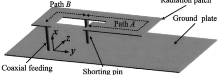
Figures 1 and 2 show the structure of the proposed dual-band prototype antenna with a PIFA type. It is composed of a radiation element with a hook shape and a rectangular ground plate of small size. The radiation element is physically supported by a coaxial cable and shorting pin. They electronically consist of a feeding structure. The 50⍀ coaxial cable directly feeds to a radiation patch by an inner conductor. The outer one is vertically connected to the small ground plate. The total size of the proposed antenna and ground has a volume of 47.5⫻ 20 ⫻ 7 mm3. For achieving the
resonant mode at 2.4 GHz band, the resonant length marked in Path A starting from the shorting point to the open end of the radiation patch is chosen to be about 32 mm corresponding ap-proximately to a quarter wavelength of 2.4 GHz, as shown in Figures 1 and 2(a). The length between the feeding and shorting point marked in Path B is about 12 mm in Figures 1 and 2(c). It is selected as an electrically quarter wavelength at the resonant frequency of 5.5 GHz band. To determine the dual resonant frequencies, Figure 3 shows the variations of VSWR values, according to the different position of the short pin and the length of the radiation element. Figure 3 (a) indicates each associated VSWR graph with three different values of with a fixed length of ⫽ 16 mm. The variations of length, aLand aRare 2 mm in the
opposite direction and the compared total lengths of are 10, 12, and 14 mm from reference line (ra) to the shorting point. As shown
in Figure 1, the variations of a shorting position make the length of Path A and Path B change, simultaneously. When the length of is shorter ( ⫽ 10 mm), the lower resonant band shifts to the left and the higher one to the right at the same time because the shorter the length of , the longer the one of Path A in regard to the Bluetooth band and the shorter the one of Path B in regard to the WLAN band, simultaneously. Similarly, Figure 3 (b) shows the variation of VSWR in terms of three different values of with the