行政院國家科學委員會專題研究計畫 成果報告
總計畫(3/3)
計畫類別: 整合型計畫 計畫編號: NSC91-2212-E-009-038- 執行期間: 91 年 08 月 01 日至 92 年 07 月 31 日 執行單位: 國立交通大學機械工程研究所 計畫主持人: 林清發 共同主持人: 曲新生,曾俊元 報告類型: 完整報告 處理方式: 本計畫可公開查詢中 華 民 國 92 年 11 月 4 日
行政院國家科學委員會補助專題研究計畫
□ 成 果 報 告
□期中進度報告
(計畫名稱)
12 吋矽晶圓半導體 CVD 製程設備及 BST 介電薄膜成長研究-總計畫(3/3)
計畫類別:□ 個別型計畫 □ 整合型計畫
計畫編號:NSC 91-2212-E-009-038-
執行期間:2002 年 08 月 01 日至 2003 年 07 月 31 日
計畫主持人:林清發
共同主持人:曲新生、曾俊元
計畫參與人員:
成果報告類型(依經費核定清單規定繳交):□精簡報告 □完整報告
本成果報告包括以下應繳交之附件:
□赴國外出差或研習心得報告一份
□赴大陸地區出差或研習心得報告一份
□出席國際學術會議心得報告及發表之論文各一份
□國際合作研究計畫國外研究報告書一份
處理方式:除產學合作研究計畫、提升產業技術及人才培育研究計畫、
列管計畫及下列情形者外,得立即公開查詢
□涉及專利或其他智慧財產權,□一年□二年後可公開查詢
執行單位:國立交通大學
中 華 民 國 九十二 年 七 月 三十一 日
√
√
√
ABSTRACT
This three-year group research project designs and establishes an experimental RTP (Rapid Thermal Processing) processor for a 12-inch single silicon wafer. There are three individual projects in this group research project. The first individual project designs and builds the heating and temperature control system for the 12-inch single wafer RTP processor and the integration of various components to form a RTP system. The major task in the second individual project is to measure the thermalphysical properties of the BST film and silicon wafer and analyze the thermal stress in the 12-inch silicon wafer. While in the third individual project the process parameters for the BST thin film growth are determined. Besides, the micro-structure of the BST thin film is analyzed and the material and electrical properties of the film are measured. The results from this individual project provide the data for the design of the processor in the first individual project.
These individual projects have integrated together through regular iterative discussion and interactive tests and improvement of the system design. The details on these results can be found in the complete reports for each individual project. Some major results from the three individual projects are summarized in this report.
摘要
本三年期整合型計畫主要為設計及建立快速加熱製程(RTP)設備以應用在 12 吋單一晶圓的製程上。此整合型計畫主要包含三個子計畫;子計畫一主要是 對12 吋晶圓建立一具有加熱及溫度控制單元及整合各種元件之快速加熱製程系 統。子計畫二的主要工作為量測鋇鍶鈦 (BST)薄膜之熱物理性質及分析晶圓所受 之熱應力。而子計畫三主要是決定影響鋇鍶鈦薄膜成長之製程參數。另外,本計 畫也分析鋇鍶鈦薄膜的微結構性質和量測薄膜的材料特性及電性。而子計畫三所 得到之結果將來可提供子計畫一設計RTP 爐之參考。 這些子計畫間之整合係透過一連串的討論及測試以提供系統設計之改進。 整合型計畫獲得的詳細結果可由各子計畫整合之精簡報告而得知。同時在這份報 告我們將列出各子計畫之主要結果。 關鍵字:RTP 爐體設計、BST 薄膜成長Content
Abstract···I 摘要···II Content···III List of Figures···IV Chapter 1 Introduction···1Chapter 2 Experimental Apparatus···11
2.1 Processing Chamber···11
2.2 Temperature Measurement and Data Acquisition Unit···11
2.3 Heating Unit (Lamp & Resistance Heating)···12
2.4 Gas Injection Unit···12
2.5 Vacuum Unit···13
2.6 Control Unit···13
Chapter 3 Results and Discussion···14
3.1 The temperature uniformity of wafer···14
3.2 Temperature Uniformity of Silicon Wafers during RTP and Spectral Properties of BST thin films···15
3.2.1 Spectral Properties of BST thin films···17
3.3 BST thin films and their electrical properties···17
3.3.1 Phase formation characteristics···19
3.3.2 Leakage current characteristics···20
3.3.3 Effect of concentration on the J-E characteristics···22
3.3.4 Dielectric properties···23
Chapter 4 Concluding Remarks···26
List of Table and Figures
Table 3.1 Lattice parameter after annealing the thin film at different temperatures calculated using (1 1 0) reflection and Pt (1 1 1) peak as the standard.
Fig. 3.1 Photo of four-zone heating lamp assembly.
Fig. 3.2 Photo of six-zone resistance heater.
Fig. 3.3 The temperature distribution on the wafer at selected locations for
Tset=250℃ & Q=1slpm with the lamp & resistance heating.
Fig. 3.4 Schematic representation of energy flux in a wafer under incident heat
flux and radiant heat losses emitted from all surfaces.
Fig. 3.5 Inverse incident-heat-flux profiles results for a measurement error of
σ=0.0 at linear ramp-up rates of (a) 100oC/sec (b) 200oC/sec, and (c)
300oC/sec.
Fig. 3.6 Inverse incident-heat-flux thermal non-uniformity profile results for a
measurement error of σ =0.0 at linear ramp-up rates of (a) 100oC/sec,
(b) 200oC/sec and (c) 300 oC/sec.
Fig. 3.7 Resulting maximum temperature difference for measurement errors of
σ
=0.0,σ
=0.001,σ
=0.003 andσ
=0.005 as a function of the linearramp-up rate.
Fig. 3.8 Variation of transmittance as a function of wavelength for different
thickness of the BST thin films.
Fig. 3.9 Variation of reflectance as a function of wavelength for different
thickness of the BST thin films.
Fig. 3.10 The refractive index of the BST thin films for different thickness. Fig. 3.11 The absorption index of the BST thin films for different thickness.
Fig. 3.12 Variation of reflectance as a function of wavelength for different temperature of the BST thin films.
Fig. 3.13 Variation of the thickness of the 500 ℃pyrolysed film after annealing at different temperatures determined using SEM cross-sectional image. Fig. 3.14 SEM (a) surface and (b) cross-sectional image of Pt/Ti/SiO2/Si wafer
after annealing at 800℃ for 2 h showing the TiOx islands on the surface of Pt film formed by the migration of Ti through the Pt-grain boundaries. The thickness of the interfacial layer formed is about 128
nm.
Fig. 3.15 J–E plot of BST thin films post-annealed at different temperatures for 2 h in air.
Fig. 3.16 Verification of the second order power dependence of the leakage
current density at 100 kV/cm (J100 kV/cm) against the Ag content in the
BST films according to percolation theory for a metal-dielectric composite.
Fig. 3.17 J–E plot of BST thin films prepared from precursor solutions ofthree different concentrations and post-annealed at 700℃ per 2 h in air. Fig. 3.18 (a) Variation of the 100 kHz dielectric constant with applied electric
field for the BST thin films annealed at different temperatures for 2 h in air and (b) Variationof the loss tangent with applied electric field for the BST thin films annealed at different temperatures for 2 h in air.
Fig. 3.19 Capacitance vs. Voltage characteristics for Ag (0, 1, 2, 3, 4, 6)-BST thin films.
Fig. 3.20 Comparison of dielectric loss measured for 2 % Ag-doped BST (Ag(2)-BST) film with the loss characteristics recorded for 0, 1, 3 and 4 %-Ag-doped BST films.
CHAPTER 1
INTRODUCTION
The relevant literature on the chemical vapor deposition of thin films is reviwed first. Özturk et al.[1] proposed that three challenging issues needed to be addressed in the design of a lamp heated rapid thermal reactor for growing a thin solid film: (1) for getting a uniform thin film, the thickness of the velocity, temperature, and concentration boundary layers must be uniform so that the deposition rate on the wafer will be uniform; (2) to reduce the thermal stresses and temperature gradient on wafer; (3) for interface abruptness, the gas flow in the reactor must be free of any laminar vortices to minimize gas residence time.
Depending on the flow and thermal conditions there are two fundamental types of flow regimes in a vertical MOCVD (Metal-Organic Chemical Vapor Deposition) reactor [2]: (1) plug flow, where the gas flows smoothly over the substrate without any circulation in the reactor and (2) buoyancy-induced flow, where the buoyancy force associated with the temperature gradient in the gas flow will induce upward flow recirculation. It has been found that rotation of the wafer can be used to establish a self-similar velocity profile along the substrate [2&3], which produces a uniform boundary layer [4] and can also stabilize the flow. The effects of the gas injection and mass flow rate, disk rotation and heating, and reactor pressure on the flow pattern were studied by Wang [3]. The effect of the reactor geometry has been studied by Gadgil [5]. He indicated that a reactor with a gradually expanding cross section could sustain a smooth and streamline flow at a high temperature (773K) without the need for external flow stabilizers. Such a reactor configuration could simplify the reactor design. The constraints of a stagnation point flow CVD (Chemical Vapor Deposition) reactor design are proposed by Gadgil [6]. His research showed that a gas distributor
such as a capillary plug in a stagnation point flow CVD reactor was highly essential to attain a highly uniform axially velocity profile. It is also shown that the smaller gas viscosity of inert gases such as argon or nitrogen is required to reduce the pressure drop across the gas distributor which will, in turn, lower the hydrodynamic boundary layer width on the substrate and thus form a more uniform deposition thickness.
A finite element solution based on three-dimensional models of transport phenomena in vertical MOCVD reactors was proposed to investigate the effects of operating conditions and heat transfer characteristics on the flow pattern and growth uniformity by Fotiads and Kieda [7]. They noted that as the gas entered the reactor through a single inlet tube, the recirculation cell could be eliminated by increasing the inlet gas flow rate and thus improved film uniformity considerably. In addition, reducing the total gas pressure in the reactor decreased the strength of the recirculation and eventually eliminated it. A similar conclusion was reached by Kleijn et al. [8] in numerically computing the gas flow for low pressure CVD in a single wafer reactor. They found that at a high total pressure (3-10 torrs) the buoyancy-induced recirulation cell may be induced when nitrogen is used as a carried
gas. Evans and Grief [9] also reported that for Re3/2/Gr<40 the flow is significant
influenced by the natural convection effect in a rotating disk reactor. Fotiads and Kieda[7] also indicated that shortening the distance between the gas inlet and susceptor will eliminate the convection cell because of the decrease of the buoyancy force and thus the inertia force dominated in the flow. Moreover, at a high inlet flow rate the decrease in the inlet diameter could eliminate the cell and the uniformity was improved.
Rapid Thermal Processing (RTP) with its inherently smaller thermal mass has become a core technology step in manufacturing ULSI devices such as memory chips, microprocessors and logics. In many practical applications, RTP has been proven to
be a key technology in single wafer processing due to the smaller thermal budget and higher throughput [10, 11]. Moreover, RTP has the advantage of short ramp up and down periods. But, poor RTP system design can lead to significant temperature difference across the entire wafer and thus cause stress in the wafer. Above the plastic deformation limit this stress can not be relieved by the plastic deformation, which leads to the crystallographic slip [12 & 13] and disruption of circuit. The temperature uniformity of a wafer is of more and more concern with the increase in the wafer size simply because of the accompanying great wafer temperature gradient in the transient and steady state in a RTP system. Three principal effects were identified that lead to the temperature non-uniformity of a wafer during a rapid thermal process: edge effect, pattern effect and non-uniform source intensity.
In lamp heated, rapid thermal processors the higher radiative loss from the wafer edge was found to result in a radial temperature gradient in the wafer [12&13]. This temperature gradient induces a thermal stress which is compressive in central region of the wafer but is tensile toward the edge of the wafer by Sorrell et al. [14]. They simulated the heat transfer to a wafer in a RTP reactor by an analytical/numerical model and used the geometric optics to predict the radiant heat flux distribution over the wafer at a pressure of 0.5 - 5 torrs and for the wafer temperature above 600 ℃. Results from their model indicated that it was difficult to produce the desired irradiance distribution in a RTP by employing only the flat reflector. Focusing reflectors can be used to give a heat flux distribution that substantially improved the temperature uniformity. They also proposed the method to achieve uniform heat flux and possibly uniform wafer temperature by arranging the heating lamps into concentric heating zones and operated with the outer lamps at a higher power. In a numerical study, Campbell et al. [15] gave a two-dimensional solution to the recirculating flow in a RTP reactor including the convective gas flow
effect. Their results showed that the gas flow had a negligible effect in a low-pressure CVD reactor.
In examining the dynamics of the gas flow in a rapid thermal processor during the heating step, Nenyei et al.[16] found that a multiple gas baffle system, dynamic gas handling , low pressure operation, low temperature edge guard ring and independent top and bottom heater bank control were the proper tools for optimizing the gas flow in the processor. To improve the wafer temperature non-uniformity produced by the edge effect, a cone-shape shield was placed at the edge of the wafer to reduce the heat loss from the wafer edge and to reflect the radiative energy back into the wafer [17&18]. By varying the angle of the conic section, an optimal shield configuration can be found to minimize the induced thermal stress. Cho and Kin [19] proposed to use a ring of silicon dioxide formed at the wafer edge to reduce the heat lose by the wafer edge. A three-dimension model was proposed by Zllner et al. [20] to investigate the influence of the wafer edge without taking the convective heat transfer into account. Their result showed that the peripheral temperature drop could be compensated by a separate focusing lamp ring. Another way to reduce the edge effect is to provide a supplementary heat source surrounding the wafer [21&22]. A passive guard ring such as an independent heated ring [23] or an annual lamp [24] was noted to improve the wafer temperature uniformity. Moreover, the guard rings can reduce the temperature-gradient-induced wafer deformation by a factor of ten when compared to a freestanding wafer [25]. A simple method for solving the temperature non-uniformity in a RTP system was proposed by Kuo et al. [26]. They use concentric Si rings on a planar quartz or Si susceptor to improve the wafer temperature distribution. It was noted that although the use of a guard ring can improve the wafer temperature uniformity, significant temperature gradient can exist in the ring causing it to become warped.
Another type of the wafer temperature non-uniformity results from the local differences in the radiation absorption and emissivity of the wafer surface induced by the pattern on the wafer [27]. Vandenabeele et al. [28] experimentally and theoretically showed that the patterned oxide layers could cause steady state and transient wafer temperature non-uniformity up to 80 K. Jeffery et al. [29] have showed that the patterns can have some extreme effects on the transient and steady state temperature uniformity in a single-side illumination RTP system. They further suggested that the temperature non-uniformity in any patterned wafer arose from the different radiative properties on the back, front and edge of the wafer. These radiation properties, in turn, are affected by the pattern, film thickness and surface roughness. Further research showed that the patterns on the wafer could affect radiative properties [28], heating rates [27 & 28], temperature uniformity [27 & 28], wafer wrapage [30] and localized stress in the wafer [31]. Wong and Miaoulis et al [4, 32] numerically investigated the effect of patterning in wafers on the absorption characteristics, temperature uniformity and processing uniformity during RTP. Their results indicated that the processing uniformity was affected by the patterns themselves as well as by the heating characteristics of the wafer. A direct mean to avoid the effects of the patterns on the wafers is to heat the wafers at backside of the wafer. Vandenabeele et al. [28] suggested that the problem of different absorption on patterned wafer could be best solved by using backside illumination. To solve the problem associated with the different emissivity, a remote and highly reflective reflector is recommended. One way to obtain uniform radiation or re-radiation to the wafer is to redistribute the energy by properly shaping both the heat source and the processing chamber. This can be realized by using a light pipe which collects the energy from the light source and reflect many times, then re-distributes the energy over the cross-sectional area of the light pipe. For a square light pipe of a cross
sectional area R2 with length L and wall reflectivity being unity, Chen et al. [33] showed that the flux density at the exit plane converged to unity as the aspect ratio L/R →∞. This signifies that the higher are the light pipe’s aspect ratio and reflectivity, the light ray experiences more reflection before reaching the exit and more uniform flux distribution is obtained. The concept of multiple reflections by the light pipes with the high reflectivity and high aspect ratio relating to the reflective cavity was investigated by Sheets [34&35]. They concluded that a reactor chamber with high aspect ratio and high reflectivity wall led to an increasing effective emissivity and thus to a better uniformity. But the increase in the aspect ratio of the reactor requires more lamp power to compensate the energy loss at the wall. One disadvantage of such highly reflective chamber is that at a high aspect ratio the wall needs to be cooled down during the lamp off period.
Other means to improve the temperature uniformity of the wafer are through the control and arrangement of the lamps. It is easy to realize that the non-uniform heat flux intensity from the lamps will lead to severe temperature non-uniformity in the wafer during the rapid thermal processing. In order to get fast ramp-up and ramp-down processes, a quick response sensing means for the wafer temperature measurement and a computer program which can continuously monitor the wafer temperature and control the power of the heat source are required [36]. Thermal processes in RTP are known to be highly nonlinear and distributed in nature. In-situ sensors can be used to measure the major state parameters including wafer temperature, sheet resistance, layer thickness, stress and surface roughness. These sensors may provide single-point or multi-point measurements. A multi-zone controller was implemented to improve the RTP repeatability and uniformity [37]. Uniform wafer heating was achieved by employing the multi-point pyrometer signals along with a multivariable controller. An Internal Model Control (IMC) law design
methodology was suggested by Schaper et al. [38] to automatically compute the lamp power to an array of concentric heating zones to achieve wafer temperature uniformity. On the other hand, Gyursik et al. [39] proposed an equipment model method to determine the relative power setting of the reactor lamps needed to optimize the temperature uniformity in the wafer.
In the lamp arrangement, Moslehi et al. [10&40] and Spence et al. [41] showed that an axi-symmetrical RTP equipment design provided a better conformance to the circular shape of silicon wafers compared to the conventional linear lamp array RTP system. In general, an axi-symmetrical RTP with a dynamic multi-zone temperature control provides the best overall tool performance.
Pushkar et al. [42] proposed a three-zone lamp system in which the tungsten-halogen lamps are configured in three concentric rings that are independently and dynamically controlled. The arrangement offers a significant improved temperature uniformity.
An important problem in RTP temperature is to obtain accurate temperature measurement. Two basic sensors are normally used to measure the wafer temperature in rapid thermal processing, namely, thermocouple and pyrometer. The generally accepted method for measuring the wafer temperature is by means of a properly embedded and corrected thermocouple [43]. The thermocouple bead must be in intimate thermal contact with the interior of the wafer over as large as the bead as possible and the whole surface area of the bead must absorb and reflect radiation in a similar way to the wafer itself. The use of the thermocouple has advantages of being simple, low cost and easy. But it’s not practicable to embed thermocouples into every wafer to be processed. A pyrometer, however, becomes most widely used for the temperature measurement in RTP systems. Basically, a pyrometer determines the wafer temperature indirectly by measuring the thermal radiation emitted from a
particular point in the wafer. Since the wafer’s emissivity changes during a process, the temperature estimation based on the radiation reading is not easy and requires a model-based fitting algorithm. Moreover, the pyrometric measurements are degraded by the additional influences from the lamps. Real-time compensation for changing emissivity of the wafer and the lamp influences requires an accurate modeling, model parameter identification and real-time filtering. Belikov [44] used a dynamic observer to identify the lamp radiation function and used it to control a five-zone RTP reactor. They proposed to compensate the influences resulting from the uncertainty of wafer emissivity, lamp interference and window/chamber heating effect by using a real-time computational algorithm based on a physical model for the pyrometeric detectors and wafer temperature dynamics. Xu and Sturm [45] investigated the effects of the front-side reflective surfaces on the emissivity and temperature measurement of silicon wafers in a RTP chamber with the backside heating through optical modeling. They concluded that the measured temperature error produced by the emissivity error is very sensitive to the reflector quality.
Another indirect measurement technique, the so called “ripple technique”, was recently developed to deal with the trouble associated with the unknown wafer emissivity and unknown background in using a pyrometer [46]. The ripple technique takes advantage of the peak lamp emission instead of avoiding it. This method used two optical fibers made of quartz or sapphire with wide numerical apertures. Two fiber sensors are used, one collects the lamplight and the other collects the emission from the hot wafer and the reflected background lamplight. The ripple technique successfully subtracts the background light and calculates the wafer temperature.
After approximately 50,000 wafers were processed for annealing at 900 to 1000
℃
pyrometer in their test procedures was within 6 ℃ at one standard deviation. Moreover, a real-time acoustic thermometer has been used to measure the wafer temperature during the rapid thermal processing, which allowed us to obtain a complete wafer temperature tomography under all process condition [48]. The backside roughness of the wafer does not affect the acoustic wave, since it is very small as compared to the wavelength which is in the order of centimeter. They claimed that it was possible to measure the wafer temperature in-situ in 0-1000℃ range with 1℃ accuracy. Moreover, a sub-feature speckle interferometry was also applied to the task of temperature measurement by Burckel et al. [49], which offers improved measured speed and much higher resolution than traditional full-field speckle intensity correlation technologies. In their research, they demonstrated a measurement precision of 0.92 ℃ for a radiatively heated Si wafer up to 220 ℃.
In view of the continuing miniaturization of the IC components and increasing functions and performance of a single IC chip in recent and coming years, integration of the IC components in a large wafer is needed and the integration has moved from VLSI to ULSI. Successful fabrication of the extremely dense submicron circuits on a 12-inch wafer are facing the problem of temperature nonuniformity on the wafer which has low thermal conductivity and bad gas flow distribution in the vicinity of the wafer so the concentration of the precursor gases and chemical reactions are nonuniform on the wafer. In this three-year research project, we design and establish an experimental CVD (Chemical Vapor Deposition) reactor for a 12-inch single silicon wafer. In the present study the heating unit for the 12” wafer redesigned for the purpose improving the wafer temperature uniformity. Besides, the reactor is especially designed for the growth of the BST thin film. This film is considered to be a very suitable dielectric layer for the future DRAM with capacity larger than 1 Gbit. In addition, this project investigates the process parameters for the BST thin film growth
on the silicon wafer, the micro-structure of the BST thin film and measured the thermalphysical, material and electrical properties of the film.
There are three individual projects in this group research project. The first individual project designs and builds the heating and temperature control system for the 12-inch single wafer CVD reactor to improve the temperature uniformity. Various components are integrated to form a RTCVD reactor system. The major task in the second individual project is to measure the reflectivity and transmittivity of the BST film and 12-inch silicon wafer. It is interesting to note that reflectivity and transmittivity have significant effects on the temperature uniformity especially for a large wafer. However, in this individual project, we also want to develop the thermal radiation model for the RTP processor and assess the shape of the reactor chamber, heating methods, guard ring and heating lamp arrangement. While in the third individual project the process parameters for the BST thin film growth are determined. Besides, the micro-structure of the BST thin film is analyzed and the material and electrical properties of the film are measured. The results from this study will provide the data for the design of the reactor in the first individual project.
CHAPTER 2
EXPERIMENTAL APPARATUS
A model RTP processor for a 12-inch single silicon wafer is established in this project. The system is an experimental lamp heated, rapid thermal processor designed mainly to study the wafer temperature uniformity during the ramp-up stage. The system consists of six major parts: (1) processing chamber, (2) temperature measurement and data acquisition unit, (3) heating lamp unit, (4) gas injection unit, (5) vacuum unit, and (6) control unit. They are described briefly in the following.
2.1 Processing Chamber
The processing chamber of the present experimental RTP processor is cylindrical and has a diameter of 40.8 cm. Its sidewall is made of stainless steel coated with thin gold film to increase its reflection of light from the lamps. In the present experiment we use a 12-in silicon circular wafer so that a somewhat non-isothermal boundary condition on the wafer surface is obtained even with a complicate control of the multi-zone heating lamp unit. There are Eight T-type thermocouples stuck on the wafer at selected locations to measure the temperature variations over the wafer. It should be mentioned that there are two susceptors (quartz and copper) tested in this study.
2.2 Temperature Measurement and Data Acquisition Unit
As mentioned above, the distribution of the wafer surface temperature and the feedback control signals are measured by thirteen K-type thermocouples at selected detection locations on the surface of the wafer. The temperature measurement system consists of the wafer temperature measured from TC Wafer and recorded by PDA (manufactured by SensArry Corp.) and the control system feedback with four K-type thermocouples for the lamp heating system. The PDA recorded signals from the
measured temperature of the wafer surface combined with an industrial personal computer (IPC, ADVENTECH 600 series) and the four feedback temperature signals are transmitted to various transducers. The voltage signals from the four feedback thermocouples are converted to temperature using the ADVENTECH PCLD 789D A/D card by the internal calibration equation in the computer and are displayed on the screen simultaneously. These detected temperatures are also feedbacked to adjust the input power to the lamps intending to improve the uniformity of wafer temperature.
2.3 Heating Lamp Unit
The lamp-heating unit consists of twenty-nine lamps and cooling fans. The lamps provide the thermal radiative energy to the wafer through a quartz window. More specifically, the twenty-nine 1000W & 82V OSRAM tungsten-halogen lamps (with reflector) are arranged into four zones: the first zone has one lamp, the second and third zones each have eight lamps, and the outer zone has twelve lamps (Figs. 2.4 & 2.7 (a)). The power input to each lamp zone can be automatically adjusted according to the feedback control signals in real time using four SCR power regulators for optimal wafer temperature uniformity. Besides, for further improving the temperature uniformity of the wafer we also introduce a resistance heater which consists of a high thermal conductivity copper plate and heater coil under the wafer. This heater has six heating zones so that we can independently control the power of each heating zone.
2.4 Gas Injection Unit
The precursors of BST thin film, like Ba or Sr, are all solid at room temperature so we input these precursors into the a pressurized bath (THF) and change them to liquid sources. These sources have a lower volatility and are easily decomposed at high temperature. For this purpose, we use the flash vaporization to vaporize these
through the mass flow controller (BROOK 5850E) to control the inlet mass flow rate. Then the gas flow from the connection pipes is injected into the mixing chamber through the nozzles installed on the sidewalls of the mixing chamber. The gas flows from the nozzles mix in the mixing chamber and then move through the showerhead into the processing chamber.
2.5 Vacuum Unit
To pump out the processed gas and to keep the processing chamber at the preset
pressure, a rotary vacuum pump (ALCATEL 2063C1) with a 60 m3/hr pumping
capacity is installed in the system. The pumping rate can be adjusted by a MKS 253B throttle valve and the gas leaving the processing chamber is sucked out to an exhaust gas treating unit. However, we also add a vacuum chamber to reduce the influence of the pulses produced by the vacuum pump. The system pressure of the chamber is maintained at the required level by adjusting the flow rate of the vacuum pump. Moreover, we also install a pressure controller (MKS 600 series) to control the chamber pressure.
2.6 Control Unit
To control the input power to the lamps, a fuzzy control algorithm is used to control the lamp power. A typical measured wafer temperature for the detection points at the geometrical center of the wafer controlled by the fuzzy control algorithm is rather stable at steady state in this RTP processor.
CHAPTER 3
RESULTS AND DISCUSSION
The major results obtained in each individual project are presented and discussed in this chapter. Complete results for each individual projects are available from the reports for each project.
3.1 The temperature uniformity of wafer
In the RTP processor, the temperature uniformity of wafer is an important factor for growing a uniform thin film. In the first individual project, we focus on the design of a new wafer heating and temperature control system to improve the temperature uniformity of the wafer. However, the temperature uniformity of wafer depends on the arrangement of lamps, the power control scheme of the lamps, the temperature detector, the geometry of the chamber, the types of susceptor and etc. To achieve this goal, we introduce a multi-zone lamp heating assembly with automatic lamp power control for each zone and an active six-zone resistance heater with isothermal circular copper plate placed just under the wafer to increase the temperature uniformity across the wafer.
As just mentioned, the temperature uniformity of the wafer depends largely on the heat flux from heating source to the wafer. For this purpose, we use the four-zone lamp heating with a fuzzy control model to adjust the input power actively. The photo of the multi zone lamp heating unit is shown in Fig. 3.1. It is important to note that the resistance heating can result in better wafer temperature uniformity than the lamp heating. So we introduce a six-zone resistance heater directly adhering to a 10-mm thick circular copper plate to improve the temperature uniformity, as shown in Fig. 3.2. However, only using the resistance heater will increase the processing time and power
consumption obviously. To avoid this disadvantage, it is of interest to investigate whether the installation of the six-zone active resistance heater along with the four-zone lamp heating can improve the uniformity of the wafer temperature and in the meantime reduce the processing time during the whole process. Moreover, the results from this study indicate that combining the four-zone lamp heating and six-zone active resistance heating does reduce the processing time and improve the temperature uniformity of the wafer. The gas is sent into the processor at the fixed temperature of 25℃. Note that at the input gas flow Q=1 slpm the temperature variation on the wafer is still small, as shown in Fig. 3.3.
3.2 Temperature Uniformity of Silicon Wafers during RTP and Spectral Properties of BST thin films
Since the wafer is so thin that the thermal non-uniformity may be insignificant in axial ( z ) direction, we concentrate on the wafer surface thermal non-uniformity in
radial (r) direction. Random measurement errors σ were added to the desired
temperature trajectories in simulation as described in the report for the second individual project. In the present study, the respective dimensional measured
temperatures n
T1,1± 0.7728
oC and n
T1,1± 3.864
oC were simulated for the cases of
σ
=0.001 andσ
=0.005 (Fig. 3.4).Figures 3.5(a)-(c) show the three-dimensional graph of the incident-heat-flux profiles calculated by inverse method on the wafer surface at a measurement error
σ
=0.0 for uniform temperature tracking of the 100, 200 and 300oC/sec ramp-up rates,respectively. Ramping of wafer temperature took place when there was an excess of absorbed energy over heat-loss energy. During the initial transient phase, the wafer temperature increased with the increasing energy absorption, and heat losses also
increased as the wafer temperature increased. The initial absorbed energy, required for wafer uniform-temperature tracking, was larger than that during other periods.
Inverse dynamic incident-heat-flux profile results for wafer surface thermal
non-uniformities at three linear ramp-up rates with a measurement error of σ =0.0
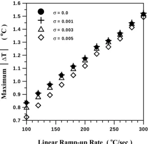
are shown in Figs. 3.6(a)-(c), respectively. These figures show that when incident heat-flux profiles are controlled as in our inverse-method approach, temperature differences develop at the edges of the wafers. Initially, the temperature difference (thermal non-uniformity) is not significant, however, as the ramp-up of the wafer proceeds, the thermal non-uniformity developed at the edge increases with increasing edge-heating compensation, as shown in Fig. 3.9. When the wafer reaches the higher steady state, the incident-heat-flux profile changes from the transient stage to the steady stage, the thermal non-uniformity drops gradually and approaches the steady-state. Thus, edge-heating compensation has an overheating effect on thermal uniformity during processing. The thermal non-uniformity was not significant in the present inverse incident-heat-flux profiles, even though during transient periods, resulting maximum temperature differences were 0835, 1.174 and 1.516℃ for the 100, 200 and 300 ℃/sec ramp-up rates, respectively. Figure 3.7 illustrates the
resulting maximum temperature differences (∆T , the absolute value of temperature
difference between the edge and the center of the wafer surface) during transients as a
function of the desired linear ramp-up rates for measurement errors of
σ
=0.0, 0.001,0.003 and 0.005, respectively. Our results show that the maximum temperature differences occurring during the ramp-up increased with the ramp-up rate. The thermal non-uniformity of the inverse results decreases with increasing measurement
error
σ
from 0.001 to 0.005. Although a linear ramp-up rate of 300oC/sec was usedtemperature was maintained within 1.6oC of the center of the wafer surface when the incident-heat-flux profiles were dynamically controlled according to the inverse-method approach. These thermal non-uniformities could be acceptable in RTP systems.
3.2.1 Spectral Properties of BST thin films
The transmittance and reflectance of BST thin films for various film thicknesses are in the near-mid infrared wavelength region, as shown Figs. 3.8 and 3.9. With increasing of the film thickness, the transmittance is increased and the vibration of reflectance is clearly observed. Figures 3.10 and 3.11 show that the refractive index and absorption index of BST thin films for various film thickness are in visible light
wavelength region. As the BST thin films thickness is 0.4µm, the highest refractive
index and absorptive index can be obtained. The value of absorptive index of BST thin films is close to zero at near-mid infrared region, but the maximum value of the refractive index appears at the visible light region. Hence, in view of the RTP process on BST thin films, the BST thin films thickness of 0.4µm is the best choice.
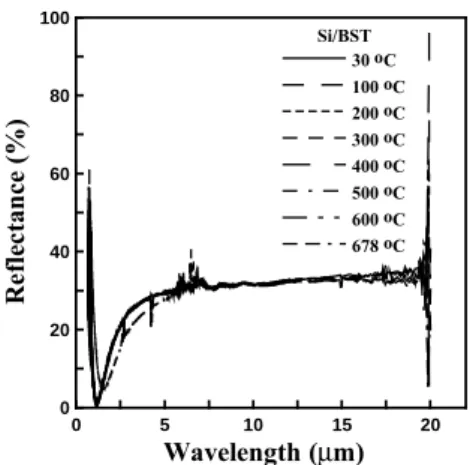
Figure 3.12 indicates that the reflectance of BST thin films for various heating temperatures in the near-mid infrared wavelength region. Results show that there is no manifest difference for reflectance analysis and has the tendency of shifting toward to
the short-wavelength in the temperatures ranging from 30 to 600 . For BST thin ℃ ℃
films, the reflectance tends to shift toward to the long-wavelength because thin film
structures have been transferred upon the temperature of 600 .℃
3.3 BST thin films and their electrical properties
In this section the results from the third individual project are summarized. The stabilisation of the precursor solution was a difficult step during the preparation of
BST films because of the molecular water associated with Ba- and Sr-hydroxides released to the solvent during the refluxing step resulted in preferential precipitation of the Ti by rigorous hydrolysis. This problem was overcome by individually reacting the starting materials with 2-methoxy ethanol and evaporating the water content in the Ba- and Sr-solution by refluxing for 3–4 h before mixing to form BST complex sol. The solution once stabilised can be stored for months without any precipitation. The individual precursor solution obtained by reacting the Ba-, Sr-hydroxides and Ti-isopropoxide with 2-methoxy ethanol were filtered and analysed by static gravimetry (by solvent evaporation of a small quantity of the solution and decomposing the resultant precursor at 700℃) prior to mixing them together to confirm the composition of the solution.
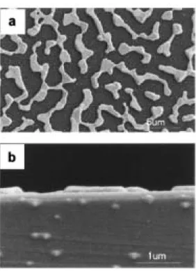
The BST film deposited on the Si/SiO2/Pt substrate peeled off very often on pyrolysis at the interface between bottom Pt-electrode and the Si/SiO2 substrate. This is mainly due to the poor adhesion of Pt-thin film on the Si/SiO2 substrate. The adhesion of bottom Pt-electrode on the Si/SiO2 substrate was greatly improved by depositing a 100 nm Ti buffer layer between Si/SiO2 and Pt layer. However, Ti buffer layer incorporation lead to added complexities by way of Ti-migration onto the surface of bottom Pt-electrode on annealing. Fig. 3.13 shows the thickness variation of the 500℃ pyrolysed thin film as a function of annealing temperature determined from the SEM cross-sectional image. The thickness of the sample increased initially up to an annealing temperature of 700℃ and thereafter showed a decrease. Fig. 3.14 shows the surface and cross-sectional image of 800℃ per2h annealed Pt/Ti/SiO2/Si wafer. Surface image shows the formation of random islands on the Pt surface due to the Ti-migration. The cross-sectional image shows that the thickness of each island is around 128 nm, which contributes to BST film thickness. The composition of this
surface discontinuous layer has been determined using XPS.
3.3.1 Phase formation characteristics
X-ray diffraction study of the films post-annealed at different temperatures indicated that reasonably well-crystallised films were obtained at a temperature as low as 500℃. The XRD pattern showed all major X-ray reflection peaks of perovskite BST phase indicating the polycrystalline nature of the film with (110) as the major peak. Crystallinity of the thin films improved with increase in the annealing temperature, indicated by the increase in intensity of the X-ray diffraction peaks. The average grain size was calculated by using the full width at half maximum of the dominant (110) peak using Scherrer’s equation. The 500℃annealed sample showed an average grain size of 20 nm, which increased to 32 nm on annealing above 600 ℃.
The grain size of the films increased with increasing annealing temperature. Increase in grain size with increasing annealing temperature is expected because of the sintering wherein the small grains coalesce to form larger grains. Lattice parameter of the thin films annealed in the temperature range 500 – 700℃ remained almost constant (Table 3.1). However, when annealed at temperatures above 700℃, a small decrease is observed. Film annealed at 800℃ showed 0.02Å contraction in lattice parameter with respect to the film annealed at 500℃. This type of lattice shrinkage was also observed in sputtered BaTiO3 and BST, which has been attributed to non-equilibrium and highly distorted states within the films. This indicates that the low-temperature annealed films are in more strained form and the atomic entities must have been in the non-equilibrium positions which relax to the equilibrium position when annealed at higher temperatures, hence a contraction in lattice parameter is
obvious. Similarly, XRD patterns were obtained for the films prepared from different concentration solutions (0.08, 0.15 and 0.28 M) on to platinised Si-wafer, which showed phase pure BST thin films. The average grain size calculated using Scherrer’s equation was approximately 32 nm.
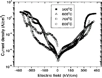
3.3.2 Leakage current characteristics
The leakage current density vs. electric field (J–E) plot of the BST thin films annealed at different temperatures is shown in Fig. 3.15, which shows variation with annealing temperature. In the positive voltage region of J–E plot, film annealed at 500 ℃ shows larger leakage current than that annealed at higher temperatures. Lowest leakage current is observed for the film annealed at 600 and 700℃. The 800℃ annealed film shows slightly higher leakage current than 600 and 700℃ annealed films but is lower than 500℃ annealed film. The J–E characteristics of all the samples show three different regions indicating the contribution from three different types of conduction mechanisms at low, intermediate and high field regions. At lower voltage the film shows ohmic behaviour (J α E) and deviates at intermediate and higher fields. The turn-on electric field from ohmic to non-ohmic region decreased as the annealing temperature increased. The turn-on electric field for the sample
annealed at 500 and 600℃ is around 300 kV cm–1 and that of film annealed at 700
and 800℃ is around 200 and 150 kV cm–1, respectively. The leakage current
characteristics of the thin film capacitor depends upon several factors such as the top and bottom electrode interface, surface roughness, the integrity of the electrodes, formation of interfacial low impedance layer or presence of any impurity second phase in the dielectric film which provides an easy path for electrons which can dramatically increase the leakage current. Formation of hillocks on the bottom
Pt-electrode due to repeated thermal cycling is another reason for the increased leakage current in sol–gel derived films. High leakage current observed in the case of 500℃ annealed samples might be due to the presence of embedded pyrolysed decomposition products in the film.
The decrease in the leakage current with increase in annealing temperature is because of the burn-off of these embedded decomposition products. Increase in leakage current for the film annealed at 800 ℃is due to the increase in the grain size, as observed by SEM analysis, which contributes to surface roughness. The grain size of the film could play an important role in deciding the surface roughness; the small grain size films usually have smooth surface and low leakage current. SEM surface analysis of the 500 and 600℃ annealed samples show smooth fine grain surface, of which a low leakage current is expected. But the experimental result of 500℃ annealed film is contrary, which shows higher leakage current indicating the presence of embedded decomposition products. On annealing above 600 ℃ these decomposition products are completely burnt-off and the film is in the more pure form than the 500℃ annealed film and show the lowest leakage current.
On further increasing the annealing temperature, the film sinters resulting in higher grain size associated with higher roughness. Hence, a higher leakage current is expected from the film annealed at 800℃ than the 700 ℃ annealed film as observed experimentally. The surface roughness of the film is also affected by incorporation of a bottom adhesive layer such as Ti. The Ti-migration onto the surface of the bottom Pt-electrode makes the surface rough by forming islands. This will increase the roughness of the film and also increases the leakage current.
percolation theory, the leakage current density at 100 kV/cm is plotted as a function of Ag content in BST films (Fig. 3.16). Assuming that the increasing leakage current density is proportional to increasing conductivity, the plot between leakage current density at 100 kV/cm for each composition of the composite film and Ag-content has been found to fit into a second order polynomial, which is in accordance with the percolation theory and satisfies the predicted power dependence.
3.3.3 Effect of concentration on the J-E characteristics
Concentration of the BST precursor solution showed pronounced influence on the leakage current behaviour of the thin films as it decides the microstructure of the film at a given annealing temperature. BST films for this study were prepared using different concentration solutions (0.08, 0.15, 0.28 M) and remaining conditions such as solvent evaporation (140℃), pyrolysis (500℃), annealing temperature (700℃) and duration of these processes were fixed. Fig. 3.17 shows the J–E characteristics of the BST thin films prepared using solutions of three different concentrations and annealed at 700℃ for 2 h. The J–E plot for thin films deposited using each concentration is different. Important observations are:
1. Leakage current density increased with increase in precursor solution concentration. Leakage current density of the BST film prepared from 0.28M solution is larger than those prepared from the low concentration solution.
2. The turn-on voltage is different for the film deposited from different concentration solution: film prepared from high concentration solution (0.28 M) showed turn-on
voltage of approximately 250 kV cm–1, that of film prepared from 0.15 and 0.08M
solution is 200 kV cm–1 in the positive voltage region.
reason already described in the previous section.
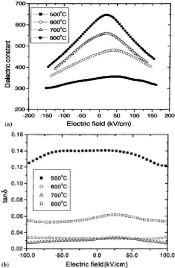
3.3.4 Dielectric properties
Figs. 3.18 (a) and (b) shows the variation of dielectric constant and the loss tangent with applied d.c.-electric field of the BST thin films annealed at different temperatures. With the increase in the annealing temperature the dielectric constant also increased. The 800℃ annealed thin film shows maximum dielectric constant of around 650 and that of the film annealed at 500℃ is the lowest, approximately 325 at zero bias. The electric field at which the dielectric constant has its maximum value is not located at the zero bias fields instead shifted towards the positive voltage region.
Maximum dielectric constant field (Em) has shifted consistently from 43 kV cm–1 for
500℃ annealed film to 20 kV cm–1 for the film annealed at 800℃. The increase in
dielectric constant with increasing annealing temperature is attributed to the increase in the grain size and crystallinity of the thin film. XRD and SEM results showed that with increasing annealing temperature, crystallinity and grain size increased, which in turn resulted in larger polarization density there by increasing the dielectric constant. It is well known that as the grain size increases the dielectric constant increases and as the porosity in the film increases, the dielectric constant decreases.
The shift in electric field at which the dielectric constant has its maximum is because of the same reason that changes in the interface characteristics brought in by annealing the film at different temperature and associated Ti-migration problem which modifies the interface. The space charge capacitance at the two interfaces is different because of the difference in interface characteristics. The dielectric loss is maximum for film annealed at 500℃ (0.14 at zero bias). Lowest loss tangent is observed for the BST films annealed at 600 and 700℃ (0.04). Also, these thin films
show approximately similar behavior under the bias field variation. Further increase in the annealing temperature to 800℃ resulted in the increase of loss tangent to higher value (0.06 at zero bias) than the film annealed at 600 and 700℃ but much lower than the film annealed at 500℃.
The dielectric loss originates from two mechanisms: resistive loss and relaxation loss. Resistive loss mechanism involves energy consumption by the mobile charges in the film; whereas, in the case of relaxation loss mechanism, it is relaxation of the dipole which dissipates the energy. If there is very few mobile charges in the film then the later mechanism is dominating. The resistive loss mechanism is directly connected to the leakage current of the film: if the leakage current is higher the loss is also higher. Alternatively, if the dielectric constant of the film is larger, then an increase in the dielectric loss is obvious due to the contribution from the second mechanism. Enhanced polarization increases the energy dissipation during the relaxation. The higher dielectric loss of 500℃ annealed film is due to the higher leakage current of the film. Lowest leakage current is observed for the films annealed at 600 and 700℃ hence a low dielectric loss. The increase in the loss tangent after annealing at 800℃ is due to the increased leakage current and also due to dipole relaxational loss because of the enhanced polarisation effect.
The capacitance-voltage (C-V) characteristics for the Ag-BST composite thin films are plotted in Fig. 3.19. No measurable capacitance could be recorded for 5 % Ag-doped BST film because of poor adhesion of the film with the substrate as revealed by cross-sectional SEM. The capacitance decreases, in general, with the increase in Ag content in the BST film.
In order to check whether the improved microstructure for 2 % Ag-doped BST leads to low loss characteristics, dielectric loss measured for 0%, 1%, 2%, 3% and 4%
Ag- doped BST composite films are compared in Fig. 3.20. The 2% Ag-doped BST has the lowest dielectric loss at 0 bias (0.02), which is ~4 times less than pure BST. Moreover, the loss remains nearly the same for the whole range of applied bias potential, which indicates that the less porous uniform microstructure of 2% Ag-doped BST has led to significant reduction in dielectric loss although the dielectric constant value is less than pure BST. The dielectric loss, however, increases with further increase in Ag content.
CHAPTER 4
CONCLUDING REMARKS
This three-year group research project has designed and established an experimental RTP (Rapid Thermal Processing) processor for a 12-inch single silicon wafer. According to these three individual projects, the major results obtained can be summarized in the following.
(1) Combining lamps and active multi-zone resistance heater can reduce the processing time and improve the wafer temperature uniformity.
(2) The absorptance of the BST/Si samples is higher than 60% in the range of 0.64 to
6 µm, and the absorptance of the samples increases with an increase in BST film
thickness in the spectral range 6-19.6 µm. By Beer’s law, the extinction coefficient of the BST films is high in the spectral range from 0.64 to 11 µm.
(3) Ba0.5Sr0.5TiO3 thin films can be deposited on the Pt/Ti/SiO2/Si substrate at a
low-temperature using complex precursor solution prepared by using hydroxides of Ba and Sr as the Ba-, Sr-sources, Ti-isopropoxide as the Ti-source and 2-methoxy ethanol as the solvent. Reasonably, good film with low leakage and high dielectric constant can be obtained after annealing above 700℃ wherein the embedded carbonations decomposition products must have been burnt-off. The leakage current characteristic and the dielectric constant depend on the processing parameters such as annealing temperature, film thickness and precursor concentration. Another important finding of the study is the microstructure can be tailored by changing the concentration of the precursor solution. As a whole, our study highlights the intricate relationship between the film processing, microstructure and the properties of the film. The dielectric constant decreases with increasing Ag content approximately according to the second order power
law dependence, and no measurable capacitance could be recorded for BST films with Ag content >6 %. Dielectric loss, which is four times less than pure BST, is recorded for the 2 % Ag-doped BST film because of the improvement in the microstructure.
REFERENCES
1. zturk, M. C., Sorrell, F. Y., Wortman, J. J., Johnson, F. S., and Grider, D. T., Manufacturability Issues in Rapid Thermal Chemical Vapor Deposition, IEEE Trans. of Semiconductor Manufacturing . Vol.4 No.2., 155-165 (1991)
2. Biber, C. R., Wang, C. A., and Motakef, S., Flow Regime Map and Deposition Rate in Vertical Rotating-Disk OMVPE Reactor, Journal of Crystal Growth 123, 545-554 (1992)
3. Wang, C.A., Groves, S.H., and Palmateer, S.C., Flow Visualization Studies for Optimization of OMVPE Reactor Design, Journal of Crystal Growth 77, 136-143 (1986)
4. Pollard, R., and Newman, J., Silicon Deposition on a Rotating Disk, J. Electrochem. Soc. Solid Stste Science and technology, Vol. 127, No.3,.744-752 (1980)
5. Gadgil, P. N., Optimization of a Stagnation Point Flow Reactor Design for Metalorganic Chemical Vapor Deposition by Flow Visualization, Journal of Crystal Growth 134, 302-312 (1993)
6. Gadgil, P. N., Single Wafer Processing in Stagnation Point Flow CVD Reactor: Prospects, Constrains and Reactor Design, Journal of Electronic Materials 22, No.2, 171-177 (1993)
7. Fotiads, D. I., and Kieda, S., Transport Phenomena in Vertical Reactors for Metalorganic Vapor Phase Epitaxy, Journal of Crystal Growth 102, 441-470 (1990)
8. Kleijn, C. R., Th. H. van der Meer, and Hoogendoorn, C. J., A Mathematical Model for LPCVD in a Single Wafer Reactor, J. Electrochem. Soc., Vol. 136, No. 11, 3423-3433 (1989)
9. Evans, G., and Grief, R., Effects of Boundary Conditions on The Flow and Heat Transfer in a Rotating Disk Chemical Vapor Deposition Reactor, Numerical Heat Transfer, Vol. 12, 243-252 (1987)
10. Moslehi, M. M., Velo, L., Ajit Paranjpt, Kuehne, J., Huang, S., Chapman, R., Schaper, S., Breedijk, B., Najm, H., Yin, D., Lee, Y. J., Anderson, D., and Davids, C., Fast-Cycle-Time Single-wafer IC Manufacturing, Microelectronic Engineering 25, 93-130(1994)
11. Reid, K. G. and Sitaram, A. R., High Temperature Thermal Processing for ULSI Application, Mat. Res. Soc. Symp. Proc. 387, 201-211(1995)
12. Detaton, R., and Massoud, H. Z., Effect of Thermally Induced Stresses on the Rapid Thermal Oxidation, J. Appl. Phys. 70(7),1, 3588-3592 (1991)
13. Lord, H. A., Thermal and Stress Analysis of Semiconductor Wafer in a Rapid Thermal Processing Oven, IEEE Trans. of Semiconductor Manufacturing . Vol.1 No.3, 105-114 (1988)
14. Sorrell, F. Y., Fordham, M. J., zturk, M. C., and Wortman, J. J., Temperature Uniformity in RTP Furances, IEEE Trans. of Electron Devices . Vol.39 No.1, 75-80 (1992)
15. Campbell, S. A., Kanutson, K. L., Liu, B. Y. H., and Leighton, J. D., Steady-State Thermal Uniformity and Gas Flow Pattern in a Rapid Thermal Processing Chamber, IEEE Trans. of Semiconductor Manufacturing . Vol.4 No.1, 14-19 (1991)
16. Nenyei, E., Sommer, H., Gelpey, J., and Bauer,A., Gas Flow Engineering in Rapid Thermal Processing, Mat. Res. Soc. Symp. Proc. 342, 401-406(1994) 17. Timans, P. J., Morishige, R. N., and Wasserman, Y., Emissivity-independent
Rapid Thermal Processing Using Radiation Shield, Mat. Res. Soc. Symp. Proc. 470, 57-62 (1997)
18. Young, G. L., and McDnald, K. A., Effect of Radiation Shield Angle on Temperature and Stress Profiles During Rapid Thermal Annealing, IEEE Trans. Semicond. Eanuf. 3 (4), 176-182(1990)
19. Cho B. J., and Kim, C. K., Elimination of Slip on Silicon Wafer Edge in Rapid Thermal Process by Using a Ring Oxide, J. Appl. Phys.,67(12), 7583-7586(1990)
20. Zollner, J. P., Patzschke, I., Pietzuch, V., Pezoldt, J.,and Eichhorn, G.,To The Influence of The Wafer Edge in RTP, Mat. Res. Soc. Symp. Proc. 303, 177-182 (1993)
21. Kakoschke, R., Bubmann, E., Simulation of Temperature Effects During Rapid Thermal Processing, Mat. Res. Soc. Symp. Proc. 146, 473-482 (1989)
22. Riley, T. J., and Gyurcsik, R. S., Rapid Thermal Processor Modeling, Control, and Design for Temperature Uniformity, Mat. Res. Soc. Symp. Proc. 303, 223-229(1993)
23. Kakoshke, R., Bubmann, E., and Foll, H., Modeling of Wafer Heating During Rapid Thermal Processing, Appl. Phys. A50(2), 141-150(1990)
24. Cho, Y. M., Paulraj, A., Kailath, T., and Xu, G. H., A Contribution to Optimal Lamp Design in Rapid Thermal Processing, IEEE Trans. Semicond. Manuf. 7(1), 34-41(1991)
25. Gongste, J. F., Oosterlaken, T. G. M., Bart, G. C. J. , Janssen, G. C. A. M., and Radelaar, S., Deformation of Si (100) Wafers During Rapid Thermal Processing, J. Appl. Phys. 75(6), 2830-2836(1994)
26. Lee, K. C., Chang, H. Y., and Hu, J. G., A New Temperature Compensation Method for SI Wafer in Rapid Thermal Processor Using Seperated SI Rings As Suspector, Res. Soc. Symp. Proc. 470, 187-192(1997)
Uniformity During Rapid Thermal Processing, Mat. Res. Soc. Symp. Proc. 224, 185-196(1991)
28. P. Vandenabeele, Maex, K., and Keersmaecker, R. D., Rapid Thermal Annealing / Chemical Vapor Deposition and Integrated Processing, Mat. Res. Soc. Symp. Proc. 146, 149-160(1989)
29. Hebb, J. P., Jensen, K. F., and Egan, E. W., The Potential Effect of Multilayer Patterns on Temperature Uniformity During Rapid Thermal Processing, Mat. Res. Soc. Symp. Proc. 387, 21-27(1995)
30. Thakur, R. P. S., Martin, A., Fackrell, W. T., and Barbour, R., Stress and Warpage Studies of Silicon and Patterned Films During Rapid Thermal Processing (RTP), Mat. Res. Soc. Symp. Proc. 303, 189-195(1993)
31. Hu, S. M., Stress-Related Problems in Silicon Technology, J. Appl. Phys., 70(6), R53-R80(1991)
32. Wong P. Y., and Miaoulis, I. N., Thermal-Radiation Absoraption Charactristics of Patterned Wafer During Rapid thermal Processing, Mat. Res. Soc. Symp. Proc. 342, 395-400(1994)
33. Chen, M. M., Berkowitz-Mattuck, J. B., and Glaser, P. E., The Use of a Kaleidoscope to Obtain Uniform Flux Over a Large Area in a Solar or Arc Imaging Furance, Appl. Optics 2, 265-271(1963)
34. Sheets, R. E., Temperature Measurement and control in a Rapid Thermal Processor, Mat. Res. Soc. Symp. Proc. 52, 191-197(1986)
35. Sheets, R. E., Automatic Cassette to Cassette Radiant Impulse Processor, Nucl. Instrum. Meth. Phys. Res., B6, 219-223(1985)
36. Norman, S. A., Schaper, C. D., and Body, S. P., Improvement of Temperature Uniformity in Rapid Thermal Processing System Using Multivariable Control, Mat. Res. Soc. Symp. Proc. 224, 177-183(1991)
37. Roozeboom, F., Temperature Control and System Design Aspects in Rapid Thermal Processing, Mat. Res. Soc. Symp. Proc. 224, 9-16(1991)
38. Schaper, C., Moslehi, M. M., Saraswat, K., and Kailath, T., Control of MMST RTP : Repeatability, Uniformity, and Integration for Flexible Manufacturing, IEEE Trans. of Semiconductor Manufacturing, Vol. 7, No. 2, 202-219(1994) 39. Gyursik, R. S., Riley, T. J., and Sorrell, F. Y., A Model for Rapid Thermal
Processing : Achieving Uniformity Through Lamp Control, IEEE Trans. of Semiconductor Manufacturing . Vol.4 No.1, 9-14 (1991)
40. Moslehi, M. M., Kuehne, J., Yeakley, R., Velo, L., Najm, H., Paranjpt, A., Dostalki, B., Yin, D., and Cecil, D., In-Situ Fabrication and Process Control Techniques in Rapid Thermal Processing, Mat. Res. Soc. Symp. Proc. 224, 143-157(1991)
41. Spence, P., Schaper, C., and Kermani, A., Concurrent Design of An RTP Chamber and Advanced Control System, Mat. Res. Soc. Symp. Proc. 387, 75-86(1995)
42. Apte, P. P., Wood, S., Booth, L., Saraswat, K. C., Moslehi, M. M., Temperature Uniformity Optimization Using Three-Zone Lamp and Dynamic Control in Rapid Thermal multiprocessor, Mat. Res. Soc. Symp. Proc. 224, 209-214(1991) 43. Hoyt, J. L.and Gibbons, J. F., Rapid Thermal Annealing of As in Si, Mat. Res.
Soc. Symp. Proc. 52, 15-22(1986)
44. Belikov, S., Temperature Estimation and Precision Control of RTP Systems By Multi-Zone Lamp Interference and Wafer Emissivity Compensation I : Model Identification, Mat. Res. Soc. Symp. Proc. 470, 91-96(1997)
45. Xu, H.,and Sturm, J. C., Effects of Reflective Surfaces on Silicon Emissivity and Temperature Measurements, Mat. Res. Soc. Symp. Proc. 429, 297-302(1996)
46. Schietinger, C., Adams, B., and Yarling, C., Ripple Technique ; A Novel Non-Contact Wafer Emissivity and Temperature Method for RTP, Mat. Res. Soc. Symp. Proc. 224, 23-30(1991)
47. Nguyenphu, B., Oh, M., and Fiory, A. T., Temperature Monitoring By Ripple Pyrometer in RTP, Mat. Res. Soc. Symp. Proc. 429, 291-296(1996)
48. Saraswat, K. C., Chen, Y., Degertekin, L., and Khuri-Yakub, B. T., A New Flexible Rapid Thermal Processing System, Mat. Res. Soc. Symp. Proc. 387, 35-47 (1995)
49. Burckel, D., Zaidi, S. H., and Brueck, S. R. J., Sub-Feature Speckle Interferometry : A New Approach to Temperature Measurement, Mat. Res. Soc. Symp. Proc. 387, 125-132(1995)
Table 3.1 Lattice parameter after annealing the thin film at different temperatures calculated using (1 1 0) reflection and Pt (1 1 1) peak as the standard
-15 -10 -5 0 5 10 15 140 150 160 X(cm) T(oC)
(a) t = 200s
, ∆T
max=2.1℃
-15 -10 -5 0 5 10 15 180 190 200 X(cm) T(oC)(b) t = 300s
, ∆T
max=2.58℃
-15 -10 -5 0 5 10 15 180 190 200 X(cm) T(oC)(c) t = 400s
, ∆T
max=3.31℃
-15 -10 -5 0 5 10 15 230 240 X(cm) T(oC)(d) t=500s
, ∆T
max=1.4℃
Fig. 3.3 The temperature distribution on the wafer at selected locations for
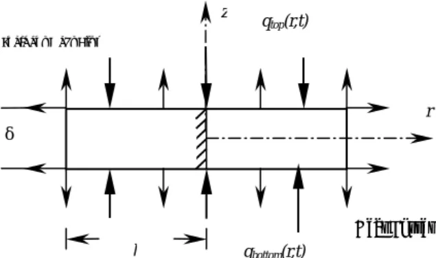
z
r Incident Heat Flux
l δ Heat Losses qbottom(r,t) qtop(r,t) (a) (b) (c)
Fig. 3.5 Inverse incident-heat-flux profiles results for a measurement error of
σ=0.0 at linear ramp-up rates of (a) 100oC/sec (b) 200oC/sec, and (c)
300oC/sec.
Fig. 3.4 Schematic representation of energy flux in a wafer under incident heat flux and radiant heat losses emitted from all surfaces.
(a)
(b)
(c)
Fig. 3.7 Resulting maximum temperature difference for measurement errors of
σ
=0.0,σ
=0.001,σ
=0.003 andσ
=0.005 as a function of the linearramp-up rate.
Fig. 3.6 Inverse incident-heat-flux thermal non-uniformity profile results for a
measurement error of σ =0.0 at linear ramp-up rates of (a) 100oC/sec, (b)
200oC/sec and (c) 300 oC/sec.
100 150 200 250 300
Linear Ramp-up Rate ( oC/sec )
0.7 0.8 0.9 1.0 1.1 1.2 1.3 1.4 1.5 1.6 Ma xi mu m
|
∆ T|
( o C ) σ = 0.0 σ = 0.001 σ = 0.003 σ = 0.0050 4 8 12 16 20 Wavelength (µm) 0 20 40 60 80 100 Tr an sm ittan ce (% )
thin film thickness 0.17 µm thin film thickness 0.4 µm thin film thickness 0.52 µm
0 4 Wavelength (8 12µm) 16 20 0 20 40 60 80 100 Re flec tan ce (%)
thin film thickness 0.17µm thin film thickness 0.4µm thin film thickness 0.52µm
0 0.2 0.4 0.6 0.8 Wavelength (µm) 1.6 2 2.4 2.8 3.2 3.6 Re fr act iv e i nde x , n film thickness 0.17µm film thickness 0.4µm film thickness 0.52µm 0 0.2 0.4 0.6 0.8 Wavelength (µm) 0 0.4 0.8 1.2 1.6 Ab so rp tive in de x , k film thickness 0.17µm film thickness 0.4µm film thickness 0.52µm 0 5Wavelength (10 µ15m) 20 0 20 40 60 80 100 R ef le ct an ce (% ) Si/BST 30 oC 100 oC 200 oC 300 oC 400 oC 500 oC 600 oC 678 oC
Fig. 3.9 Variation of reflectance as a function of wavelength for different thickness of the BST thin
Fig. 3.10 The refractive index of the BST thin films for different thickness.
Fig. 3.11 The absorption index of the BST thin films for different thickness. Fig. 3.8 Variation of transmittance as a
function of wavelength for different thickness of the BST thin films.
Fig. 3.12 Variation of reflectance as a function of wavelength for different temperature of the BST thin films.
Fig. 3.13 Variation of the thickness of the 500℃ pyrolysed film after annealing at different temperatures determined using SEM cross-sectional image.
Fig. 3.14 SEM (a) surface and (b) cross-sectional image of Pt/Ti/SiO2/Si wafer after annealing at 800℃ for 2 h showing the TiOx islands on the surface of Pt film formed by the migration of Ti through the Pt-grain boundaries. The
thickness of the interfacial layer formed is about 128 nm.
Fig. 3.15 J–E plot of BST thin films post-annealed at different temperatures for 2 h in air.
Fig. 3.16 Verification of the second order power dependence of the leakage current density at 100 kV/cm (J100 kV/cm) against the Ag content in the BST films
according to percolation theory for a metal-dielectric composite.
-1 0 1 2 3 4 5 6 7 10-7 10-6 10-5 10-4 10-3 10-2 10-1 Curv e Equation: Y = -6.61617 - 0. 34183 X+ 0. 17315 X2 Ag(6)-BST Critical concentration Ag(4)-BST Ag(3)-BST Ag(2)-BST Ag(1)-BST Ag(0)-BST Lea kage c ur rent d ens ity ( J 100 k V/c m A/ cm 2) Ag Content (Mole %)
Fig. 3.17 J–E plot of BST thin films prepared from precursor solutions ofthree different concentrations and post-annealed at 700℃ per 2 h in air.
Fig. 3.18 (a) Variation of the 100 kHz dielectric constant with applied electric field for the BST thin films annealed at different temperatures for 2 h in air and (b) Variationof the loss tangent with applied electric field for the BST thin
films annealed at different temperatures for 2 h in air.
Fig. 3.19 Capacitance vs. Voltage characteristics for Ag (0, 1, 2, 3, 4, 6)-BST thin films.
Fig. 3.20 Comparison of dielectric loss measured for 2 % Ag-doped BST (Ag(2)-BST) film with the loss characteristics recorded for 0, 1, 3 and 4 %-Ag-doped
-6 -4 -2 0 2 4 6 2.0x10⁻¹⁰ 2.4x10⁻¹⁰ 2.8x10⁻¹⁰ 3.2x10⁻¹⁰ 3.6x10⁻¹⁰ 4.0x10⁻¹⁰ 4.4x10⁻¹⁰ 4.8x10⁻¹⁰ 5.2x10⁻¹⁰ 5.6x10⁻¹⁰ 6.0x10⁻¹⁰ 0% Ag 1% Ag 2% Ag 3% Ag 4% Ag 6% Ag C apac itanc e ( F ) Voltage (V) -6 -4 -2 0 2 4 6 0.01 0.1 1 10 0% Ag 1% Ag 2% Ag 3% Ag 4% Ag D iel ec tr ic Los s Voltage (V)