國 立 交 通 大 學
電子工程學系 電子研究所碩士班
碩士論文
形成矽化鎳時在矽化鎳與矽接面處離子活化相關研究
Research of Dopant Activation at the Interface
between Nickel Silicide and Silicon during Nickel
Silicide Formation
研 究 生:孫成業 Student:Cheng-Yeh Sun
指導教授:張國明 博士 Advisor:Dr. Kow-Ming Chang
桂正楣 博士 Dr. Cheng-May Kwei
形成矽化鎳時在矽化鎳與矽接面處離子活化相
關研究
Research of Dopant Activation at the Interface
between Nickel Silicide and Silicon during Nickel
Silicide Formation
研 究 生:孫成業 Student:Cheng-Yeh Sun
指導教授:張國明 博士 Advisor:Dr. Kow-Ming Chang
桂正楣 博士 Dr. Cheng-May Kwei
國 立 交 通 大 學
電子工程學系 電子研究所碩士班
碩 士 論 文
A ThesisSubmitted to Institute of Electronics
College of Electrical Engineering and Computer Science National Chiao Tung University
In Partial Fulfillment of the Requirements for the Degree of
Master of Science In
Electronics Engineering
September 2006,
Hsinchu, Taiwan, Republic of China
中華民國九十五年九月形成矽化鎳時在矽化鎳與矽接面處離子活化相
關研究
研究生:孫 成 業 指導教授:張 國 明 博士 桂 正 楣 博士 國 立 交 通 大 學 電子工程學系 電子研究所碩士班摘要
在先進互補式金氧半導體元件裡,當接觸尺寸縮小至奈米等級,源極及汲極 的接觸電阻也會隨之增加。因此,金屬矽化物的技術應用在源極及汲極已經被開 發用來同時降低接觸電阻及接面寄生電阻。在奈米金氧半場效電晶體的製造中, 矽化製程是必須的,為了抑制源極及汲極的超淺接面形成所產生的短通道效應。 所以,是否具有與矽基材完好介面特性的金屬矽化物,是在製造奈米尺寸的元件 時重要的製程考量。在本論文中,我們主要探討離子佈植入矽化鎳再經由後續不 同條件的退火製程後,所呈現出的活化量及電特性的研究。吾人實驗結果顯示矽 化鎳經兩階段退火有助於介面狀態的改善,並且使活化的摻雜物朝介面堆積,接 面呈現歐姆接觸(Ohmic Contact)。但是硼摻雜物當退火溫度超過550 ℃ 30 sec 會發生短暫增強擴散(Transient Enhanced Diffusion)使硼向矽基材擴散,磷摻雜物 則有不會發生此種現象。具有較強的溫度免疫力,可適用於高溫製程。硼則是具 有較好的低溫活化能力。Research of Low Temperature Activation Nickel Silicide and
Interface properties
Student:Cheng-Yeh Sun Advisor:Dr. Kow-Ming Chang Advisor:Dr. Cheng-May Kwei
Department of Electronics Engineering and Institute of Electronics
National Chiao Tung University
Abstract
In advanced CMOS devices, as contact dimensions scale down to nanometer range, contact resistance of source and drain is increased correspondingly. As a result, the technique of metal silicides for poly gate and source/drain has been developed to reduce the contact resistance and the parasitic junction resistance as well. In nanometer MOSFET fabrication, this silicidation process requires considering to suppress short channel effect (SCE) when forming the ultra shallow source and drain junction. Therefore, metal silicides owning a perfect interfacial property with Si above an ultra-shallow junction is considered as a critical module toward the realization of nano-scale CMOS. In the thesis, we want know the amount of activation and electro-characteristics by different thermal process. The experiments show that nickel silicide interface state
activation dopant accumulates toward the interface. The junction presents ohmic contact. The implanted boron sample occur transient enhanced diffusion result in boron diffuse toward silicon substrate above 550 ℃ 30 sec. This phenomenon does not occur in the implanted phosphorous sample. Has the strong temperature immunity, suitably in high temperature process. However the boron has good activation ability at low temperature.
誌 謝
南風又輕輕的吹起,絲絲的離情充滿了整個校園,艷麗的鳳凰花悄悄在枝頭 綻放,昔日的讀書聲,窗外的嬉笑聲,也將成為美麗的回憶,想到這裡內心是多 麼沉重,一股股的心酸不時的湧上心頭。 回憶兩年來在交大電子的學習生活,首先感謝指導教授張國明教授與桂正楣 教授在課業上給我的諄諄教誨以及鼓勵,指導我的碩士論文研究,老師您就像是 辛勤的園丁,我們就像含苞待放的花朵,如今我們盛開了,今日的成果要感謝老 師的諄諄教誨,我們將永遠長記心中。 同時也要感謝許許多多的碩士班學長、同學及學弟。另外特別感謝一直指導 我的林建宏學長,不論是在實驗上,最後論文的修訂,準備口試時提供的建議及 幫助,使我論文能夠盡善盡美。還有感謝交大奈米中心、國家奈米實驗室提供各 種實驗設備,可以讓我順利進行實驗。 最後要感謝我的家人,媽媽、哥哥、姐姐以及女友,沒有你們的支持與鼓勵 我也沒辦法順利考上交大電子,完成碩士學位,最後,感念我的父親,相信他會 以我為榮的。Contents
Chinese Abstract ··· i
English Abstract ··· ··· ii
Acknowledgements··· iv
Contents ··· v
Table Captions ··· vii
Figure Captions ··· viii
Chapter 1 Introduction ··· 1
1.1 General background ··· 1
1.2 Motivation ··· 4
1.3 Organization of thesis··· 5
1.4 References ··· 6
Chapter 2 Formation and Characterization of Boron/Phosphorous Implanted Through Silicide by Subsequence Thermal Process··· 8
2.1 Introduction ··· 8
2.2 Experiment ··· 11
2.3 References ··· 12
Chapter 3 Physical Properties and Electrical Characteristics of Boron/Phosphorous Implanted Through Silicide··· 14
3.1.1 Surface morphology by AFM inspection ··· 14
3.1.2 SEM cross-sectional view inspection··· 15
3.2 Electrical measurements··· 15
3.2.1 I-V measurement ··· 15
3.2.2 Reverse leakage current density··· 17
3.2.3 C-V measurement and doping profile extraction ··· 18
3.3 References··· 22
Chapter 4 Conclusion··· 24
Table Captions Chapter 1
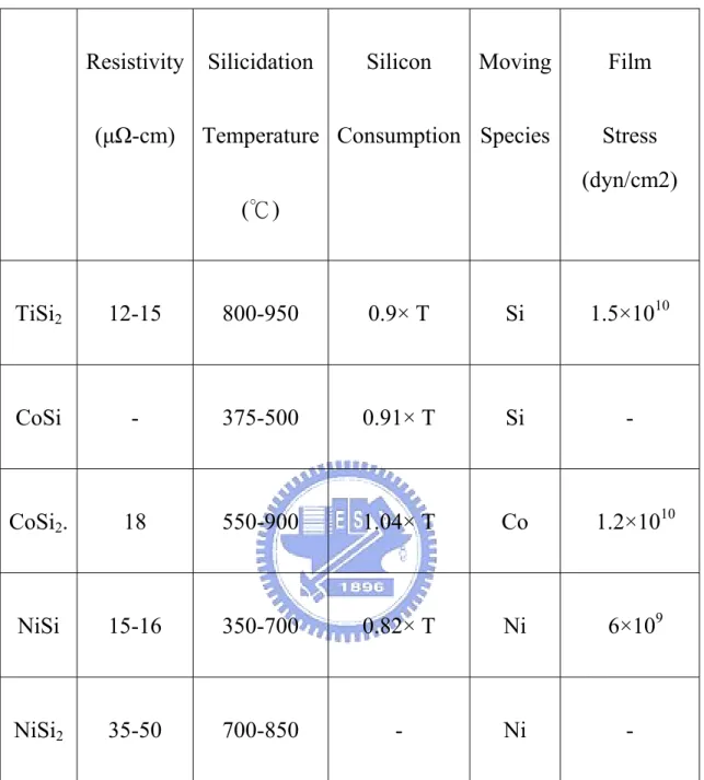
Table 1-1 Comparison the characteristics of Ti, Co and Ni silicides.
Chapter 2
Figure Captions Chapter 1
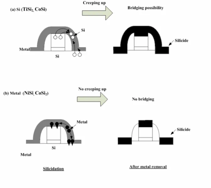
Fig 1-1 With/without creep up phenomenon of metal silicides.
Chapter 2
Fig. 2-1 Process flow of NiSi/p+p junction by ITS scheme.
Chapter 3
Fig. 3-1 AFM image shows NiSi/Si interface morphology by 2nd RTP annealing (a) 400 ℃ (b) 500 ℃ (c) 600 ℃ (d) 700 ℃ for 30 sec.
Fig. 3-2 RMS value of the interface roughness versus temperature with / without 2nd RTP annealing.
Fig. 3-3 SEM image shows NiSi formed by RTP annealing 400 ℃ for 30 sec.
Fig. 3-4 Four basic transport process under forward bias. [1]
Fig. 3-5 The ID-VD characteristic curves of the NiSi/Si junction diode
without 2nd RTA by (a) BF2 +
Fig. 3-6 The forward ID-VD characteristic curves of the NiSi/Si junction
diode with 2nd RTA 30 sec by (a) BF2 +
implantation and (b) P+ implantation.
Fig. 3-7 The ID-VD characteristic curves of the NiSi/Si junction diode
with 2nd RTA 30 sec by (a) BF2 +
implantation and (b) P+ implantation.
Fig. 3-8 The forward bias current density versus annealing temperature for the NiSi / Si junction diodes fabricated with (a) BF2+ and (b) P+
implantation at various annealing time.
Fig. 3-9 The reverse bias current density versus annealing temperature for the NiSi / Si junction diodes fabricated with (a) BF2+ and (b) P+
implantation at various annealing time.
Fig. 3-10 The capacitance-voltage characteristics of Schottky junction diodes implanted (a) BF2+ and (b) P+ without 2nd RTA.
Fig. 3-11 The doping concentration versus depth for the implanted (a) BF2
+
and (b) P+ by annealing at various temperature.
Fig. 3-12 The Active charge versus anneals temperature for (a) Boron and (b) Phosphorous implant.
Chapter 1
Introduction
1.1 General background
In order to improve the performance and packing density of metal-oxide-semiconductor (MOS) integrated circuit, the device dimension has been scaled down to nanometer region. In nanometer complementary metal- oxide- semiconductor (CMOS) circuit with gate length down to 0.1 µm, the parasitic resistance of gate, source and drain region will increase. Result in the increase of RC time delay and more power dissipation with integrated circuit.
In past years, many people effort to develop a new technology for reducing parasitic resistance to improve the device and circuit performance. Recently, the metal-silicide-related technology has become an integral part of nanometer devices for reducing the parasitic resistance in order to improve the devices and circuit performance. The major advantages of metal silicides can be grouped as follows:
formation by self-aligned technology without any extra mask and compatible with conventional CMOS process.
Where the self-aligned silicide (salicide) process is widely used in MOS manufacturing to reduce the sheet resistance and contact resistance of the gate polysilicon. [1] In nanometer MOSFET fabrication, this silicidation process requires considering to suppress short channel effect (SCE) when forming the ultra shallow source and drain junction. Therefore, metal silicides owning a perfect interfacial property with Si above an ultra-shallow junction is considered as a critical module toward the realization of nano-scale CMOS. Besides, as the oxide thickness scaling down with the device dimensions, the gate oxide reliability will also be a concern for the silicided gate process.
Recently, numbers of silicide have been discussed to use to improve device performance, such as TiSi2, CoSi2, MoSi2 and NiSi. Some of
silicide, TiSi2, CoSi2 and NiSi, has been used IC process. However,
different silicide could observe different characteristics. Some properties have good merits for device fabrication, but some ones would affect the integrity circuit processes.
Titanium disilicide (TiSi2) has been the most commonly used
metal-silicide in ULSI process. Then, TiSi2 must be phase transformation
from the high resistivity phase C49 to low resistivity phase C54 [2-3].As line keeps below 0.2 µm, the width of C49-TiSi2 is not enough to
complete conversion to C54-TiSi2 ( 800 ) structure and the silicide ≧ ℃
also a problem of TiSi2 process. During the silicidation of Ti/Si system,
the Si atom is the dominant diffusing species. This facilitates the problem of creep-up in the MOSFET salicide structure, silicidation may occur on the side-walls, as shown in Fig 1.1. The possibility of Silicide Bridge forming between the gate and source or drain increases when creep-up is significant. As a consequence, there is an increasing need for new silicide material suitable for nanometer CMOS devices.
Cobalt disilicide (CoSi2) is another alternative because CoSi2 can be
formed on narrow lines without the phase transformation problem and it has line width-independent sheet resistance. [4-5] However, CoSi2 have
major drawbacks. The formation of CoSi2 consumes a relatively large
amount of Si compared to the other silicides, as show in Table 1.1. Moreover, non-uniform CoSi2/Si interface or Co spike will lead to the Increase of junction leakage. [6-7]This will be restricting the vertical scaling for CoSi2 to achieve shallow junction.
Recently, nickel monosilicide (NiSi) has received more attention over the last years. Because of it has lower resistivity, lower Si consumption than TiSi2 and CoSi2. Moreover, the film stress of NiSi is also much
lower than that of TiSi2 andCoSi2.
NiSi has another important advantage: reducing creep-up phenomenon. In the case of NiSi, silicidation proceeds by the diffusion of metal into the Si. So it can great amount reducing creep-up phenomenon. Recently, the work function of NiSi can be modulated by doping different dopants,
such as boron, arsenic. [8] These properties make NiSi suitable for nanometer CMOS technology.
NiSi has been widely used in industry. However, the problems encountered in the NiSi silicidation process are anomalously large junction leakage current and sheet degradation. Recently, using Ti or TaN cap [9] and nitrogen-doped [10] techniques have been reported to reduce junction leakage current. Ti or TaN cap structure on the Ni deposition can an excellent oxygen scavenger and improve the large junction leakage during the thermal process.
1.2 Motivation
The rapid advance of integrated circuit technology has moved the minimum feature size into nanometer region. The vertical dimension also needs to be shrunk so as to improve the characteristics of device. Thus, reducing the junction depth becomes critical for advanced CMOS devices. Shallow junctions are hard to achieve because the ion implantation process will produce the implanted dopant profile to a given depth. Furthermore, the lateral spreading resistance and contact resistance of a shallow junction are often too large. [11]; as a result, the speed of device may be slowed down by the parasitic resistance. This problem can be alleviated by metallizing the source/drain junction with silicide. However, the quarter-micron device requires a junction depth of less than 0.1 µm and the silicidation of such a shallow source/drain junction will consume a good part of the high doping regions. The major obstacle for the silicidation of ultra shallow junctions comes from the nonuniform
silicide/silicon interface which may lead to local spiking of the junction. Consequently, the junction leakage may increase enormously after the silicidation process. To avoid this problem, the silicide film must be much thinner than the junction depth.
In this thesis, we want to investigate the activation of B and P implant through silicide (ITS). We clarified the thermal budge required for deactivation of B/P and also showed the impact of this phenomenon on achieving a shallow junction with a low sheet resistance.
1.3 Organization of the Thesis
In this thesis, we concentrate our efforts on the activation of B and P implant through silicide by RTA process. In chapter 1, brief introduction metal-silicide technology history evolution. In chapter 2, first overview of metal-silicide technology is given to describe the various applications and process technologies. Second the process flow of fabrication will be described.
In chapter 3, the detail discussion of characteristics includes physical properties, electrical properties, current transport mechanism, doping profile extraction and temperature effect. In chapter 4 is conclusions and chapter 5 is future works.
1.4 References
[1] Anne Lauwers, An Steegen Muriel de Potter, Richard Lindsay, Alessandra Satta, Hugo Bender, and K. Maex, American Vacuum Society B 19(6) (2001).
[2] J.B. Lasky, J. S. Nakos, O. J. Cain, and P. J. Geiss, IEEE Trans, Electron Device 38, 262 (1991).
[3] K. Maex, Mater. Sci, Eng. R11, 53 (1993).
[4] A. E. Morgan, E. K. Broadbent, M. Delfino, B. Coulman, and D. K. Sadana, J. Electrochem. Soc. ,vol.134, no. 4, p. 925 (1987).
[5] Q. F. Wang, K. Maex, S. Kubicek, R .Jonckheere, B. Kerkwijk, and R. Verbeeck, VLSI Tech. Dig. Tech. Paper, p. 17 (1995).
[6] B. S. Chen, and M. C. Chen, “Formation of Cobalt silicided Shallow Junction Using Implant Into/Through Silicate Technology and Low Temperature Furnace Annealing,” IEEE Trans.Electron Devices, vol. 43, no. 2, pp. 258-266, Feb. (1996).
[7] K. Goto, J. Watanabe, T. Sukegawa, A. Fushida, T. Sakuma, and T. Sugii, “A Comparative Study of Leakage Mechanism of Co and Ni Salicide Processes,” IEEE Annual International eliability Physics Symposium, pp. 363-369, (1998).
VLSI Technology Digest of Technical Papers, 9A-3, (2005).
[9] T. Ohguro, T. Morimoto, Y. Ushiku, and H. lwai,“Analysis of enormously large junction leakage current in nickel-silicided n-type diffused layers and its improvement,”in Ext. Abst. SSDM, p. 192, (1993).
[10] T. Ohguro, S. Nakamura, E. Morifuji, M. Ono, T. Yoshitomi, M. Saito, H. S. Momose, and H. Iwai,“Nitrogen-doped nickel monosilicide technology for deep submicron CMOS salicide,”in IEDM Tech. Dig., p. 453, (1995).
[11] K. K. Ng, and W. T. Lynch, “The impact of intrinsic series resistance on MOSFET scaling,”IEEE Trans. Electron Device, vol. 34, p. 503, (1987).
Chapter 2
Formation and Characterization of Boron/Phosphorous Implanted Through Silicide by Subsequence Thermal Process
2.1 Introduction
As device dimension is scaled down to deep submicron, not only the
size of gate electrode is shrunk, but also the vertical dimension of doped source/drain regions must be scaled to avoid device punch through and short channel effects. In the past, pn junctions were formed by dopant ion implantation into Si substrate followed by high temperature furnace annealing for dopant activation and implantation damage annihilation. However, channeling effect and high temperature dopant diffusion limit the formation of shallow junction. This is particularly important for the p+n junction because boron is a light element and diffuses fast in silicon. In recent years, many advanced junction formation techniques have been studied using low energy ion implantation, low temperature annealing, and rapid thermal annealing process. These new methods are briefly reviewed as follows.
(1) Pre-amorphization of silicon substrate before dopant implantation Pre-amorphization has been widely used to control the channeling
behavior of implanted dopant atoms. After the pre-amorphization of the silicon substrate surface layer, dopant implantation was performed followed by crystal regrowth and annealing process for the junction formation. Many heavy atoms have been used as pre-amorphization species, such as Si [1] and Ge. [2-3] Solid phase epitaxial (SPE) scheme can be used to regrow the crystal from the amorphous layer at a temperature as low as 550 ℃ [4]. The growth rate depends on the element used for pre-amorphization as well as the dopant implanted following the pre-amorphization. A careful annealing process is needed to annihilate the massive defects and dislocation induced by the pre-amorphization.
(2) Elevated source/drain structure
This method is to raise the source/drain regions by depositing a polysilicon (poly-Si) or amorphous silicon (α-Si) film or growing a selective epitaxial Si or SiGe layer. [5-6] Deposition of poly-Si/α-Si film on the source/drain regions needs an additional lithographic step to define the elevated regions, while the selective epitaxial growth of silicon on the source/drain regions does not need such an additional lithographic step. The elevated source/drain regions made with selective epitaxial growth (SEG) provide a sacrificial layer for silicide formation and an alternative approach for the salicide process. However, the SEG scheme needs a high deposition temperature to obtain good crystallinity in the epitaxial layer. The fact that high temperature process deteriorates the device performance is the main disadvantage of this method. [7]
(3) Low energy ion implantation [8-10]
This is an extension of the conventional ion implantation technique. The implantation energy is lower than 1 keV and the implantation dose is typically from 1×10¹⁴ to 5×1014 cm-2. The major disadvantage of this method is that no commercial implantation system of such a low energy beam line is available for high throughput mass production with reasonable cost.
(4) ITS/ITM technique
The implant through silicide (ITS) and implant through metal (ITM) processes have been investigated for shallow junction formation. The ITS/ITM process consists of implanting dopants into/through silicide or metal layer and the subsequent thermal annealing to form a silicide-contacted shallow junction [11-14]. The ITS scheme in particular is of much benefit to the formation of shallow junction. This is because metal silicides have a larger nuclear stopping power than silicon for the implanted dopant ions and thus can reduce the channeling effect; in addition, the junction formed by the ITS scheme can be almost free of implant damage, which is mostly confined in the silicide layer. Thus, the post-implant annealing temperature can be lowered while shallow junctions with superb characteristics can be obtained. Moreover, the silicided junction is conformal to the silicide/silicon interface, and thus the possibility of junction penetration by the silicide is reduced.
Boron is used for the extension and source/drain regions of pMOSFETs. Boron offers a high solid solubility, [15-17] which produces
a low resistance, but has a relatively high diffusion coefficient that results in deep junctions. Both the solid solubility and the diffusion coefficient increase with temperature. Therefore, it is difficult to realize a low resistance and shallow junction when using B. For these problems, we employ the ITS scheme which is used for silicide-contacted shallow junction formation.
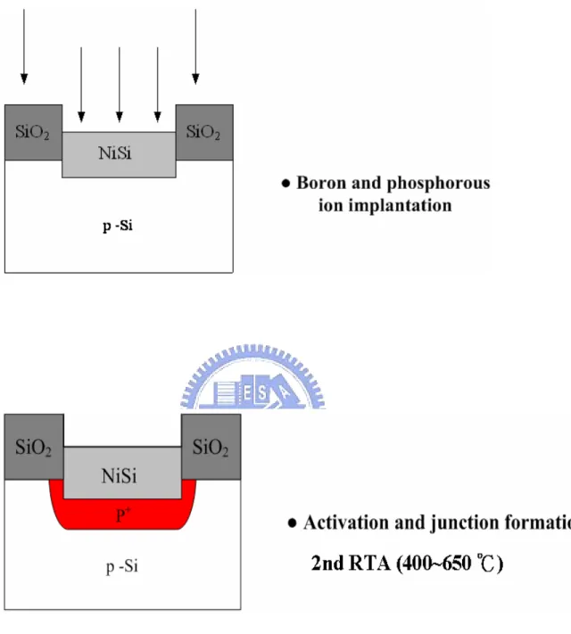
2.2 Experiment
Samples were fabricated on p-type (100) oriented Si wafers. After a standard RCA clean process. Then, a 400 nm isolation oxide was grown on the wafer by wet oxidation at 1050 for 30 min. The active regions ℃ were defined by the photolithography and etched by BOE (buffered oxide etchant) solution. Next, standard clean was used again to fully remove the contamination. Following, a 200 Å Ni deposited on the wafer in a dc sputtering system with a base pressure of less than 2.5×10⁻⁶ torr, using a Ni target in Ar ambient at a pressure of 2×10⁻³ torr with a deposition rate of about 0.1- 0.2 Å/sec. After the Ni film deposition, the samples were rapid thermal annealed (RTA) at 400 for 30 sec in N℃ 2 ambient to form
NiSi. The unreacted Ni film was selectively etched using a solution of H2SO4 : H2O2 = 3 : 1 at 75~85 for 60 sec. The formed NiSi film ℃
thickness was determined by cross-sectional scanning electron microscopy (SEM). Then, the sample of NiSi were implanted with BF2+ /
for 30 / 60 / 90 sec in N2 ambient for the activation dopant, as shown in
Fig 2-1. Process recipe is listed in table 2-1.
2.3 References
[1] M. H. Juang and H. C. Cheng, Appl. Phys. Lett. 60, 2092, (1992).
[2] M. C. Ozturk, J. J. Wortman, C. M. Osburn, A. Ajmera, G. A. Rozgonyi, E. Frey, W.-K. Chu, and C. Lee, IEEE Trans. Electron Devices 51, 663, (2004).
[3] K. Suzuki, H. Tashiro, K. Narita, and Y. Kataoka, IEEE Trans. Electron Devices 35, 659, (1988).
[4] M. Y. Tsai and B. G. Streetman, J. Appl. Phys. 50, 183, (1979).
[5] H. J. Huang, K. M. Chen, T. Y. Huang, T. S. Chao, G. W. Huang, C. H. Chien, and C. Y. Chang, IEEE Trans. Electron Devices 48, 1627, (2001).
[6] J. J. Sun, J. Y. Tsai, and C. M. Osburn, IEEE Trans. Electron Devices 45, 1946, (1998).
[7] K. Miyano, I. Mizushima, A. Hokazono, K. Ohuchi, Y, Tsunashima, IEDM Tech Digest, p. 433, (2000).
[8] Y. V. Ponomarev, P. A. Stolk, A. C. M. C. Van Brandenburg, C. J. J. Dachs, M. Kaiser, A. H. Montree, R. Roes, J. Schmitz, and P. H. Woerlee, VLSI Tech. Digest, p. 65, (1999).
[9] D. Kirkwood, A. Murrell, E. Collart, P. Banks, R. Fontaniere, and C. Maleville, IEEE International Conference on Ion Implantation Technology, p. 633 , (2002).
[10] A. Nishida, E. Murakami, and S. Kimura, IEEE Trans. Electron Devices 45, 701, (1998).
[11] C.-Y. Lu, J. J. Sung, R. Liu, N.-S. Tsai, R. Sing, S. J. Hillenius, and H. C. Kirsch, IEEE Trans. Electron Devices 38, 246, (1991).
[12] Q. Wang, C. M. Osburn, C. A. Canovai, IEEE Trans. Electron Devices 39, 2486, (1992).
[13] R. Angelucci, S. Solmi, A. Armigliato, S. Guerri, M. Merli, A. Poggi, and R. Canteri, J. Appl. Phys. 69, 3962, (1991).
[14] B. S. Chen and M. C. Chen, IEEE Trans. Electron Devices 43, 258, (1996).
[15] F. A. Trumbore, “Solid solubilities of impurity elements in germanium and silicin,”Bell Syst. Tech. J.,vol. 39, pp. 205-233, (1960).
[16] G. L. Vick, and K. M. Whittle, “Solid solubility and diffusion coefficients of boron in silicon,”J. Electrochem. Soc., vol. 116, pp. 1142-1144, (1969).
[17] G. Binning, C. F. Quate and Ch. Gerber, Phys. Rev. Lett., 56, p. 930, (1986).
Chapter 3
Physical Properties and Electrical Characteristics of Boron/Phosphorous Implanted Through Silicide
3.1 Physical Properties boron/ Phosphorous implantation through silicide
3.1.1 Surface morphology by AFM inspection
In 1986, Binning et al. introduced another apparatus for surface characterization in atomic scale, the atomic force microscope (AFM). Since it can be applied to any types of material and environment, AFM has thus been used widely in surface characterization. Owing to its atomic scale resolution capability, AFM is also powerful equipment for nano-structure fabrication.
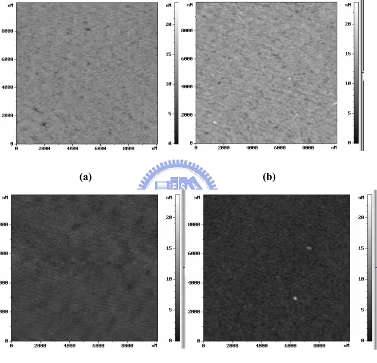
We want to inspect the surface morphology of NiSi/ Si interface by AFM. Because of the roughness between the NiSi/ Si interface related to the junction leakage. We want to know the impact on roughness of temperature.
Fig. 3-1 AFM image shows NiSi/Si interface morphology by 2nd RTP annealing (a) 400 (b) ℃ 500 ℃(c) 600 ℃ (d) 700 for 30 sec. Fig. 3℃ -2
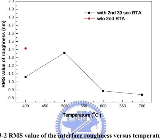
RMS value of the interface roughness versus temperature with / without 2nd RTP annealing. For the 2nd annealing sample, the interface roughness is smoother than the without 2nd annealing sample. Therefore 2nd annealing may improve interface roughness.
3.1.2 SEM cross-sectional view inspection
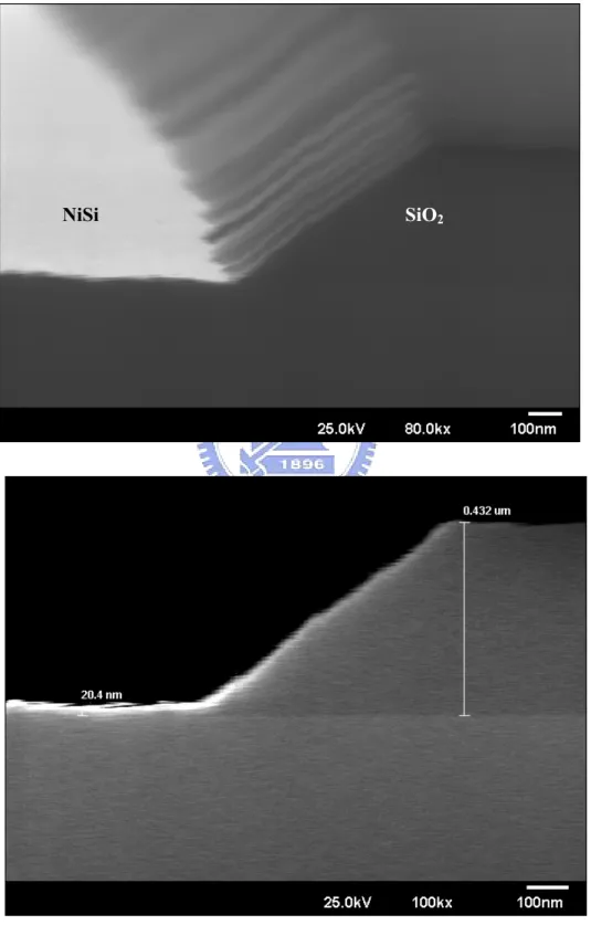
In order to identify the real thickness of the as-deposited Ni film and the NiSi layer formed, scanning electron microscope (SEM) was used for cross sectional view inspection. Fig. 3-3 shows SEM image of NiSi layer formed by RTP annealing at 400 for 30sec.℃
3.2 Electrical measurements
The electrical properties of the silicide-contacted shallow junction diodes fabricated by the ITS scheme are dependent on a number of factors, including the dopant activation level, implantation damage recovery, silicide/silicon interface roughness, and the distance between the silicide/silicon interface to the junction position. All of these are closely related to the energy and dosage of the dopant ion implantation as well as the dopant activation ability and the drive-in diffusion during the subsequent annealing process; this is especially important for the case of low thermal budget and low energy implantation for the ITS scheme.
The current transport in metal-semiconductor contacts is mainly due to majority carriers, in contrast to p-n junction, where the minority carriers are responsible. Fig. 3-4 shows four basic transport processes under forward bias.
The four processes are (1) transport of electrons form the semiconductor over the potential barrier into the metal[the dominate process for Schottky diodes with moderately doped semiconductors (e.g., Si with ND ≤ 1017
cm-3) operated at moderate temperatures(e.g., 300 °K)], (2) quantum-mechanical tunneling of electrons through the barrier (important for heavily doped semiconductors and responsible for most ohmic contacts), (3) recombination in the space-charge region [identical to recombination process in a p-n junction] and (4) hole injection from the metal to the semiconductor (equivalent to recombination in the neutral region). [1]
Fig. 3-5 shows the ID-VD characteristic curves of the NiSi/Si junction
diode without 2nd RTA by (a) BF2+ implantation and (b) P+ implantation.
It is obvious that the NiSi/Si junction stills to appear the Schottky junction behavior both the BF2+ and P+ implantation. The current
transport leads by majority carriers from semiconductor over potential barrier into the metal.
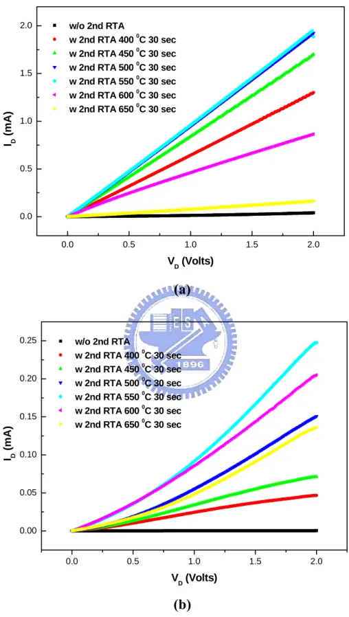
Fig. 3-6 shows the forward ID-VD characteristic curves of the NiSi/Si
junction diode with 2nd RTA 30 sec by (a) BF2+ implantation and (b) P+
implantation. We after discovered the curve presents the ohmic contact the linear curve to pass through 2nd RTA 30 sec. The forward currents rise
along with the annealing temperature. After 550 ℃ maximize starts to reduce along with the temperature rise. According to the extrapolation: NiSi/Si interface damage is recovered and roughness repaired at 550 ℃~650 ℃. Fig. 3-7 shows ID-VD characteristic curves of the NiSi/Si
junction diode with 2nd RTA 30 sec by (a) BF2+ implantation and (b) P+
implantation. The ID-VD characteristic curves approximate linear. We
knew schottky contact turns ohmic contact after the annealing process. Fig. 3-8 Forward bias current density versus annealing temperature for the NiSi/Si junction diodes fabricated with (a) BF2+ and (b) P+
implantation at various annealing time. Forward bias current density drops along with the time and the temperature rise. High temperature and long time RTA process may promote interface state. Cause the tunneling current is reduction. [2-3]
3.2.2 Reverse leakage current density
Fig. 3-9 shows the reverse bias current density (JR) versus annealing
temperature for the NiSi / Si junction diodes with an area of 0.000625 cm2 (250 × 250 µm) measured at a reverse bias of -5 V. The reverse bias current density (JR) is determined by directly dividing the measured
current by the diode’s area. Roughness of the silicide/Si interface in a shallow junction may lead to the formation of localized Schottky contacts or the agglomeration-induced local silicide spiking, resulting in the increase of reverse bias current. After annealing at temperature above 600
℃ 60 sec and above 500 ℃ 90 sec, the increased activation level, damage recovery level, and interface doping concentration should all have should all have contributed to better junction characteristics. [4]
3.2.3 C-V measurement and doping profile extraction
The capacitance-voltage (C-V) technique relies on the fact that the width of a reverse-biased space-charge region (scr) of a semiconductor junction device depends on applied voltage. This scr width dependence on voltage lies at the heart of the C-V technique. The C-V profiling method has been used with Schottky barrier diodes, p-n junction, MOS capacitance, and MOSFETs.
We consider the Schottky barrier diode. The semiconductor is p-type with doping density ND . A dc bias V is applied to the metal contact. The
reverse bias produces a space-charge region of width W. The differential or small signal capacitance is defined by
S dQ C
dV
= − (3-1)
Where QS is the semiconductor charge. The negative sign accounts for
more negative charge in the semiconductor scr (negatively charged ionized acceptors) for higher positive voltage on the metal. The capacitance is determined by superimposing a small-amplitude ac voltage
10 kHz to 1MHz with amplitude of 10 to 20 mV, but other frequencies and other voltages can be used.
Let us consider the diode to be biased to dc voltage V plus a sinusoidal ac voltage v. Imagine the ac voltage increase from zero to a small
positive voltage adding a charge increasing dQm to the metal contact.
The charge increment dQm must be balance by an equal semiconductor
charge increment dQS for overall charge neutrality, where dQS is given
by
( )
dQ qAN W dW
S = − A (3-2)
The depletion approximation is employed in Eq. (3-2), i.e., the mobile carrier densities p and n are assumed to be zero in the depleted
space-charges region. Furthermore, we assume N = 0D for this p-type
substrate and we also assumed that all acceptors are fully ionized at measurement temperature. When that is not the case, as for acceptors and donors with energy levels deep within the band gap, true dopant density profile may not be measured.
The charge increment dQS, comes about through a slight increase in
the scr width. From Eqs. (3-1) and (3-2) we find
( ) dQ dW S C qAN W A dV dV = − = (3-3)
In going from Eq. (3-2) to (3-3), we have neglected the term dN ( )W dV
A .
The assumes that N
A dose not vary over the distance dW , or variation
of N
A over a distance dW cannot be obtained with the C V−
technique. The capacitance of in these equation is given in units of Fnot 2
/
F cm .
The capacitance of a reverse-biased junction, when considered as a parallel plate capacitor, is
0 S K A C W ε = (3-4)
Differentiating Eq. (3-4) with respect to voltage and substituting dW dV
into Eq. (3-3) gives
3 2 0 ( ) A S C N W qK ε A dC dV = − (3-5a)
which can also be written as
2 2 0 2 ( ) (1 ) A S N W qK ε A d C dV = (3-5b)
Using the identity (1/ 2) / (2 / 3) /
d C dV = − C dC dV . Note the area
dependence in these expressions.
Since the area appears as 2
A , it is very important that the device area be
0 S K A W C ε = (3-6)
Equations (3-5) and (3-6) are the key equations for doping profiling. The doping density is obtained from a C V− curve by taking the slope
/
dC dVor from a 1/ C2−V curve by taking the slope d(1/C2) /dV . The
depth at which the doping density is evaluated is obtained from Eq. (3-6). For a Schottky barrier diode there is no ambiguity in the scr width since it can only spread into the substrate. Space-charge region spreading into the metal is totaling negligible. The doping profile equations are equally well applicable for asymmetrical pn junctions with one side of the heavily
doped side is 100 or more times higher than that of the lowly doped side, then the scr spreading into the heavily doped region can be neglected, and Eqs. (3-5) and (3-6) hold. If that condition is not met, the equation must be modified or both doping density and depth will be in error. The correction, however, is fraught with difficulty. It has been proposed that no unique doping profile can be derived from C V− measurements under
those conditions. If the doping profile of one side of the junction is known, then the profile on the other side can be derived from the measurements. Fortunately, most pn junctions used for doping density
profiling, are of the p n+ and n p+ type, and corrections due to doping
asymmetries are not necessary.
Fig. 3-10 shows the capacitance-voltage characteristics of Schottky junction diodes implanted (a) BF2+ and (b) P+ without 2nd RTA. We
is shown in Fig. 3-11. We may observe the dopant to be able to approach NiSi/Si interface to pile up along with annealing temperature. That is called dopant segregation (DS). [5-6] Boron concentration near the NiSi/Si interface was about 1020 cm-3 after 550 ℃ annealing; it decreased
slightly after 650 ℃. A low temperature annealing was able to accumulate the boron concentration near the NiSi/Si interface up to a very high value. At the 650 ℃ annealing, the boron concentration at NiSi/Si interface decreased to about 1018 cm-3 and significant boron diffusion was observed. Phosphorous concentration was about 1020 cm-3 near the NiSi/Si interface. After 650 annealing; it has not degradation ℃ phenomenon. Because of the implanted boron sample to occur transient enhanced diffusion in the early stage of the subsequent annealing process. [7-9] The Active charge versus annealing temperature for (a) Boron and (b) Phosphorous implant is shown Fig. 3-12.Obviously the active amount of boron is more than phosphorous about two times.
3.3 References
[1] S. M. Sze, Physics of Semiconductor Devices, 2nd ed., John Wiley & Sons, Taipei, (1981).
[2] F. Deng, R. A. Johnson, P. M. Asbeck, S. S. Lau W. B. Dubbelday T. Hsiao and J. Woo, J. Appl. Phys. 81, 8047, (1997).
[3] J. Chen, J. -P. Colinge, D. Flandre, R. GIllon, J. P. Raskin, and D. Vanhoenacker, J. Electrochem. Soc. 144, 2437, (1997).
[4] B. S. Chen and M. C. Chen, IEEE Trans. Electron Devices 43, 258, (1996).
[5] A. Kinoshita, Y. Tsuchiya, A. Yagishita, K. Uchida and J. Koga. Symposium on VLSI Technology Digest of Technical Papers, 168, (2004).
[6] A. Kinoshita, C. Tanaka, K. Uchida, and J. Koga, Symposium on VLSI Technology Digest of Technical Papers, 9A-3, (2005).
[7] Kunihiro Suzuki, Masaki Aoki, Yuji Kataoka, and Nobuo Sasaki, IEEE. IEDM, 96-799, (1996).
[8] S. Solmi, F. Baruffaldi, and R. Canteri, J. Appl. Phus. 69, 4, (1991).
[9] T. O. Sedgwick, A. E. Michel, V. R. Deline, S. A. Cohen, and J. B. Lasky. J. Appl. Phus. 63, 5, (1988).
Chapter 4
ConclusionsIn this thesis, we have been investigated the activation of B and P implant through silicide (ITS) by RTA process. The schottky contact turns ohmic contact by 2 step RTA process. And the ID-VD characteristic
curves present the linear curve to pass through 2nd RTA 30 sec. Also the NiSi/Si interface damage is recovered and roughness repaired by 2 steps RTA process. Short time annealing may cause interface to be smoother from AFM images knowing.
Obtain the doping profile using C-V measurement. We know the short-term annealing result in the dopant toward NiSi/Si interface accumulation. In implanted boron sample has the transition enhanced diffusion phenomenon. The boron atoms diffuse away into the silicon. Possibly cause sheet resistance rise at high temperature annealing. This phenomenon does not occur in the implanted phosphorous sample. Has the strong temperature immunity, suitably in high temperature process. However the boron has good activation ability at low temperature.
Chapter 5
Future WorkThe overall integration of NiSi as the contact material in CMOS process flow is influenced by variables that include the substrate, metal deposition [1], ion implantation [2], and gate dielectric parameters. The two-step annealing sequence is common in the industry for Co and Ti silicide applications, and incorporates a wet removal of unreacted metal film after the silicide formation. In the case of Ni, the possibility of forming the mono-silicide phase in one step is under consideration. Since Ni is the diffusing element in the reaction, however, the one-step anneal process may result in excessive silicidation on the polysilicon layer of the gate stack [3].
Nickel silicide (NiSi) is emerging as the choice material for contact applications in semiconductor device processing for the 65nm technology node and beyond. The Ni/Si solid-state reaction has been widely studied in recent years [4-5], with several papers presented at recent IEDM conferences that highlight the merits of NiSi for shrinking device geometry, strained silicon in the channel [6], use in poly silicon-germanium, and use in dual metal-gate technology development [7].
Another challenge with the integration of NiSi is an increase in the junction leakage current due to the presence of a rough interface between
controlling the silicide-silicon interface morphology. It becomes increasingly critical to control silicon consumption as the junctions get shallower with technologies scaled at 45nm and beyond. As fully silicided gates are now being investigated as alternatives to metal gates, control of Ni diffusion in the (doped) polysilicon is critical to reap the benefits of work-function modifications while preventing Ni from diffusing into the gate oxide [8].
In addition to delineating the temperature effects of silicide formation, low-temperature processing capability will be useful for critical processes such as annealing high-k thin films and some backend anneal applications for future devices.
T stands for thickness of silicide formed
Table 1-1 Comparison the characteristics of Ti, Co and Ni silicides.
Resistivity (µΩ-cm) Silicidation Temperature ( )℃ Silicon Consumption Moving Species Film Stress (dyn/cm2) TiSi2 12-15 800-950 0.9× T Si 1.5×10¹⁰ CoSi - 375-500 0.91× T Si - CoSi2. 18 550-900 1.04× T Co 1.2×10¹⁰ NiSi 15-16 350-700 0.82× T Ni 6×10⁹ NiSi2 35-50 700-850 - Ni -
● Field oxide growth Wet oxide 1050 /30 min
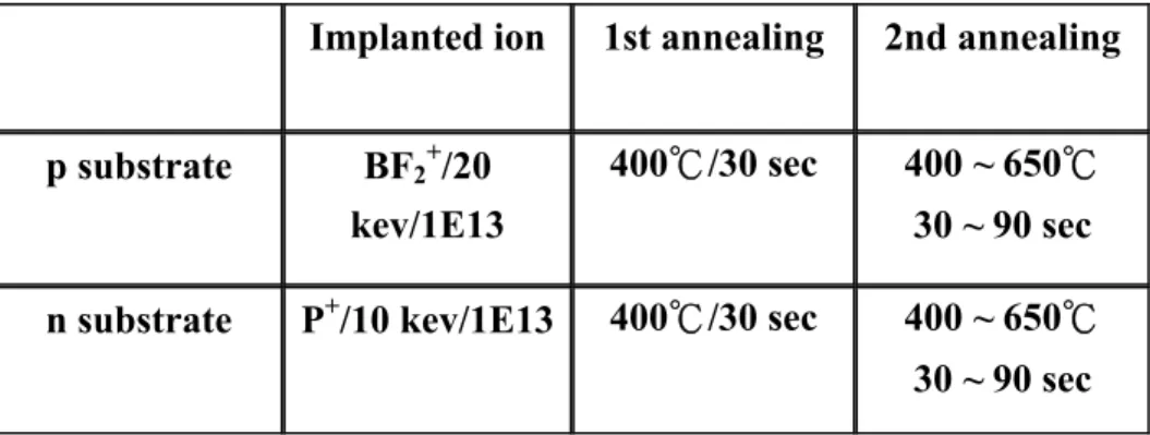
Implanted ion 1st annealing 2nd annealing p substrate BF2+/20
kev/1E13
400℃/30 sec 400 ~ 650℃ 30 ~ 90 sec n substrate P+/10 kev/1E13 400℃/30 sec 400 ~ 650℃
30 ~ 90 sec
(a) (b)
(c) (d)
Fig. 3-1 AFM image shows NiSi/Si interface morphology by 2nd RTP annealing (a) 400 ℃ (b) 500 ℃ (c) 600 ℃ (d) 700 ℃ for 30 sec.
Fig. 3-2 RMS value of the interface roughness versus temperature with / without 2nd RTP annealing.
400 450 500 550 600 650 700 0.8 0.9 1.0 1.1 1.2 1.3 1.4 1.5 1.6 1.7 1.8 1.9 2.0 R M S v a lue of ro ughne ss ( n m) Temperature (OC )
with 2nd 30 sec RTA w/o 2nd RTA
Fig. 3-3 SEM image shows NiSi formed by RTP annealing 400 ℃ for 30 sec.
(a)
(b)
Fig. 3-5 The ID-VD characteristic curves of the NiSi/Si junction diode
without 2nd RTA by (a) BF2+ implantation and (b) P+ implantation.
-2 -1 0 1 2 0.00 0.01 0.02 0.03 0.04 I D (mA) VD (Volts) w/o 2nd RTA -2 -1 0 1 2 -0.005 0.000 0.005 0.010 0.015 0.020 0.025 0.030 ID (mA) VD (Volts) w/o 2nd RTA
(a)
(b)
Fig. 3-6 The forward ID-VD characteristic curves of the NiSi/Si
junction diode with 2nd RTA 30 sec by (a) BF2+ implantation and (b)
P+ implantation. 0.0 0.5 1.0 1.5 2.0 0.0 0.5 1.0 1.5 2.0 I D (mA ) VD (Volts) w/o 2nd RTA w 2nd RTA 400 0C 30 sec w 2nd RTA 450 0C 30 sec w 2nd RTA 500 0C 30 sec w 2nd RTA 550 0C 30 sec w 2nd RTA 600 0C 30 sec w 2nd RTA 650 0C 30 sec 0.0 0.5 1.0 1.5 2.0 0.00 0.05 0.10 0.15 0.20 0.25 I D (mA ) VD (Volts) w/o 2nd RTA w 2nd RTA 400 0C 30 sec w 2nd RTA 450 0C 30 sec w 2nd RTA 500 0C 30 sec w 2nd RTA 550 0C 30 sec w 2nd RTA 600 0C 30 sec w 2nd RTA 650 0C 30 sec
(a)
(b)
Fig. 3-7 The ID-VD characteristic curves of the NiSi/Si junction diode
with 2nd RTA 30 sec by (a) BF2+ implantation and (b) P+
implantation. -2 -1 0 1 2 -2.0 -1.5 -1.0 -0.5 0.0 0.5 1.0 1.5 2.0 I D (mA) VD (Volts) w/o 2nd RTA w 2nd RTA 400 0C 30 sec w 2nd RTA 450 0C 30 sec w 2nd RTA 500 0C 30 sec w 2nd RTA 550 0C 30 sec w 2nd RTA 600 0C 30 sec w 2nd RTA 650 0C 30 sec -2 -1 0 1 2 -0.30 -0.25 -0.20 -0.15 -0.10 -0.05 0.00 0.05 0.10 0.15 0.20 0.25 I D (mA ) VD (Volts) w/o 2nd RTA w 2nd RTA 400 0C 30 sec w 2nd RTA 450 0C 30 sec w 2nd RTA 500 0C 30 sec w 2nd RTA 550 0C 30 sec w 2nd RTA 600 0C 30 sec w 2nd RTA 650 0C 30 sec
(a)
(b)
Fig. 3-8 The forward bias current density versus annealing temperature for the NiSi / Si junction diodes fabricated with (a) BF2+
and (b) P+ implantation at various annealing time.
400 450 500 550 600 650 0.01 0.1 1 10 100 1000 10000 For war d C u rr e nt D e ns it y ( A /c m 2 ) Temperature (OC ) Dose : 1E13 cm-2 Energy : 20 keV 30 sec anneal 60 sec anneal 90 sec anneal 400 450 500 550 600 650 1E-4 1E-3 0.01 0.1 1 10 100 1000 For w a rd C u rr e n t De nsity ( A /cm 2 ) Temperature (OC ) Dose : 1E13 cm-2 Energy : 10 keV 30 sec anneal 60 sec anneal 90 sec anneal
(a)
(b)
Fig. 3-9 The reverse bias current density versus annealing temperature for the NiSi / Si junction diodes fabricated with (a) BF2+
and (b) P+ implantation at various annealing time.
400 450 500 550 600 650 0.01 0.1 1 10 100 1000 10000 Reverse Cu rren t Densi ty (A/ c m 2 ) Temperature (OC ) Dose : 1E13 cm-2 Energy : 20 keV 30 sec anneal 60 sec anneal 90 sec anneal 400 450 500 550 600 650 1E-3 0.01 0.1 1 10 100 1000 10000 Re verse Cu rre n t Den s it y (A /cm 2 ) Temperature (OC ) Dose : 1E13 cm-2 Energy : 10 keV 30 sec anneal 60 sec anneal 90 sec anneal
Fig. 3-10 The capacitance-voltage characteristics of Schottky junction diodes implanted (a) BF2+ and (b) P+ without 2nd RTA.
-2 -1 0 1 2 0 500 1000 1500 Cap a ci tance (p F) VD (Volts) w/o 2nd RTA -2 -1 0 1 2 0 50 100 150 200 250 Ca pa cita nce (pF) VD (Volts) w/o 2nd RTA
(a)
(b)
Fig. 3-11 The doping concentration versus depth for the implanted (a) BF2+ and (b) P+ by annealing at various temperature.
0 2 4 6 8 10 12 14 1E12 1E13 1E14 1E15 1E16 1E17 1E18 1E19 1E20 1E21 Co n cen trati o n (cm -3 ) Depth ( µm) w/o 2nd RTA w 2nd RTA 400 0C w 2nd RTA 450 0C w 2nd RTA 500 0C w 2nd RTA 550 0C w 2nd RTA 600 0C w 2nd RTA 650 0C 0 2 4 6 8 1E12 1E13 1E14 1E15 1E16 1E17 1E18 1E19 1E20 1E21 1E22 1E23 C o nc e n tr a tion (c m -3 ) Depth ( µm) w/o 2nd RTA w 2nd RTA 400 0C w 2nd RTA 450 0C w 2nd RTA 500 0C w 2nd RTA 550 0C w 2nd RTA 600 0C w 2nd RTA 650 0C
(a)
(b)
Fig. 3-12 The Active charge versus anneals temperature for (a) Boron and (b) Phosphorous implant.
400 450 500 550 600 650 0.00E+000 2.00E+012 4.00E+012 6.00E+012 8.00E+012 1.00E+013 1.20E+013 Act ive d ch arg e (c o lu m e/ cm -2 ) Temperature (OC ) Boron 30 sec annealing dese : 1E13 cm-2 400 450 500 550 600 650 2.00E+012 4.00E+012 6.00E+012 8.00E+012 1.00E+013 Act ived ch a rg e ( co lu m e/ cm -2 ) Temperature (OC ) Phosphorous 30 sec annealing dese : 1E13 cm-2
簡歷 姓 名:孫 成 業 性 別:男 出生日期:民國 70 年 7 月 19 日 出 生 地:台灣省台北市 住 址:桃園縣八德市僑興新村 103 號 學 歷:國立高雄應用科技大學電子工程系 (民國 88 年 9 月~民國 93 年 6 月) 國立交通大學電子工程所 (民國 93 年 9 月~民國 95 年 9 月) 碩士論文:形成矽化鎳時在矽化鎳與矽接面處離子活化相關研究
Research of Dopant Activation at the Interface between Nickel Silicide and Silicon during Nickel Silicide Formation
![Fig. 3-4 Four basic transport process under forward bias. [1]](https://thumb-ap.123doks.com/thumbv2/9libinfo/8440312.181810/46.892.176.722.213.728/fig-basic-transport-process-forward-bias.webp)