國
立
交
通
大
學
光電工程研究所
碩
士
論
文
利用光激發-兆赫波探測研究飛秒雷射退火非晶矽
Optical-Pump-THz-Probe Studies of Femtosecond-Laser
Annealed Amorphous Silicon
研 究 生:莊君豪
指導教授:潘犀靈 教授
安惠榮 教授
利用光激發-兆赫波探測研究飛秒雷射退火非晶矽
Optical-Pump-THz-Probe Studies of Femtosecond-Laser
Annealed Amorphous Silicon
研 究 生:莊君豪
Student:Chun-Hao Chuang
指導教授:潘犀靈 教授
Advisors:Prof. Ci-Ling Pan
安惠榮 教授
Prof.
Hyeyoung
Ahn
國 立 交 通 大 學
光 電 工 程 研 究 所
碩 士 論 文
A Thesis
Submitted to Department of Photonics & Institute of Electro-Optic Engineering
College of Electrical Engineering National Chiao Tung University In partial Fulfillment of the Requirements
for the Degree of Master of Engineering
In
Electro-Optical Engineering
July 2007
Hsinchu, Taiwan, Republic of China
利用光激發-兆赫波探測研究飛秒雷射退火非晶矽
學生: 莊君豪
指導教授: 潘犀靈 教授
安惠榮 教授
國立交通大學光電工程研究所碩士班
摘
要
在本論文中,光激發-兆赫波探測技術被利用來研究複晶矽的光電特性
如載子回復生命期、載子漂移速度。複晶矽是利用鈦藍寶石超快雷射對非
晶矽進行雷射退火結晶而成。由於超短脈衝雷射導致材料的非線性吸收效
應在材料表面產生緻密的電漿,使得非晶矽發生非線性熔融。我們利用光
激發-兆赫波探測技術和兆赫時域光譜技術去研究複晶矽結構特性。
實驗上,我們利用雙指數函數去尋找適合由於光激發所引起的兆赫脈衝
振幅改變的鬆弛時間參數。對於具有較大晶粒(約 500 nm)和較小晶粒(約
50 nm) 的複晶矽而言,鬆弛時間分別是 32.69 皮秒和 24.43 皮秒。利用兆
赫時域光譜技術,對於不同晶粒大小的複晶矽而言,Drude模型能提供吻合
的趨勢線對於在兆赫波段下的導電率。同時藉由Drude模型得知,載子遷移
率分別是 175±19.4 cm
2/Vs和 94.5±20.2 cm
2/Vs對於較大晶粒(約 500 nm)
和較小晶粒(約 50 nm)。最後我們比較利用電性量測方式得到由複晶矽製成
的薄膜電晶體元件後的載子遷移率和利用Drude model得到的載子遷移率。
得知載子遷移率與複矽晶的晶粒大小呈現正相關的關係。
Optical-Pump-THz-Probe Studies of Femtosecond-Laser
Annealed Amorphous Silicon
Student:Chun-Hao
Chuang
Advisors: Dr. Ci-Ling Pan
Dr. Hyeyoung Ahn
Department of Photonics and Institute of Electro-Optic Engineering
National Chiao Tung University
ABSTRACT
We use the optical-pump–terahertz-probe technique (OPTP) to study relaxation dynamics of photo excited carriers in polycrystalline silicon. The polycrystalline silicon is prepared by femtosecond laser annealing (FLA) using near-infrared (λ = 800 nm) ultrafast Ti:Sapphire laser system. The intense laser pulses make the generation of dense photoexcited plasma in the irradiated materials due to nonlinear absorption, enabling nonlinear melting on silicon materials. We study the structural characteristics of recrystallized amorphous silicon by OPTP and THz-TDS system.
By using double exponential function to fit the pump-induced changes in transmission of the amplitude of the THz pulse, for large grain size (~500 nm) and small grain size (~50 nm), the relaxation time is 32.69 ps and 24.43 ps, respectively. We show that Drude model provides good fit to the transient terahertz conductivity in the two different grain sizes of polycrystalline silicon. The transient motilities of poly-Si for large grain size (~500 nm) and small grain size (~50 nm) are 175±19.4 cm2/Vs and 94.5±20.2 cm2/Vs, respectively. We also compare the mobility calculated by electrical characteristics measurement of poly-Si thin film transistor devices with the results calculated from OPTP measurement.
Acknowledgement (誌謝)
回首,兩年在風城的研究生活,是由涓涓不斷的努力與嘗試所匯成,
最後能夠順利地開花結果,首先要感謝的是我的指導教授潘犀靈教授與安
惠榮教授,在實驗方向與結果討論的指點,我從中獲益良多。在實驗過程
當中,感謝 Mika 學長願意耐心地跟我討論所遭遇的問題,使我能順利突破
瓶頸,再來要謝謝一起努力過來的伙伴,昀浦、彥毓、哲睿、韋文、宜貞,
在這兩年中,我們一同地歡笑與努力,將成為我值得回憶的時光,。感謝
Moya 學長、介瑋、孟桓、育賢、松輝在實驗和生活上的幫助與鼓勵,使我
在實驗室的生活更多彩多姿。
感謝父母對我的支持,始終對我懷抱著信心,總是讓我在通完電話後
又有足夠的動力去面對明天的挑戰,也謝謝雅琳、雅玟在我回家時,能與
你們聊聊學校裡的趣事,體會到親情的溫暖,最後謝謝翊甯,總是陪我在
實驗室待到很晚,有你的陪伴這兩年似乎不會那麼難熬。
走在苦澀的研究之路,有你們的陪伴和支持,是這無形的動力,驅使
我堅持到最後,願將最後果實的甜蜜,與你們共享。
君豪 2007/08/21
Contents Page
Abstract (Chinese)……….. i Abstract (English) ……….. ii Acknowledgement (誌謝)……….. iii Contents………... iv List of Figures………. vi List of Tables………... ix Chapter 1 Introduction……… 1Chapter 2 Generation and Detection of THz Radiation………... 5
2.1 THz Generation Mechanism from Semiconductor Surface………. 5
2.1.1 Optical Rectification……… 5
2.1.2 Surge Current………... 9
2.1.2.1 Surface Depletion Field……… 9
2.1.2.2 Photo-Dember Effect……… 11
2.2 Electro-Optical Crystal and Free Space Electro-Optic Sampling (FS-EOS)………... 13
2.2.1 Electro-Optical Crystal………. 13
2.2.2 Electro-Optic Sampling (FS-EOS)………... 18
Chapter 3 Experiment Setup and Method of Analysis……….. 20
3.1 Introduction of Femtosecond Laser System………. 20
3.2 The Terahertz Time-Domain Spectroscopy (THz-TDS)……….. 23
3.3 The Optical-Pump-Terahertz-Probe System (OPTP)………... 25
3.4 Extraction of Optical Constant for THz-TDS Experiment………... 28
3.5 Determination of Mobility and Conductivity from Drude Model……… 31
Chapter 4 Properties and Preparation of Low Temperature Poly-Silicon……….. 32
4.1 Introduction of Low Temperature Poly-Silicon………... 32
4.2.1 Sample Preparation……….. 36
4.2.2 Femtosecond Laser Annealing (FLA)……….. 37
4.2.3 The Laser Annealing Station……… 38
4.3 Characterization of Annealing Samples………... 39
Chapter 5
Results and Discussions………. 40
5.1 Free Space of THz Spectroscopy………. 40
5.2 Optical Pump Terahertz Probe Measurement………... 42
5.2.1 Amorphous Silicon and Single Crystal Silicon……….... 42
5.2.2 Polycrystalline Silicon……….. 43
5.3 THz-TDS measurement……… 46
5.3.1 Single Crystal Silicon………... 46
5.3.2 Polycrystalline Silicon……….. 48
5.3.3 Recovery Trend of Polycrystalline Silicon………... 51
5.4 Electrical Characteristics Measurement of Poly-Si TFT Devices……… 56
5.4.1 Fabrication of Poly-Si TFT Devices……….... 56
5.4.2 Determination of Field –Effect Mobility………. 57
5.4.3 Electrical Characteristics Comparisons between Poly-Si TFTs and THz-TDS System………. 58
Chapter 6 Conclusions and Future Works………. 60
List of Figures Page
Fig. 1-1 Electromagnetic spectrum... 1 Fig. 2-1 The optical beam refraction and THz beam refraction in the semiconductor
surface………... 8
Fig. 2-2 Band picture and the schematic flow of drift current in (a) for n-type and (b)
for p-type……….. 10
Fig. 2-3 The schematic flow of diffusion current near the surface of semiconductor which is induced by photoexcited carriers………... 12 Fig. 2-4 (a) Schematic ZnTe crystal and (b) the refractive index in Z” and Y” axis
are changed by THz pulse……… 17
Fig. 2-5 The schematic picture of how to measure THz signal………. 19 Fig. 3-1 Femtosecond laser system includes Tsunami, Spitfire and two pump laser
(Millennia V and Empower)………. 21
Fig. 3-2 The chirped amplification process……… 22 Fig. 3-3 The scheme of the terahertz pulse setup. BS: beam splitter; B: polyethylene
visible beam block; F: blue filter; WP: Wollaston prism; P: pellicle………... 24 Fig. 3-4 The scheme of the optical pump terahertz probe setup. BS: beam splitter; B:
polyethylene visible beam block; F: blue filter; WP: Wollaston prism; P:
pellicle……….. 26
Fig. 3-5 The scheme of poly-Si and sample mount with 2mm-diameter aperture……. 27 Fig. 3-6 The schematic sample between pump and unpump. n1, n2, n3 is the
refractive indices. E0(ω) is the incident THz field. Eref(ω) and Efilm(ω) are
the reference (without pump) and sample (with pump)………... 28 Fig. 4-1 The crystal structure and electrical characteristics performance comparison
between the silicon thin films……….. 33 Fig. 4-2 Concepts of circuit integration. The comparison of a-Si TFT-LCD, poly-Si
TFT-LCD and poly-Si TFT-LCD system on panel. PCB means printed
circuit board……….. 34
Fig. 4-3 Schematic description of LPCVD device [42]………. 36 Fig. 4-4 Schematic diagram of femtosecond laser annealing experiment setup……… 38 Fig. 4-5 SEM images of FLA poly-silicon samples after Secco etching for scanned
FLA (a) the average grain size is about 500nm, (b) the average grain size is
about 50nm………... 39
Fig. 5-1 (a) THz electric field profile in the time domain. (b) Amplitude spectrum
versus frequency of the THz pulse in (a)……….. 41 Fig. 5-2 (a) Differential transmission curves for 400nm pump at a fluence of 424
μJ/cm2
curves at various 400nm pump fluence for amorphous silicon……… 42 Fig. 5-3 Differential transmission curves of single crystal silicon for 400nm pump at
a fluence of 636 μJ/cm2……….. 43
Fig. 5-4 Differential transmission of the peak of the THz pulse for sample A and
sample B………... 45
Fig. 5-5 Light absorption in silicon as a function of depth and wavelength[46]……... 45 Fig. 5-6 (a) Amplitude spectrum of THz pulse. Measured frequency-dependent
complex conductivity and refractive index (b) Re[σ ] and Im[σ ], (c) Re[refractive index], (d) Im[refractive index] for single crystal silicon film at 100ps after excitation (636 μ J/cm2). Solid lines are fits to the Drude
model with parameters give in Table 5-2………. 47 Fig. 5-7 (a) Amplitude spectrum of THz pulse. Measured frequency-dependent
complex conductivity and refractive index (b) Re[σ ] and Im[σ ], (c) Re[refractive index], (d) Im[refractive index] for Sample A at 10ps after excitation (636 μ J/cm2). Solid lines are fits to the Drude model with
parameters give in Table 5-3……… 49
Fig. 5-8 (a) Amplitude spectrum of THz pulse. Measured frequency-dependent complex conductivity and refractive index (b) Re[σ ] and Im[σ ], (c) Re[refractive index], (d) Im[refractive index] for Sample B at 10ps after excitation (636 μ J/cm2). Solid lines are fits to the Drude model with
parameters give in Table 5-3……… 50
Fig. 5-9 (a) Amplitude spectrum of THz pulse. Measured frequency dependent complex conductivity and refractive index (b) Re[σ ] and Im[σ ], (c) Re[refractive index], (d) Im[refractive index] for Sample A at zero point after excitation (636 μ J/cm2). Solid lines are fits to the Drude model with
parameters give in Table 5-4……… 52
Fig. 5-10 (a) Amplitude spectrum of THz pulse. Measured frequency-dependent complex conductivity and refractive index (b) Re[σ ] and Im[σ ], (c) Re[refractive index], (d) Im[refractive index] for Sample A at 100ps after excitation (636 μ J/cm2). Solid lines are fits to the Drude model with
parameters give in Table 5-4……… 53
Fig. 5-11 (a) Amplitude spectrum of THz pulse. Measured frequency-dependent complex conductivity and refractive index (b) Re[σ ] and Im[σ ], (c) Re[refractive index], (d) Im[refractive index] for Sample A at 150ps after excitation (636 μ J/cm2). Solid lines are fits to the Drude model with
parameters give in Table 5-4……… 54
Fig. 5-12 The mobility and carrier concentration for sample A at different time delay
of optical pump beam………... 55
Fig. 5-14 Field effect mobilities for poly-Si TFTs annealed by FLA with different
List of Tables Page
Table. 3-1 Properties of Tsunami laser………. 21 Table. 3-2 Properties of Ti:Sapphire regenerative amplifier……… 22 Table. 5-1 Parameters for double exponential fits in Fig. 5-4……….. 45 Table. 5-2 Parameters for Drude model fitting in Fig. 5-6. First term of Bulk-Si is
measured by Hall measurement……….. 47
Table. 5-3 Parameters for Drude model fitting in Fig. 5-7 and Fig. 5-8………... 50 Table. 5-4 Parameters for Drude model fitting in Fig. 5-9. Fig. 5-7, Fig. 5-10 and
Chapter 1
Introduction
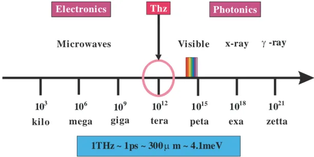
Past twenty years have observed a significant development of ultrafast terahertz (THz) technique. Opening of the THz era has made significant contribution not only to ultrafast phenomena, but to a wide variety of applications, including ultrahigh speed optoelectronics, tomographic imaging in biomedical fields. The THz radiation is roughly defined by the frequency range of 0.1 to 10 THz as shown in Fig. 1-1, which are between microwaves and visible light. These THz wave corresponds to the wavelengths of 0.003 to 1 mm, so THz waves are also called sub-millimeter wave.
At lower frequencies compared to THz wave, microwaves can be easily generated by “electronic” devices, such as a simple dipole antenna. At higher frequencies, visible light can be generated by “optical” devices, such as a semiconductor laser diode, in which electrons jump across the energy band gap and then emit light. Until 1980’s, the spectral range of THz has been inaccessible in both electronic and optical methods. Until then, Fourier transform spectroscopy is perhaps the most common technique to study sub-THz phenomena.
103 106 109 1012 1015 1018 1021 kilo mega giga tera peta exa zetta
Visible x-ray Microwaves Photonics Electronics γ -ray Thz Frequency (Hz) 1THz ~ 1ps ~ 300μ m ~ 4.1meV
The appearance of ultrashort pulse laser of ~100 ps pulse duration made it possible to generate THz waves covering the whole THz spectral range. In 1981, Mourou and Auston first demonstrated generation and detection of pulsed THz radiation by a photoconducting switch with advantages of time resolution of picosecond and high sensitivity enhanced by phase-lock technique [1, 2]. In 1988, Grischkowsky used the photoconductor dipole antenna as the THz sensor, furthering the spectrum into the order of terahertz frequency [3]. Afterward a variety of antennas was appeared, like typical dipole antenna, large aperture photoconductor dipole antenna [4] and also another method using semiconductor surface electric field [5] to generate THz pulses by the ultrashort pulse laser. In 1996, X. C. Zhang et al. developed free-space electro-optic sampling (FS-EOS) technique to enhance signal to noise ratio (S/N ratio) up to 105 and to achieve much large dynamic range [6].
THz wave has an infinite potential in application of science. In the bioscience, the photo energy of THz is much smaller than the traditional X-Ray and the pathological changes will not be induced by THz wave in human body. Since different tissues of body have different sensitivity for THz waves, more detailed information can be obtained through the tomographic THz imaging. Photon energy of THz wave is about 4 meV for 1 THz, which approximately equals to the binding energy of the excitons in many semiconductors. Most of all, recently developed THz waves possess ultrashort duration with broad bandwidth and provide both high sensitivity and time-resolved phase information. These advantages can be used in a number of applications, such as the study of carrier dynamics of condensed matters with high temporal and spectral resolutions.
Recently, the spectroscopic technique using pulsed THz radiation, called ”terahertz time-domain spectroscopy (THz-TDS)”, has been developed, by taking advantage of short pulses of broadband THz radiation. THz-TDS has the time resolution of sub-picosecond level and the spectral resolution of 50 GHz. And THz-TDS is a non-destructive method to the
carrier concentration and mobility of doped semiconductotrs. Many researches have been performed on a variety of gases, liquids, dielectric materials and semiconductors by THz-TDS. For example, in 1990, D. Grischkowsky et al. studied the THz-TDS with the dielectric materials, such as quartz and sapphire, and semiconductors, like silicon and GaAs. They discovered different carrier concentrations affect the absorption characteristics of the samples in the THz frequency range. The Drude Model could be used to link the frequency-dependent dielectric response to the material free-carrier dynamics properties [7].
Nowadays, with requesting of the decreased size and faster efficiency of devices, it is very important to understand the transient phenomena of the materials. As a result of the advancement of laser technology, laser pulse duration can be as short as 10-15 second. Optical
measurement can achieve higher time resolution and broader frequency domain than the electric measurement. Spectroscopic study with optical-pump THz-probe system can provide additional information of materials. In this time-resolved pump-probe technique, the dynamic far-infrared optical properties of the photoexcited materials can be studied.
Hydrogenated amorphous silicon (a-Si:H) is used extensively in Thin Film Transistors (TFTs) for Flat Panel Displays (FPDs) and large area imagers, and it is also a promising photovoltaic material. The a-Si:H TFTs have low off-current and sufficient on-current for most applications. But, a-Si:H has poor carrier mobility. The poor mobility will result in the limitation on the pixel sizes for display and other imaging application. Therefore, poly-Si with higher mobility up to 300cm2/Vs has been suggested as an alternative of a-Si:H. Higher performance poly-Si device has been applied in many applications, like flat panel displays.
In order to realize such system, System on plane (SOP), we introduced the low temperature polycrystalline silicon (LTPS). Low-thermal-budget techniques, such as plasma-assisted hydrogen [8], metal [9], and laser-induced crystallization [10-14]are
employed to LTPS for the region of channel. Particularly, excimer laser annealing results in high-quality polycrystalline silicon (poly-Si) due to the efficient absorption of the ultraviolet (UV) laser radiation [12-14].
In our experiment, we used the femtosecond (fs) laser pulses to annealed the a-Si:H. Unlike the thermal annealing using continuous-wave [15] and long pulsed lasers (tens of nanosecond range), in fs-laser annealing, nonlinear photon absorption and non-equilibrium thermodynamics are expected to dominate [16-21]. The nonlinear process provides a precise and low fluence associated with femtosecond laser ablation [18-21].
In this thesis, our samples are the poly-Si annealed by a near-infrared (λ = 800 nm) femtosecond laser with 50fs pulse duration. The determination of the grain size of annealed poly-Si is an important task for its application in TFT fabrication. Typically, Hall measurement could not measure the electrical constant due to the similar characteristic between poly-Si and silicon substrate. SEM images of the annealed samples identify the grain size, but this method has the intrinsic restrictions, such as the limited imaging area and destructive sample preparation procedure. In this thesis, we introduced optical pump-THz probe method and THz-TDS system to directly identify the annealing quality of poly-Si in a large area without any preparation process. We also use the terahertz time-domain spectroscopy (THz-TDS) to study the ultrafast carrier dynamics in the poly-Si.
In chapter 2 of this thesis, we mainly describe the theories of generation and detection of THz field. In chapter 3, the femtosecond laser system, the experimental setup of THz system and the method of analysis will be introduced. In chapter 4, we describe the preparation of the sample. In chapter 5, we show the experimental results and discussions. At last, we make conclusions in chapter 6.
Chapter 2 Generation and Detection of THz Radiation
We separate this chapter into two sections. In section 2.1, we introduce the THz generation mechanism from semiconductor surfaces. In section 2.2, electro-optic sampling technique (FS-EOS) is given in detail.
2.1 THz Generation Mechanism from Semiconductor Surface
In 1990, Zhang et al [22] found THz radiation can be generated by illuminating semiconductor surface with intense femtosecond laser pulses. Generally, THz radiation from photoexcited semiconductor surface is weaker than other THz radiation sources, such as photoconductive antennas and phase-matched nonlinear crystals. Several methods have been proposed to enhance the THz emission efficiency from the semiconductors, such as applying the external magnetic field on the surface of InAs [23, 24]. A number of different mechanisms have been proposed to generate THz radiation, including photocarrier acceleration in photoconducting antennas, the second-order nonlinear optical processes in semiconductors, and the surge current normal to the surface [22, 25]. Photoconduction and optical rectification are two of the most common approaches for generating broadband pulsed THz waves and will be discussed in the following sections.
2.1.1 Optical Rectification
THz emission from nonlinear optical process is explained as the optical rectification of ultrashort laser pulses, which creates a transient polarization on the semiconductor surface. This process is described in the frequency domain as the difference-frequency mixing (DFM) between spectrum components of the femtosecond laser pulse in the semiconductors. The THz generation due to the optical rectification,ETHz(t), is proportional to the second order
nonlinear polarization (in the near field), which is described in the following equation: Ω Ω = +∞ −Ω ∞ −
∫
d e P t P ( ) i t 2 1 ) ( (2) π , (1)∑
+∞∫
∞ − + Ω = ⋅ − = Ω = Ω k j ijk j k i E E d P , 1 2 1 2 2 2 ) 2 ( 0 ) 2 ( ( ) ε χ ( ω ω ) (ω ω ) (ω ) ω , (2)where (2) is the second-order nonlinear susceptibility tensor for a difference frequency,
ijk χ 2 1 ω ω − =
Ω , and Ej(ω1)Ek(ω2) is the amplitude spectral component of the pump laser at frequency ω1,ω2 in the j, k direction. Here, i, j and k are the dummy indices for x-, y- and z-directions in the crystallographic axis system. The integral is extended to the negative frequency by using the definition, E(−ω)=E∗(ω).
In the far field, the THz field amplitude, , is proportional to the projection of the second time derivative of the nonlinear polarization to the polarization direction of detection, (a unit direction normal to the observed direction). At the observed direction, the THz field amplitude in the far field can be explained as:
far THz E e 2 2 ( ) ) ( t t P e E e t Efar THz THz ∂ ∂ ⋅ ∝ ⋅ = , (3)
The spectral amplitude, far(Ω), at the frequency
THz
E Ω can be expressed as:
) ( ) (Ω ∝Ω2e⋅P Ω Efar THz . (4)
The clear evidence for the contribution of the optical rectification is the strong dependent of the emitted THz radiation intensity on the crystal orientation to the pump laser polarization. By rotating the sample about the normal direction of the surface, the relative contribution of the azimuthal angle dependence of DFG component to the total THz emission can be estimated.
laboratory frame. The polarization which induced by the optical rectification in the semiconductor for (111) and (100) surface can be expressed as (5) and (6), respectively [26]
⎟ ⎟ ⎟ ⎠ ⎞ ⎜ ⎜ ⎜ ⎝ ⎛ Ω Ω Ω = ) ( ) ( ) ( z y x P P P P . ⎟⎟ ⎟ ⎟ ⎟ ⎟ ⎟ ⎠ ⎞ ⎜⎜ ⎜ ⎜ ⎜ ⎜ ⎜ ⎝ ⎛ − + − Ω = θ φ φ φ θ φ φ φ ε 3 sin cos 6 2 sin cos 6 2 3 cos cos 6 2 sin 6 2 cos 3 1 ) ( 2 2 2 2 2 2 14 0d E , (5) ⎟ ⎟ ⎟ ⎠ ⎞ ⎜ ⎜ ⎜ ⎝ ⎛ Ω Ω Ω = ) ( ) ( ) ( z y x P P P P . ⎟ ⎟ ⎟ ⎠ ⎞ ⎜ ⎜ ⎜ ⎝ ⎛ Ω = θ φ θ φ θ φ ε 2 cos 2 sin 2 sin 2 sin 2 sin cos ) ( 2 2 2 14 0d E , (6) 2 2 2 1 2 2 2 1 2 ) ( ) ( ) ( ) ( ) ( ω ω ω ω ω ω ω ω d E E d E E E ∗ ∞ ∞ − ∞ ∞ −
∫
∫
− Ω = = + Ω = = Ω . (7)Here, φ is the angle between the surface normal and the pump-laser beam refracted inside the sample, θ is the azimuthal angle of the sample orientation around the x-axis,
) ( i
E ω is the amplitude component of the pump laser for frequency ωi, and
is the nonlinear susceptibility coefficient for the difference frequency, , in the contracted notation, and 2 / ) 2 ( 14 14 =χ d Ω ) (Ω
E is the autocorrelation function of E(ω).
Using (3) and considering the refraction at the interface between the semiconductor/air interfaces in Fig. 2-1, the p-polarized THz field amplitude observed in the direction of optical
reflection is given by the following equation: ) , , )( 0 , cos , sin ( THz THz x y z THz eP P P P E ∝ = − φ φ Thz y THz x P P sinφ + cosφ − = (8)
where φTHz is the refraction angle of THz radiation inside the semiconductor.
Fig.2-1. the optical beam
refraction and THz beam refraction in the semiconductor surface. [27]
The refraction angles for the optical and THz beams are determined by the generalized Snell’s law as: THz THz opt n n sinφ sinφ 45 sin o = = (9)
where and is the refractive index for the pump laser and THz radiation in the
semiconductor, respectively. For the pump-laser wavelength of 800 nm, φ is and for InAs and InSb, respectively. For THz radiation,
opt n nTHz o 9 . 10 9.0o THz φ is estimated to be and
for InAs and InSb, respectively. Using these values, the azimuthal-angle dependence of the radiation amplitude due to the optical rectification can be written as follows:
o 9 . 10 0 5 . 21 ) 103 . 0 3 (cos 093 . 1 14 − ∝ d θ
ETHz for (111)-InAs (10a)
θ 2 sin 1823 . 0 d14 ETHz ∝ for (100)-InAs (10b) θ 2 sin 069 . 0 d14 ETHz ∝− for (100)-InSb (10c)
with a small DC offset for (111)-oriented crystals, and sin 2θ for (100)-oriented crystals. The azimuthal angle dependences for the other (100)-oriented samples were as weak as that observed for the n-InSb sample and InAs sample.
From the results of the azimuthal-angle dependence, it is concluded that the nonlinear contribution to THz radiation is finite but not very significant for the (100)-oriented zincblende-type semiconductor surfaces, while it can be very significant for the (111)-oriented ones.
2.1.2 Surge Current Contribution
2.1.2.1 Surface Depletion Field
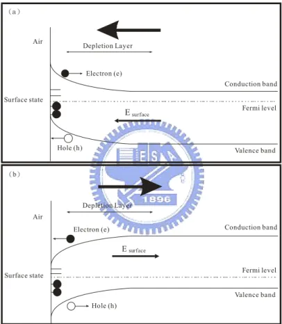
In semiconductors with a wide bandgap, such as GaAs (Eg = 1.43 eV) or InP (Eg = 1.34
eV), the surface bands of a semiconductor lie within its energy bandgap, and thus Fermi-level pinning occurs, leading to band bending and formation of a depletion region, where the surface built-in field exists [28]. When laser beam excites the semiconductor surface, the electrons and holes are accelerated in opposite directions under the surface-depletion field, then a surge current are formed in the direction normal to the surface. The direction and magnitude of the surface depletion field depend on the dopants, impurity species and the position of the surface states relative to the bulk Fermi level. Generally, the energy band of n-type semiconductors is bent upward (Fig. 2-2(a)) and the energy band will bend downward for p-type semiconductors (Fig. 2-2(b)). The field built in surface in p-type semiconductors drives the photogenerated carriers, which is the transient surge current. In the n-type semiconductor, the transient surge current is driven in opposite direction compared to p-type semiconductor as shown in Fig. 2-2(a). In the far-field approximation, the emitted THz-radiation-field amplitude, ETHz(t), is proportional to the time derivative of the surge
t t J t ETHz ∂ ∂ ∝ ( ) ) ( . (11)
The unambiguous evidence for distinguishing the main mechanism of THz emission from semiconductor surface is the polarity of the THz waveform between the n-type and p-type semiconductor. When the surface depletion field is the dominant mechanism for the surge current, the polarity of the THz waveform is opposite between the n-type and p-type semiconductors. Depletion Layer Conduction band Valence band Fermi level Hole (h) Air Surface state Electron (e) Esurface ( )a Electron (e) Depletion Layer Hole (h) Conduction band Valence band Fermi level Air Surface state Esurface ( )b
Fig. 2-2. Band picture and the schematic flow of drift current in (a) for n-type and (b) for p-type.
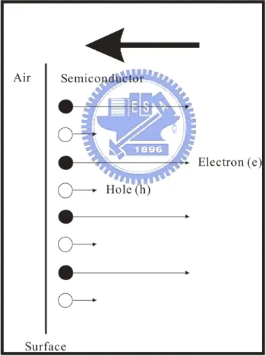
2.1.2.2 Photo-Dember Effect
InAs and InSb are very interesting materials because of their high electron mobilities: ≈ 30000 cm2/Vs for InAs and ≈ 76000 cm2/Vs for InSb, respectively. Recently, InAs attracts much attention as an efficient THz emitter since a significant enhancement of THz emission from InAs has been observed under magnetic fields [29]. The effect of surface depletion field is not so large for the narrow-bandgap semiconductors because of their small bandgap energies. The absorption depth of a narrow bandgap semiconductor surface photoexcited by near infrared light (h =1.5 eV) is very thin ( 100ν ≈ nm) [30], and the excess energy of the photoexcited carrier is very large. THz generation from the narrow-bandgap semiconductors is mainly due to the Photo-Dember effect, which is known to generate current or voltage in semiconductors attributed to the difference of the electron and hole diffusion velocities.
The diffusion current due to the Photo-Dember effect after photoexcitation near a semiconductor surface is illustrated in Fig. 2-3. Because the electron mobility is always larger than the hole mobility, the direction of diffusion current induced by the Photo-Dember effect is in the same way for each kind of semiconductor and irrespective of the doping type (n or p). Therefore, the THz waveform emitted from the surface surge current due to the Photo-Dember effect will show the same polarity for n-type and p-type semiconductors.
The diffusive currents of the electrons ( ) and holes ( ) are, respectively, described by the following equations [31],
n J Jp x n eD Jn e ∂ Δ ∂ − ∝ , (12) x p eD Jp h ∂ Δ ∂ ∝ , (13)
where is the electron unit charge, e Δ and n Δp are the density of photocreated electrons and holes, and are the diffusion coefficient of electrons and holes, respectively. The diffusion coefficient is defined by the Einstein relation,
e
D Dh
Boltzman constant, T is the temperature of the corresponding carrier, and μ is the mobility of electrons or holes. The THz radiation from the Dember current Jdif =Jn +Jpis proportional to the difference in the mobility for the electrons and holes, and the gradient of the carrier density.
Narrow bandgap semiconductors have the ability to create a large Photo-Dember field due to the large electron mobility and large excess carrier energies. Moreover, the Photo-Dember field in the narrow bandgap semiconductors is further enhanced by the small absorption depth. Electron (e) Hole (h) Semiconductor Air Surface
Fig. 2-3. The schematic flow of diffusion current near the surface of semiconductor which is induced by photoexcited carriers.
2.2 Electro-Optical Crystal and Free Space Electro-Optic Sampling (FS-EOS)
Under the external field, the refractive index of a certain material can be changed with the field intensity. This effect is called Electro-Optical Effect. In 1996, X. C. Zhang found that THz pulse can be detected by electro-optic sampling methods [6]. The THz electric field modulates the birefringence of the EO crystals and then modulates the polarization ellipticity of the optical probe beam passing through the crystal with the time delay. The ellipticity modulation of the optical beam can then be analyzed to provide information of the amplitude and phase of the applied electric field.
2.2.1 Electro-Optical Crystal
Without external electric field, the spatial distribution of crystal refractive index can be expressed with the index ellipsoid:
1 =
∑
ij ij i j χ χ η , (14)where η is the dielectric impermeability tensor, ij . Without external electric field, crystal’s dielectric impermeability tensor is . With the external electric field, crystal’s dielectric impermeability become
2 0 / ij 1/n ij =ε ε = η 2 0 0 1 n/ ij = η ij
η , where η can be expanded with ij
electric field as:
∑
+∑
+ + = k kl l k ijkl k ijk ij ij(E) η0 r E S E E ... η , i, j, k, l=1, 2, 3 (15)∑
+∑
= − = Δ k ijk k kl ijkl k l ij ij ij E r E S E E 0 ) ( η η η . (16) ij ηΔ is the variation of the refractive index, which is expressed with dielectric
impermeability, induced by electric field. In equation (16), the variation of refractive index induced by the second item is called Pockels effect or linear electro-optical effect. The refractive index is proportional to the electric field intensity. rijk is the Pockels coefficient.
The third term is the Kerr effect, Sijkl is Kerr coefficient.
In our experiment, we use the linear electro-optical effect in the ZnTe crystal to detect THz signal. The effect induced by electric field is expressed as:
∑
= Δ k ijk k ij r E η . (17)In general, it needs to be represented by 27 sections. Owing to the characterization of
ji ij η
η = , the subindex ij can be represented by l.
ij = 11, 22, 33, (23, 32), (13, 31), (12, 21) l= 1, 2, 3, 4, 5, 6. ⎥ ⎥ ⎥ ⎥ ⎥ ⎥ ⎥ ⎥ ⎦ ⎤ ⎢ ⎢ ⎢ ⎢ ⎢ ⎢ ⎢ ⎢ ⎣ ⎡ = 63 62 61 53 52 51 43 42 41 33 32 31 23 22 21 13 12 11 r r r r r r r r r r r r r r r r r r rijk . (18)
Because ZnTe is high symmetric cubic 43m structure (nx =ny =nz), the Pockels coefficient can represent as:
⎥ ⎥ ⎥ ⎥ ⎥ ⎥ ⎥ ⎥ ⎦ ⎤ ⎢ ⎢ ⎢ ⎢ ⎢ ⎢ ⎢ ⎢ ⎣ ⎡ = 41 41 41 0 0 0 0 0 0 0 0 0 0 0 0 0 0 0 r r r rijk . (19)
The index ellipsoid can be rewritten as:
1 2 2 2 41 41 41 2 0 2 2 2 = + + + + + xy E r xz E r yz E r n z y x z y x , (20)
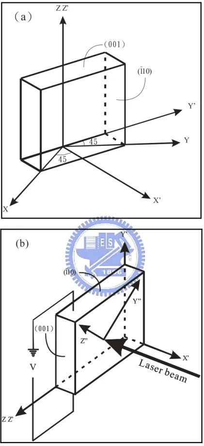
Suppose the external electric field is normal to the (110) plane and has no electric field in z direction. The schematic of the ZnTe crystal is shown in Fig. 2-4(a). The equation (20) can be
rewrite withEx = −E/ 2 andEy = −E/ 2. 2 2 2 41 2 0 2 ( ) x y z r E zx yz n + + + − 1 = . (21) Letˆ
(
ˆ' ˆ')
/ 2 y x x= − , ˆ(
ˆ' ˆ')
/ 2 y xy= + , zˆ z= , it make the electric field become ˆ' E=Eˆy'.
The equation (21) can simplify as:
'2 '2 '2 ' ' 41 2 0 2 x y z r Ey z n + + + 1 = . (22)
To make it more simply, we transform the coordinates again. Letxˆ"=xˆ', yˆ" =
(
yˆ'−zˆ')
/ 2,(
ˆ ˆ)
/ 2ˆ" y' z'
z = + , the equation (22) can be write as:
"2 "2 "2 41 41 2 2 2 0 0 0 1 1 ( ) ( ) x r E y r E z n + n − + n + = 1. (23) Let n , x" ny" , nz" is the refractive index in new axis direction and
2 0 41 z 1 n r E << in approximation. " o x n =n . (24) 1 2 3 " 2 41 1 1 2 y o o n r E n n n − ⎛ ⎞ =⎜ − ⎟ ≈ + ⎝ ⎠ or E . (25) 41 1 2 3 " 2 41 1 2 z o o n r E n n n − ⎛ ⎞ =⎜ + ⎟ ≈ − ⎝ ⎠ 41 1 or E . (26)
With external electric field, the refractive index increase 3 41
1
2n r Eo compared with refractive index without external electric field in direction. In the direction, the refractive index
decrease " ˆy ˆz" 3 41 1
2n r Eo compared with refractive index without external electric field. When light of linear polarization vertically incident the (110) plane of the ZnTe crystal, light polarized direction is normal to the (110) plane, the light of linear polarization will separate into two
light which polarized in and direction. Owing to the refractive index is different in and direction, the mutual phase delay is:
" ˆy ˆz" " ˆy ˆz" V r n d L E r Ln L n ny z o o3 41 41 3 2 2 ) ( 2 " " λ π λ π λ π − = = = Γ , (27)
where L is the thickness of ZnTe, d is the length of ZnTe in direction, V is the voltage we apply on ZnTe in direction. Fig. 2-4(b) show the change of refractive index in y” and z” axis when we apply a voltage on ZnTe. We define the voltage is half-wave voltage which make the passed light have phase different
' ˆy ' ˆy π V
π. It means Vπ have to satisfy below equation.
π λ π π = = Γ n r V d L o 41 3 2 . (28) 41 3 41 3 2 2 r Ln d r n d L V o o λ π λ π π =Γ= = . (29) π π V V = Γ . (30)
According to equation (27), the ZnTe crystal represent a wave plate which phase delay can be tuned by the electric field intensity.
(001) 45 45 X X’ Y Y’ Z Z’ (110)
( )
a
Y’ Z Z’ X’ Y” Z”Laser b
eam
V (110) (001) Y’ Z Z’ X’ Y” Z”Laser b
eam
V (110) (001)(b)
Fig. 2-4. (a) Schematic ZnTe crystal and (b) the refractive index in Z” and Y” axis are
2.2.2 Electro-Optic Sampling (FS-EOS)
We consider the ZnTe crystal as a wave plate and then the Jones matrix of the phase delay is represented as:
⎥ ⎥ ⎥ ⎦ ⎤ ⎢ ⎢ ⎢ ⎣ ⎡ Γ Γ − Γ − Γ = 2 cos 2 sin 2 sin 2 cos i i W . (31)
By using Jones matrix operation, the electric field intensity of y-axis polarization is represented as:
[
]
2 sin 1 0 2 cos 2 sin 2 sin 2 cos 0 1 ⎥=− Γ ⎦ ⎤ ⎢ ⎣ ⎡ ⎥ ⎥ ⎥ ⎦ ⎤ ⎢ ⎢ ⎢ ⎣ ⎡ Γ Γ − Γ − Γ = i i i Eout , (32) ⎟⎟ ⎠ ⎞ ⎜⎜ ⎝ ⎛ = = π π V V E Iout out 2 sin2 2 . (33)Equation (33) is the relation between the intensity of passed light and the applied voltage. In
order to make the relationship more linear dependence, the applied voltage 2
π
V
is needed by
put a quarter-wave plate after ZnTe crystal. This arrangement also agrees with the electric field intensity of z-axis polarization after ZnTe crystal. The relation between the electric field intensity of z-axis polarization is represented as:
[
]
2 cos 0 1 2 cos 2 sin 2 sin 2 cos 0 1 ⎥= Γ ⎦ ⎤ ⎢ ⎣ ⎡ ⎥ ⎥ ⎥ ⎦ ⎤ ⎢ ⎢ ⎢ ⎣ ⎡ Γ Γ − Γ − Γ = i i Eout , (34) ⎟⎟ ⎠ ⎞ ⎜⎜ ⎝ ⎛ = = π π V V E Iout out 2 cos2 2 . (35)The output of equation (34) has inverse phase. These two beams finally are received by a balance detector. The output of balance detector is the twice the electric field of eqs (32) and (34), and then the THz waveform can be detected.
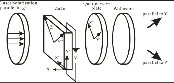
Wollaston Y’ Z” Y” Z’ X’ Z” Y” Y’ Z’ V
ZnTe Quarter wave plate
Laser polarization parallel to
parellel to
parellel to
Z’
Chapter 3 Experiment Setup and Method of Analysis
In chapter 3, we briefly describe our femtosecond laser system. The experimental setup of THz-TDS system and OPTP system will be introduced in section 3.2 and section 3.3, respectively. In section 3.4, we introduce the extraction method of optical constant for THz-TDS experiment. Finally, the determination of mobility and conductivity from Drude model are represented.
3.1 Introduction of Femtosecond Laser System
The invention of the laser in 1960 stimulated the development of optical physics and gave rise to many rising research fields. One of these rising research fields was ultrafast optics, which was rised and developed in mid-1960s with the production of nanosecond (10-9 s) pulses by the first mode-locked laser. Nowadays, a lot of progresses of ultrafast optics lead to some practical laser which can produce pulses on femtosecond (10-15 s) time scale. In this section, our femtosecond laser system will be briefly introduced.
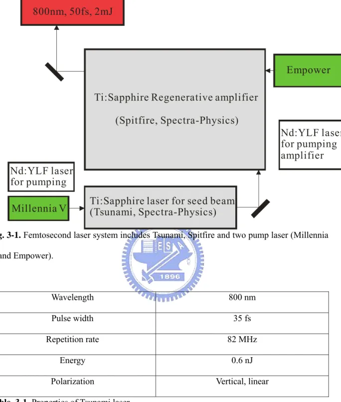
Our femtosecond later system is shown in Fig. 3-1. We use the Ti:Sapphire laser as the seeding laser which is then directed into the Ti:Sapphire regenerative amplifier (Spitfire, Spectra-Physics) for amplification.
The pump laser of Spectra Physics Tsunami laser is a 5W frequency doubled diode-pumped Nd:YLF laser (Millennia V, Spectra-Physics) with a wavelength λ=532 nm. The Ti:Sapphire laser provides an output trace of intense 35fs pulses with wavelengths ranging from 750nm to 850nm. The pulse repetition rate is ~82 MHz and the output power can up to 0.5W. The properties of the Ti:Sapphire laser is shown in Table. 3-1.
Ti:Sapphire Regenerative amplifier
(Spitfire, Spectra-Physics)
Ti:Sapphire laser for seed beam
(Tsunami, Spectra-Physics)
Millennia V
Empower
800nm, 50fs, 2mJ
Nd:YLF laser
for pumping
amplifier
Nd:YLF laser
for pumping
Fig. 3-1. Femtosecond laser system includes Tsunami, Spitfire and two pump laser (Millennia
V and Empower).
Wavelength 800 nm
Pulse width 35 fs
Repetition rate 82 MHz
Energy 0.6 nJ
Polarization Vertical, linear
Table. 3-1. Properties of Tsunami laser
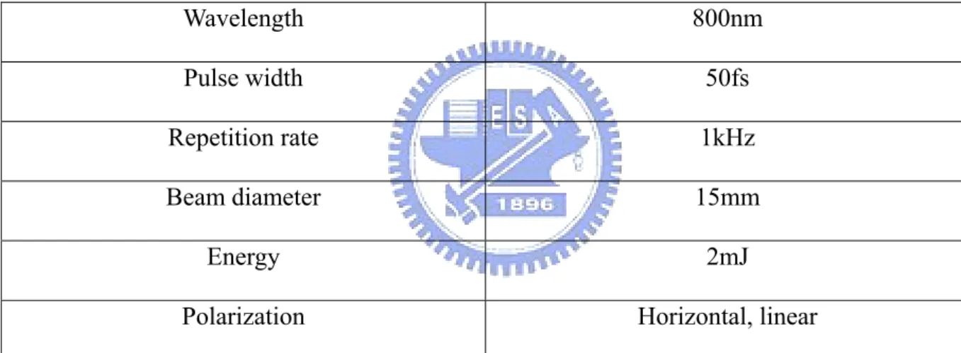
The pump laser for the amplification process in Spitfire is Q-switched Nd:YLF laser. This Nd:YLF laser delivers a high power output of 20W at 527 nm. The chirped-pulse amplification diagram is shown in Fig. 3-2. The Spitfire amplifies the seeding pulses by a million times from 6 nJ of energy per pulse to 2 mJ per pulse. The pulse repetition rate is 1kHz and the output power is 2W. The properties of the Ti:Sapphire regenerative amplifier is
shown in Table. 3-2.
Stretching
Amplification
Compression
Fig. 3-2. The chirped amplification process.
Wavelength 800nm
Pulse width 50fs
Repetition rate 1kHz
Beam diameter 15mm
Energy 2mJ
Polarization Horizontal, linear
3.2 The Terahertz Time-Domain Spectroscopy (THz-TDS)
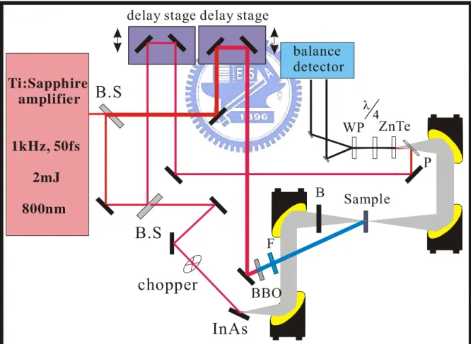
The optical layout of THz-TDS system is shown in Fig. 3-3 (schematic). An amplified Ti:sapphire laser source generating 50 fs, 800 nm, 2 mJ pulses at a repetition rate of 1 kHz is divided into pump and probe beams by a beam splitter. The first s-polarized 800 nm beam transmits a half-wave plate, turns to p-polarization, and then impinges on [100] p-type InAs surface in order to generate terahertz pulse predominantly by Photo-Dember effect. The second 800 nm beam is used to detect the electric field of the terahertz pulses using free-space electro-optic sampling in 2 mm-thick [110] ZnTe crystal. Any 800 nm beam reflects from the InAs surface is blocked by a black polyethylene sheet which has high transmissivity in the far-infrared. Gold-coated parabolic mirrors are used to collimate and focus the terahertz beam on the sample. The probe beam, which can be tuned the time delay by motor stage, is guided to the ZnTe crystal and the terahertz pulse collinearly impinged on ZnTe crystal. The transmitted laser pulse with polarization changed by electro-optical effect is separated into two beams with orthogonal polarizations by Wollaston beam splitter. These two beams are coupled to a balanced detector connecting to a lock-in amplifier. Signal from lock-in amplifier can be easily analyzed by a computer.
In order to reduce the water vapor absorption of THz signal, we cover the THz-TDS system with an acrylic box which is continuously infused with pure nitrogen. The humidity can be rapidly down to 5% in tens of minutes. Owing to the stable atmosphere and temperature, the THz system becomes more stable.
balance
detector
InAs
Sample
B.S
delay stage
chopper
ZnTe
4 λTi:Sapphire
amplifier
1kHz, 50fs
2mJ
800nm
P
WP
B
Fig. 3-3. The scheme of the terahertz pulse setup. BS: beam splitter; B: polyethylene visible
3.3 The Optical-Pump-Terahertz-Probe System (OPTP)
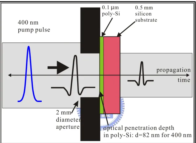
The extension of THz-TDS to OPTP is quite simple as shown in Fig. 3-4. Let laser beam pass through a beam splitter before the laser beam incident THz-TDS system, the reflected beam will incident into THz-TDS system and the transmitted beam is used as the optical pump beam. The optical pump beam induces the change in the sample and the resulting change in the terahertz transmission is measured. The optical pump beam is frequency doubled to 400 nm in a BBO crystal and used to excite the sample. Both the THz pump beam and the optical pump beam are passed through small pinhole at the center of two parabolic mirrors. Sample is fixed on the small pinhole and the incident angle of optical pump beam on the sample is . The spot size of the 400 nm pump beam is about 3 mm on the sample. The samples mount, as shown in Fig. 3-5, has a 2-mm-diameter aperture for uniform illumination of the sample with the pump beam and ensures good overlap between the pump beam and the THz probe beam.
o
5
The main advantage of OPTP is directly measure induced change in the far-infrared conductivity and refractive index in comparison to optical pump-probe method. Another advantage of OPTP is that it can measure the induced change of complex conductivity. Because the THz probe pulse is approximately 1 ps in duration, OPTP have lower sensitivity and the temporal resolution in comparison to optical pump-probe method.
There are two methods to acquire data in the OPTP experiment. The first method to observe dynamics is to set the time delay at a fixed value corresponding to the temporal position of the highest point of the main peak of the THz pulse. Then the dynamics are measured by scanning the optical pump delay line to map out the dynamics. This one-dimensional method measures the dynamics averaged over the frequency content of the THz pulse.
technique. We set the delay of the optical pump line at a fixed time delay, and then scan the THz waveform by THz-TDS. By measuring this waveform at different optical pump delay, it is possible to observe the evolution of the induced changes in the amplitude and phase of the THz electric field.
The transmission, T, of the amplitude of main peak of THz pulse was measured as the time delay between THz pulse and the 400 nm pump pulse. The differential transmission,
0 0 0 ) ( T T T T T = −
Δ where is the transmission of the amplitude of the main peak of the
THz pulse at negative time delays before the pump pulse has excited the sample.
0 T
balance
detector
InAs
F
Sample
B.S
B.S
delay stage delay stage
chopper
ZnTe
4 λTi:Sapphire
amplifier
1kHz, 50fs
2mJ
800nm
P
BBO
WP
B
Fig. 3-4. The scheme of the optical pump terahertz probe setup. B.S: beam splitter; B:
0.1 m
poly-Siµ 0.5 mmsilicon substrate
Fig. 3-5. The scheme of poly-Si and sample mount with 2mm-diameter aperture.
propagation
time
400 nm
pump pulse
2 mm
diameter
aperture
optical penetration depth
3.4 Calculated Method of Optical Constants for THz-TDS
We study the complex conductivity and optical constant from 0.4 to 2 THz by using THz-TDS system at certain optical pump time delay. The Drude model is used to fit the complex conductivity and optical constant.
We show the schematic sample in Fig.3-6, where E0(ω) is the incident electric field, )
(ω
ref
E is the transmitted electric field of the substrate, Efilm(ω) is the transmitted electric field of the film, d is the thickness of the film (the penetration of 82nm for crystalline silicon at 400nm). , and are the refractive indices. In our sample, =1, =3.41 is the refractive index of the silicon. The complex refractive index of the film is
1
n n2 n3 n1 n3
2
2 iκ
n + , where is the real refractive index and
2
n κ is the extinction coefficient. 2
)
(
0ω
E
)
(
ω
filmE
)
(ω
refE
)
(
0ω
E
d
n
1n
2n
3Fig. 3-6. The schematic sample between pump and unpump. n1, n2, n3 is the refractive indices.
E0(ω ) is the incident THz field. Eref(ω ) and Efilm(ω ) are the reference (without pump) and
) (ω
ref
E can be expressed as:
) ( ) exp( ) (ω 13 ω E0 ω c d i t Eref = . (1) Considering the multiple reflections in the film, the Efilm(ω) can be expressed as:
) ( ) 2 exp( 1 ) exp( ) ( 0 23 21 23 12 ω ω ω ω E c d n i r r c d in t t Efilm − = , (2)
where c is the speed of the light in vacuum, the and are the reflection and
transmission coefficient from i to j interface. We suppose that
ij
r tij
c d nω
<<1, because of our thin
film sample. We can simplify the equation (3) as:
] ) [( ) ( 1 ) ( ) ( 3 1 3 1 2 2 2 3 1 n n n n i n n n c d i E E ref film + + − − + + = ω κ ω ω . (3)
Equation (3) is expressed as exp( ) ) ( ) ( Δ − Α = i E E ref film ω ω
, where A and Δ are obtained from the
Fourier transformed reference and signal of THz pulse [32]. By using , the real and imaginary part of equation (4), (5) can be represented as:
2 2 2 " ' ε ( κ ) ε +i = n +i 3 1 3 1 3 1 ' (n n )Asin nn n n d c + Δ− + + = ω ε , (4) d c A n n ω ε" =( 1+ 3)(1− cosΔ) . (5)
Owing to the equation , the conductivity, real refractive index and the extinction coefficient can be deduced by:
2 2 2 " ' ε ( κ ) ε +i = n +i 2 1 2 " 2 ' ' 2 [ ] 2 1 ε + ε +ε = n , (6) 2 1 2 " 2 ' ' 2 [ ] 2 1 ε ε ε κ = − + + , (7)
)] ( [ " ' 0 + − ∞ =ωε ε ε ε σ i , (8)
where ε is the contribution of the bound electrons. The complex conductivity is deduced ∞
from Maxwell equation, assuming there exist a flowing current,Jr =σEv. The formula can be represented by: E i E i i E i J t D J H r r r r r r r ε ωε ωε σ ε ωε ε ωε 0 0 0 0 = ⎥ ⎦ ⎤ ⎢ ⎣ ⎡ + = + = ∂ ∂ + = × ∇ ∞ ∞ (9) 0 ωε σ ε ε i + = ∞
While the measured complex conductivity and complex refractivity index are obtained by multiple reflections, it is useful to use Drude model to describe transient conductivity.
3.5 Determination of Mobility and Conductivity from Drude Model
The Drude model, which was developed in the 1900s by Paul Drude [46], explains the transport properties of electrons in materials. It treats conduction electrons as free to move under the influence of an applied field. The Drude model can also predict conductivity as a response to time-dependent electric field with an angular frequency ω , the conductivity can be expressed as 0 0 2 0 1 ) ( ωτ τ ω ε ω σ i p − = . (10)
The plasma frequency is defined as =Ne m∗
p 0
2 ε
ω , where N is the carrier concentration, e
is the electronic charge, m* is the effective carrier mass and τ0 is the carrier scattering time. We can use complex conductivity by Drude model to fit the complex conductivity from multiple reflections. The two fitting parameters are plasma frequency, ωp, and carrier scattering time, τ =μm∗ e
0 , where μ is mobility. The fitting method is to find the least
mean square between σmultiple and σDrude in the frequency 0.4 – 2 THz, which can be represented as:
error
Drude multiple − =
∑
(σ σ )2 . (11)Chapter4 Properties and Preparation of Low Temperature Poly-Silicon
In the beginning of chapter 4, we introduce the properties of low temperature poly-silicon (LTPS). In section 4.2, our sample preparation, the recrystallization method of femtosecond-laser annealing (FLA) and laser annealing station are given in detail. In section 4.3, the characterizations of annealed sample are described.
4.1 Introduction of Low Temperature Poly-Silicon
Low temperature poly-silicon has attracted much attention resent year. With increasing the size of display and the pixel density of Thin Film Transistors – Liquid Crystal Display (TFT-LCD), the shorter charging time of pixel electrodes are needed. Therefore, higher mobility TFTs are required for pixel driver of TFT-LCD. However, due to the low mobility (0.5-1 cm2/Vs) of hydrogenated amorphous silicon (a-S:H), it is hard to achieve the requirement of TFTs. By introducing the poly-silicon film, the problem of low mobility for a-Si:H can be overcome. The poly-Si is the most promising material for possessing such high mobility TFTs for pixel drivers. Owing to the poly-Si, the peripheral driver circuits can be integrated on the same substrate. Fig. 4-1 shows the crystal structure and electrical characteristics performance comparison between different silicon structure thin films. In Fig. 4-1, we can clearly tell apart the difference between the amorphous silicon, poly-silicon, and single crystal silicon. The amorphous silicon is the non-crystalline form of silicon. Silicon atom has four atomic bonds which connected to four neighboring silicon atoms. This case also suitable for amorphous silicon, but amorphous silicon can not form a continuous crystalline lattice the same as the crystalline silicon. When the atom does not bond to four neighboring atoms, this atom has dangling bonds which are the defects in amorphous silicon. Owing to the dangling bonds in the continuous random network, these defects can be passivated by
introducing hydrogen into the silicon. It becomes hydrogenated amorphous silicon.
0.002~0.004
0.1
0.01
Lea kage Current
(p A / μm )
<0.1
1~4
2~5
Thres hold Vo ltage (V)500~600
30~300
0.5~1
M obility (cm2 / V-sec)Driver LSI
Driver Circuit
Pixel Sw itching
A pplication Crys tal StructureSing le crys tal Si
Poly-Si
amorpho us -Si
Grain Bo un dary
Fig. 4-1. The crystal structure and electrical characteristics performance comparison between
the silicon thin films.
Because of the low mobility of amorphous silicon, it is not suitable for the fast switch of TFTs. Fig. 4-1 shows the mobility relationship between the a-Si, poly-Si, and single crystal silicon. When there are many boundaries on the road, we can not drive fast. On the other hand, we can drive fast without any boundary. It is the same with the electron move in the three kinds of silicon. For a-Si, the electron need to pass through many boundaries on the road, the mobility is low. That is why the mobility of poly-Si is higher than the a-Si, and lower than the single crystal silicon. Although the mobility of single crystal silicon is higher than poly-Si, the conventional process temperature to manufacture the single crystal silicon film is over 1000 °C. Due to the melting point of the glass is about 500°C, we can not use the single crystal
silicon in TFT-LCD process. That is why we study poly-Si for TFTs.
In Fig. 4-1, we know the leakage current of three kinds of silicon. The single crystal silicon has lowest leakage current. Many group aim at studying the fabrication of high mobility, low leakage current and good uniformity for poly-Si. In order to reduce the flicker and cross-talk of TFT-LCD, poly-Si TFT with leakage current had been studied (below 1 pA/μm) [33].
Poly-Si
TFT-LCD
SOP
A-Si
TFT-LCD
Poly-Si
TFT-LCD
Gate Driver IC
Source Driver IC
Source PCB
Controller PCB
Control IC
Peripheral circuits
Source Driver IC
Fig. 4-2. Concepts of circuit integration. The comparison of a-Si TFT-LCD, poly-Si TFT-LCD
and poly-Si TFT-LCD system on panel. PCB means printed circuit board.
Because of the mobility of poly-Si is higher then a-Si, the higher extent of integration will be possible. It can make the integration of driver ICs onto the substrate possible due to high mobility. Then, the number of external connections and the size of substrate can be minimized. Fig. 4-2 shows the concept of circuit integration in TFT-LCDs. With decreasing the transistor of LCD by using poly-Si, the aperture ratio of poly-Si TFT-LCD and the screen
brightness can be increased significantly [34]. System on panel (SOP) technology, implementing memories, sensors, and controllers with driver circuits of displays on glass, will be realized in the future with poly-Si TFTs [35].
The conventional method to fabricate poly-Si is low pressure chemical vapor deposition (LPCVD) [36]. Because of the many disadvantages of LPCVD, such as high deposition temperature over 600°C and small grain size < 50nm, the solid phase crystallization (SPC) is used to increase the grain size in silicon. But SPC needs a long time annealing at high temperature over 600°C, it is also not suitable for glass substrate. Then, there is a liquid phase recrystallization method such as excimer laser annealing (ELA). ELA can achieve good quality poly-Si film [12-14]. This kind of laser-induced crystallization process can get good quality of poly-Si film.
4.2 Preparation of Poly-Silicon 4.2.1 Sample Preparation
The amorphous silicon samples were prepared by National Nano Device Laboratory (NDL). The amorphous silicon samples were fabricated by low pressure chemical vapor deposition (LPCVD). The scheme of LPCVD is shown in Fig. 4-3. The base of device is quartz tube in a spiral heater. This tube is evacuated to the pressure of 0.1 Pa and can be heated up to 1000°C. The chemical formula (1) of deposition is
SiH4 → Si + 2H2. (1)
The gas which is poured in tube consists of silane and the gas for dilution. The pressure in the tube is from 10 to 1000 Pa. Then, the amorphous silicon is deposited on the oxidized (500nm) silicon wafers at 550°C. The thickness of the amorphous silicon film is 100nm. The important factors that affect the thickness uniformity and the film content are positions of the substrates, temperature profile in the tube, reactor geometry, deposition time, working pressure and the content of the poured gas.
4.2.2 Femtoseoncd Laser Annealing (FLA)
We use near-infrared femtosecond laser to anneal the a-Si:H. The intense femtosecond laser pulses lead to efficient nonlinear photon absoption in irradiated materials, enabling a melting of amorphous silicon films. On excitation with a femtosecond pulses, a semiconductor undergoes several stages of relaxation before returning to equilibrium. The energy is transferred first to the electrons and then to the lattice.
Mechanisms of femtosecond laser-induced ablation on crystalline silicon are investigated by time-resolved pump-and-probe microscopy in normal imaging and shadowgraph arrangements. The imaging with the time-delayed frequency-doubled probe beam had a temporal resolution of 100 fs. The high electron temperatures and dense solid-state plasma formation suggest a non-equilibrium phase transition process. Thermionic emission and photoemission of electrons can initiate air plasma in the proximity of the surface. Time-resolved shadowgraphs of the shock wave propagation show that the ultrafast initial plasma becomes visible at around 10 ps and is followed by a slower ‘‘thermal’’ contribution in the time scale of 30 ns. The instantaneous energy released upon initiation of explosion is estimated to be 10%–17% of the absorbed laser energy depending on the incident laser energy. [38].
Femtosecond laser annealing (FLA) assisted by a scanning of laser beam efficiently crystallizes amorphous silicon films with large average grains of 800nm, using a total laser energy as low as ~ 0.9J/cm2 [39]. Up to now, a clear distinction of the transition between the ultrafast liquid phase and the electron-hole plasma state is hard. However, it is undoubted that the classical thermal model of crystallization mediated cannot explain the subpicosecond rapid phase transition satisfactorily.
4.2.3 The Laser Annealing Station
The scheme of the laser annealing apparatus is shown in Fig. 4-4. A femtosecond laser beam of 50 fs pulse duration and 800 nm of central wavelength are guided into the chamber. Then, this beam is focused on the sample in the chamber by a convex lens with length of 10 cm. The focus area on the sample is in the strip spot (105μm × 2850μm).
Silane-based a-Si films (100nm) are deposited on the oxidized (500nm) silicon wafers by LPCVD. The samples are placed on flat-top building in the vacuum chamber. The working temperature of the flat-top building is warmed up to 395°C. In our annealing experiment, the overlapping of the laser beam is fixed at 95% (i.e. 5.25 mm/s, or equivalently 20 laser shots per unit area) [39].
1
kHz Reg. Amp
(800nm, 50fs)
Beam expander
M
M
M
M
M
M
M
M:IR dielectric mirror
control stage
Transition stage
Vaccum chamber
4.3 Characterization of Annealing Samples
In our experiment, we prepare two samples with the same annealing conditions in addition to the annealed power. Due to the different annealed power, the different grain size of poly-Si can be prepared. The scanning electron microscope (SEM) pictures of the annealing areas with obvious grain boundary, which delineate the defect in the silicon film, obtained by using secco etching. The average grain size of poly-Si (sample A) in Fig. 4-5(a) is about 500 nm with annealed fluence 40±0.5 mJ/cm2. The average grain size of poly-Si (sample B) in Fig. 4-5(b) is about 50 nm with annealed fluence 35±0.5 mJ/cm2.
( )
a
( )
b
Fig. 4-5. SEM images of FLA poly-silicon samples after Secco etching for scanned FLA (a)