536 IEEE TRANSACTIONS ON CIRCUITS AND SYSTEMS FOR VIDEO TECHNOLOGY, VOL. 11, NO. 4, APRIL 2001
An Efficient Architecture for Two-Dimensional
Discrete Wavelet Transform
Po-Cheng Wu and Liang-Gee Chen, Fellow, IEEE
Abstract—This paper proposes an efficient architecture for
the two-dimensional discrete wavelet transform (2-D DWT). The proposed architecture includes a transform module, a RAM module, and a multiplexer. In the transform module, we employ the polyphase decomposition technique and the coefficient folding technique to the decimation filters of stages 1 and 2, respectively. In comparison with other 2-D DWT architectures, the advantages of the proposed architecture are 100% hardware utilization, fast computing time (0.5–0.67 times of the parallel filters’), regular data flow, and low control complexity, making this architecture suitable for next generation image compression systems, e.g., JPEG-2000.
Index Terms—Decimation filters, discrete wavelet transform,
image compression, JPEG-2000, multirate digital signal pro-cessing.
I. INTRODUCTION
W
ITH the rapid progress of VLSI design technologies, many processors based on audio and image signal pro-cessing have been developed recently. The two-dimensional dis-crete wavelet transform (2-D DWT) plays a major role in the JPEG-2000 image compression standard [1]. Presently, research on the DWT is attracting a great deal of attention [2]–[6]. In addition to audio and image compression [7]–[10], the DWT has important applications in many areas, such as computer graphics, numerical analysis, radar target distinguishing and so forth. The architecture of the 2-D DWT is mainly composed of the multirate filters. Because extensive computation is in-volved in the practical applications, e.g., digital cameras, high-efficiency and low-cost hardware is indispensable.At present, many VLSI architectures for the 2-D DWT have been proposed to meet the requirements of real-time processing. However, because the filtering operations are required in both the horizontal and vertical directions, designing a highly effi-cient architecture at a low cost is difficult. Lewis and Knowles [11] used the four-tap Daubechies filter to design a 2-D DWT ar-chitecture. Parhi and Nishitani [12] proposed two architectures that combine the word-parallel and digital-serial methodologies. Chakrabarti and Vishwanath [13] presented the nonseparable ar-chitecture and the SIMD array arar-chitecture. Vishwanath et al. [14] employed two systolic array filters and two parallel filters to implement the 2-D DWT. The modified version uses four
par-Manuscript received June 3, 1999; revised August 11, 2000. This paper was recommended by Associate Editor J.-N. Hwang.
P.-C. Wu is with the Information Technology Division, Institute for Informa-tion Industry, Taipei, Taiwan, R.O.C. (e-mail: pcwu@netrd.iii.org.tw).
L.-G. Chen is with the Department of Electrical Engineering, National Taiwan University, Taipei, Taiwan, R.O.C. (e-mail: lgchen@cc.ee.ntu.edu.tw).
Publisher Item Identifier S 1051-8215(01)03013-0.
allel filters as reported in [15] and [16]. Chuang and Chen [17] proposed a parallel pipelined VLSI array architecture for the 2-D DWT. Chen and Bayoumi [18] presented a scalable systolic array architecture. Other 2-D DWT architectures have been re-ported in [19]–[23].
Among the various architectures, the best-known design for the 2-D DWT is the parallel filter architecture [15], [16]. The design of the parallel filter architecture is based on the modified recursive pyramid algorithm (MRPA) [13], which intersperses the computation of the second and following levels among the computation of the first level. The MRPA is feasible for the 1-D DWT architecture, but is not suitable for the 2-D DWT, because the hardware utilization is inefficient and a complicated control circuit results from the interleaving data flow. Therefore, in this paper, we propose a new VLSI architecture for the separable 2-D DWT. The advantages of the proposed architecture are the 100% hardware utilization, fast computing time, regular data flow, and low control complexity. Additionally, because of the regular structure, the proposed architecture can easily be scaled with the filter length and the 2-D DWT level.
This paper is organized as follows. Section II introduces the 2-D DWT algorithm. Section III discusses the previous design techniques. In Section IV, an efficient architecture for the 2-D DWT is proposed. Section V compares the performance of var-ious 2-D DWT architectures. Finally, we state our conclusions in Section VI.
II. 2-D DWT ALGORITHM
The proposed architecture deals with the separable 2-D DWT, whose mathematical formulas are defined as follows:
(1)
(2)
(3)
(4)
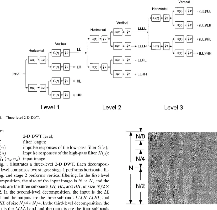
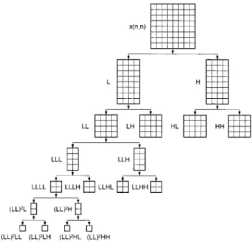
Fig. 1. Three-level 2-D DWT.
where
2-D DWT level; filter length;
impulse responses of the low-pass filter ; impulse responses of the high-pass filter ; input image.
Fig. 1 illustrates a three-level 2-D DWT. Each decomposi-tion level comprises two stages: stage 1 performs horizontal fil-tering, and stage 2 performs vertical filtering. In the first-level decomposition, the size of the input image is , and the outputs are the three subbands LH, HL, and HH, of size
. In the second-level decomposition, the input is the LL band and the outputs are the three subbands LLLH, LLHL, and
LLHH, of size . In the third-level decomposition, the input is the LLLL band and the outputs are the four subbands
LL LL LL LH LL HL, and LL HH, of size
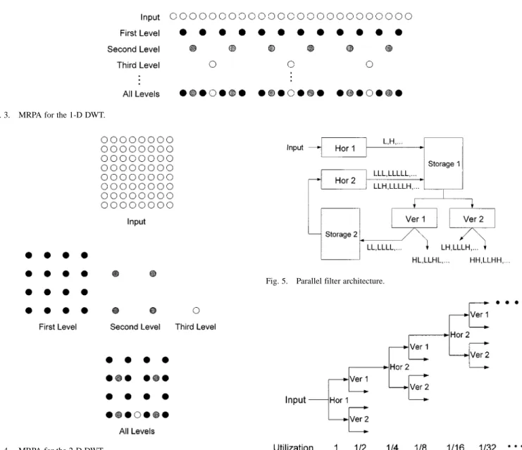
. The multi-level 2-D DWT can be extended in an analo-gous manner. Fig. 2 shows the result of the “Lena” image after a three-level 2-D DWT.
III. PREVIOUSTECHNIQUES
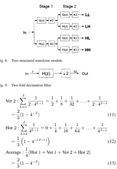
At present, the best-known architecture for the 2-D DWT is the parallel filter architecture [15], [16]. The design of the par-allel filter architecture is based on the MRPA [13]. The MRPA is initially proposed for the 1-D DWT architectures. As illustrated in Fig. 3, the MRPA intersperses the computation of the second and following levels among the computation of the first level. Because of the decimation operation, the quantity of processing data in each level is half of that in the previous level. The total quantity of processing data can be counted as follows:
(5)
Fig. 2. Result of the “Lena” image after a three-level 2-D DWT.
where
1-D DWT level;
quantity of processing data in the first level; that of the second level;
.. .
that of the th level.
Hence, if the 1-D DWT level is large enough, (5) will become (6) Because the quantity of processing data in the second and fol-lowing levels (i.e., ) is the same as that in the first level (i.e., ), the computing time of the first level can be filled as shown in Fig. 3. The hardware utilization is efficient. Hence, the MRPA is feasible for the 1-D DWT architectures.
However, as illustrated in Fig. 4, we find that the MRPA is not suitable for the 2-D DWT architectures. Since the quantity of processing data in each level is a quarter of that in the previous
538 IEEE TRANSACTIONS ON CIRCUITS AND SYSTEMS FOR VIDEO TECHNOLOGY, VOL. 11, NO. 4, APRIL 2001
Fig. 3. MRPA for the 1-D DWT.
Fig. 4. MRPA for the 2-D DWT.
level, the total quantity of processing data is counted as follows:
(7) where
2-D DWT level;
quantity of processing data in the first level; that of the second level;
.. .
that of the th level.
If the 2-D DWT level is large enough, (7) will become (8) Because the quantity of processing data in the second and fol-lowing levels (i.e., ) is only one third of that in the first level (i.e., ), the computing time of the first level cannot be
Fig. 5. Parallel filter architecture.
Fig. 6. Job allocation of the parallel filter architecture.
filled, as shown in Fig. 4. Hence, the hardware utilization is efficient, and a complicated control circuit results from the in-terleaving data flow.
Fig. 5 illustrates the parallel filter architecture, which is com-posed of four filters (Hor 1, Hor 2, Ver 1, and Ver 2) and two transpose memories (Storage 1 and Storage 2) for row–column transposition. Hor 1 performs the horizontal filtering of the first level. Hor 2 performs the horizontal filtering of the second and following levels. Ver 1 and Ver 2 perform the vertical filtering of all levels.
Fig. 6 shows the job allocation of the parallel filter architec-ture. According to Fig. 6, we can compute the individual and average hardware utilization of these four filters for different 2-D DWT levels as follows:
Hor (9)
Ver
TABLE I
HARDWAREUTILIZATION OF THEPARALLELFILTERARCHITECTURE FORDIFFERENT2-D DWT LEVELS
Fig. 7. Proposed 2-D DWT architecture.
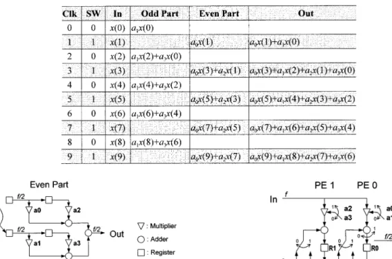
Fig. 8. Tree-structured transform module.
Fig. 9. Two-fold decimation filter.
Ver
(11) Hor
(12)
Average Hor Ver Ver Hor
(13) where is the 2-D DWT level.
Table I lists the hardware utilization of the parallel filter ar-chitecture for different 2-D DWT levels. In one-level 2-D DWT, the hardware utilization of the parallel filter architecture is only 50%. As the 2-D DWT level increases, the utilization converges to 66.67%. Because of inefficient hardware utilization, the par-allel filter architecture requires a longer computing time, the
main problem of the parallel filter architecture as well as the present 2-D DWT architecture design.
IV. PROPOSED2-D DWT ARCHITECTURE
The block diagram of the proposed 2-D DWT architecture is shown in Fig. 7, which includes a transform module, a RAM module, and a multiplexer. The size of the RAM module is . The decomposition scheme is level by level and described as follows. In the first-level decomposition, the multiplexer selects data from the input image. The transform module decomposes the input image to the four subbands LL,
LH, HL, and HH, and saves the LL band to the RAM module.
After finishing the first-level decomposition, the multiplexer selects data from the RAM module. The LL band is then sent into the transform module to perform the second-level decomposition. The transform module decomposes the LL band to the four subbands LLLL, LLLH, LLHL, and LLHH, and saves the LLLL band to the RAM module. After finishing the second-level decomposition, the multiplexer selects data from the RAM module. The LLLL band is then sent into the transform module to perform the third-level decomposition. The transform module decomposes the LLLL band to the four
subbands LL LL LL LH LL HL, and LL HH, and
saves the LL LL band to the RAM module. This procedure repeats until the desired level (i.e., the last level) is finished.
The advantage of such a scheme is that the data flow is very regular. We can concentrate our effort to efficiently design the transform module. As shown in Fig. 8, the transform module is tree-structured and comprises two stages. Stage 1 performs horizontal filtering, and stage 2 performs vertical filtering. To design the transform module efficiently, we assume “ ” to be the area cost and “ ” to be the time cost required in stage 1. According to the original design as shown in Fig. 8, the number of filters required in stage 2 is double that of stage 1. That is, is the area cost required in stage 2. On the other hand, because of the decimation operation in stage 1, the quantity of data for filtering in each filter of stage 2 is half that of stage 1. Hence, the computing time required in stage 2 is half of , i.e., . Since stage 2 is cascaded after stage 1, stage 2 can not work until stage 1 finishes its job. Therefore, we find that there will
be hardware idle in stage 2. In other words,
the hardware utilization in the original design is inefficient. In order to solve this problem, we consider a single decima-tion filter as shown in Fig. 9. The frequency labels “ ” and
540 IEEE TRANSACTIONS ON CIRCUITS AND SYSTEMS FOR VIDEO TECHNOLOGY, VOL. 11, NO. 4, APRIL 2001
TABLE II
DATAFLOW OF THEDECIMATIONFILTEREMPLOYING THEPOLYPHASEDECOMPOSITIONTECHNIQUE. (SW : DIRECTIONS OF THESWITCH)
Fig. 10. Decimation filter employing the polyphase decomposition technique.
“ ” imply that the output frequency is half the input fre-quency. The decimation filter can be implemented directly by a filter followed by a two-folded decimator. However, the deci-mator discards one sample out of every two samples at the filter output, causing poor hardware utilization. Hence, we employ two different design techniques to enhance its performance. The first technique is the polyphase decomposition technique as il-lustrated in Fig. 10, which decomposes the filter coefficients into even-ordered and odd-ordered parts. In the even clock cy-cles, the input data are fed to the odd part and multiplied with the odd-ordered coefficients. In the odd clock cycles, the input data are fed to the even part and multiplied with the even-ordered coefficients. The output data are the sum of the odd and even parts. The internal clock rate is half the input clock rate after employing the polyphase decomposition technique. Therefore, we can double the input clock rate to increase the throughput. When the quantity of processing data is the same, the computing time will be reduced to half. Thus, this technique can reduce the time cost to a half. We use the symbol “ ” to represent the polyphase decomposition technique. Table II shows the data flow of the decimation filter employing the polyphase decom-position technique.
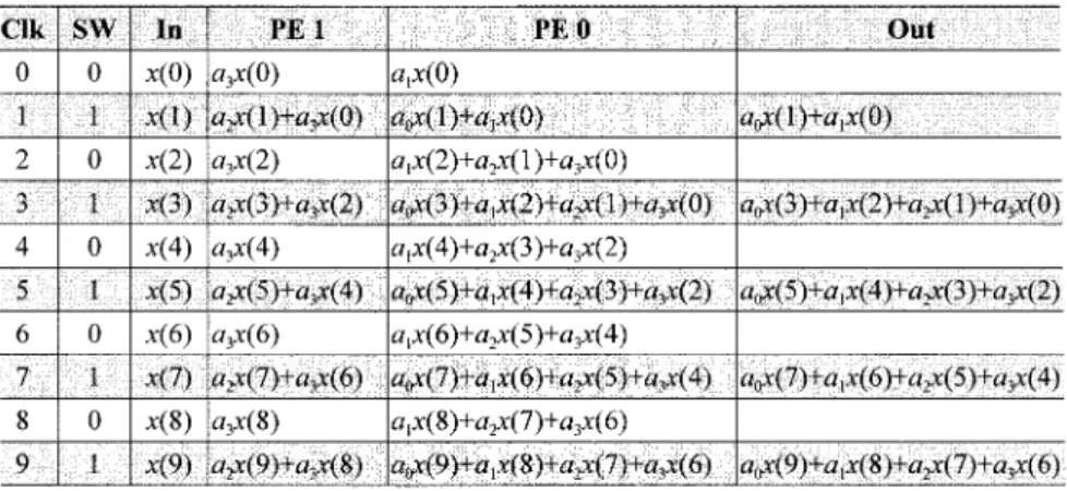
The second technique is the coefficient folding technique. As illustrated in Fig. 11, every two coefficients share one set of a multiplier, adder, and register. The switches control the data path. The operation of Fig. 11 is described as follows. Viewing the PE0 first, in clock-cycle 0, the input data is multiplied with the coefficient and added with the con-tent of R1 (initially zero). The result is then stored to R0. In clock-cycle 1, the input data is multiplied with the coefficient and added with the content of R0, i.e., .
Fig. 11. The decimation filter employing the coefficient folding technique.
The result is then output. In clock-cycle 2,
the input data is multiplied with the coefficient and
added with the content of R1, i.e., . The result
is then stored to R0. In clock-cycle 3, the input data is multiplied with the coefficient and
added with the content of R0, i.e., .
The result is then output. The
following clock cycles are arranged in an analogous manner. The operation of the PE1 is similar to the PE0. Because every two coefficients share one set of a multiplier, adder, and register, this technique can approximately reduce the area cost to a half. We use the symbol “ ” to represent the coefficient folding technique. Table III shows the data flow of the decimation filter employing the coefficient folding technique.
Now, we employ these two design techniques to the decima-tion filters of stages 1 and 2, respectively. Hence, four different design methods are derived for the transform module. The de-sign strategy (including the original dede-sign) is listed in Table IV. From Table IV, we find that if we employ the polyphase decom-position technique to stage 1 and the coefficient folding tech-nique to stage 2, the area and time cost will both be the same and in stages 1 and 2. Thus, the total area cost is and the total time cost is . The AT product is reduced from to , and no hardware is idle in stage 2. Therefore, the perfor-mance of the new design method is three times more efficient than the original design. In contrast, the other design methods, as listed in Table IV, cause the hardware to be idle in stage 2. Hence, they are not efficient design schemes.
In stage 2 of the transform module, because the image data are fed by a raster-scan mode, each coefficient requires a line delay to store the row data for vertical filtering. Therefore, the regis-ters in Fig. 11 need to be replaced with the line delays for
ver-TABLE III
DATAFLOW OF THEDECIMATIONFILTEREMPLOYING THECOEFFICIENTFOLDINGTECHNIQUE. (SW : DIRECTIONS OF THESWITCHES)
TABLE IV
DESIGNSTRATEGY OF THETRANSFORMMODULE. (T=2: POLYPHASEDECOMPOSITIONTECHNIQUE;A=2: COEFFICIENTFOLDINGTECHNIQUE)
TABLE V
DATAFLOW OF THEMODIFIEDDECIMATIONFILTEREMPLOYING THECOEFFICIENTFOLDINGTECHNIQUE FORVERTICALFILTERING. (SW : DIRECTIONS OF THESWITCHES;N: LENGTH OF THEROW;x (n): nTHROWDATA)
Fig. 12. The modified decimation filter employing the coefficient folding technique for vertical filtering.
tical filtering. Fig. 12 shows the modified result. The data flow is shown in Table V where represents the th row data.
Every two input rows generate one output row. Fig. 13 shows the structure of the line delay, which is composed of select
sig-nals, , and storage
blocks of size .
The size of the line delay in the different decomposition levels is described below.
In the first-level decomposition, the select signal is en-abled, and the others are disabled. The size of the line delay is the sum of all storage blocks as follows:
542 IEEE TRANSACTIONS ON CIRCUITS AND SYSTEMS FOR VIDEO TECHNOLOGY, VOL. 11, NO. 4, APRIL 2001
(a)
(b)
Fig. 13. (a) Line delay with select signals to change its size to
N=2; N=4; N=8; . . . ; N=2 in the different decomposition levels. (b) The 1 to 2 demultiplexer used in the line delay.
Fig. 14. Transform module employing the polyphase decomposition technique to stage 1 and the coefficient folding technique to stage 2.
Fig. 15. Three-level 2-D DWT in the proposed architecture. The decomposition begins with an 8 2 8 block in the first level, and ends with four1 2 1 pixels in the third level.
Thus, it can store the row data output from the decimation filter of stage 1. In the second-level decomposition, the select signal is enabled, and the others are disabled. The size of the line delay is the sum of the previous storage blocks as follows: (15) In the following decomposition levels, the select signals change the size of the line delay to in the third level, in the
fourth level in the th level, in the
th level.
Assume that the low-pass filter has four taps: ,
and , and the high-pass filter has four taps: ,
and . Fig. 14 illustrates the transform module employing both the polyphase decomposition and the coefficient folding techniques. The frequency labels “ ,” “ ,” and “ ” imply that the output frequency is a quarter of the input frequency. In stage 1, because we use the FIR direct-form to implement the polyphase decomposition technique, the low- and high-pass decimation filters can share the same registers. Here, we have assumed that the filters in stages 1 and 2 have the same length, but in practice, this condition is not necessary for the correct operation. In addition, because we employ the polyphase decomposition technique in the decimation filters of stage 1, the internal clock rate of the transform module is half the input clock rate. Fig. 15 illustrates the three-level 2-D DWT in the proposed architecture. The decomposition begins with an block in the first level, and ends with four pixels in the third level. Table VI shows the data flow according to the ports of the transform module. The clock cycles 0–63 perform the first-level decomposition, the clock cycles 64–79 perform the second-level decomposition, and the clock cycles 80–83 perform the third-level decomposition. Because of the regular structure, the proposed architecture can be easily scaled with the filter length and the 2-D DWT level.
TABLE VI DATAFLOW OFFIG.15
V. PERFORMANCECOMPARISONS
The typical 2-D DWT architectures include the parallel filter architecture [16], direct architecture [14], nonseparable archi-tecture [13], SIMD archiarchi-tecture [13], and systolic-parallel ar-chitecture [14]. In Table VII, we compare the performance of our architecture and these 2-D DWT architectures in terms of the number of multipliers, the number of adders, storage size, computing time, control complexity, and hardware utilization. The computing time has been normalized to the same internal
clock rate. The parameter is the filter length, is the image size, and is the 2-D DWT level. The computing time of our architecture is derived as follows:
544 IEEE TRANSACTIONS ON CIRCUITS AND SYSTEMS FOR VIDEO TECHNOLOGY, VOL. 11, NO. 4, APRIL 2001
TABLE VII
PERFORMANCECOMPARISONS OFVARIOUS2-D DWT ARCHITECTURES. (K: FILTERLENGTH;N : IMAGESIZE;ANDJ: 2-D DWT LEVEL)
Fig. 16. Computing time of the proposed architecture and the parallel filter architecture for different 2-D DWT levels.
where the factor is because the internal clock rate of our ar-chitecture is half the input clock rate. Therefore, if our architec-ture and other architecarchitec-tures have the same internal clock rate, the throughput of our architecture is twice that of other archi-tectures. To do this, doubling the input clock rate for the pixel input can be used. The outcome of the comparisons shows that our design outperforms other architectures, especially in com-puting time, control complexity, and hardware utilization.
We also compare the computing time and the hardware uti-lization between our architecture and the parallel filter archi-tecture [16] for different 2-D DWT levels. The design of the parallel filter architecture is based on the MRPA, which in-tersperses the computation of the second and following levels among the computation of the first level. Fig. 16 plots the com-puting time for different 2-D DWT levels, showing that in one-level 2-D DWT , the computing time of our
architec-ture is clock cycles. As the 2-D
DWT level increases , the computing time converges
to clock cycles. In contrast, the
parallel filter architecture always requires the computing time of clock cycles. On the other hand, as shown in Table I, the hardware utilization of the parallel filter architecture is only
50% in one-level 2-D DWT . As the 2-D DWT level
increases , the utilization converges to 66.67%. How-ever, our architecture can consistently maintain 100% hardware utilization.
Concerning the storage size, the proposed architecture re-quires a RAM module of size to save the intermediate data. However, because the proposed architecture is mainly ap-plied in the image compression systems, it can use the memory
already existing in the systems to save the intermediate data. Hence, in this condition, the proposed architecture will not re-quire the RAM module. The remain storage size is , where is the line delays required in stage 2 for vertical fil-tering, and is the registers required in stage 1 for horizontal filtering.
VI. CONCLUSION
In recent years, many 2-D DWT architectures have been pro-posed to meet the requirements of real time processing. How-ever, the hardware utilization of these architectures needs to be further improved. Therefore, in this paper, we have proposed an efficient architecture for the 2-D DWT. The proposed ar-chitecture has been correctly verified by the Verilog Hardware Description Language (Verilog HDL). The advantages of the proposed architecture are the 100% hardware utilization, fast computing time, regular data flow, and low control complexity, making this design suitable for next generation image compres-sion systems, e.g., JPEG-2000.
REFERENCES
[1] Coding of Still Pictures: JPEG 2000 Part I Final Committee Draft
Ver-sion 1.0, ISO/IEC JTC 1/SC 29/WG 1 (ITU-T SG8), Mar. 2000.
[2] S. G. Mallat, “A theory for multiresolution signal decomposition: The wavelet representation,” IEEE Trans. Pattern Anal. Machine Intell., vol. 11, pp. 674–693, July 1989.
[3] , “Multifrequency channel decompositions of image and wavelet models,” IEEE Trans. Acoust., Speech, Signal Processing, vol. 37, pp. 2091–2110, Dec. 1989.
[4] P. P. Vaidyanathan, Multirate Systems and Filter Banks. Englewood Cliffs, NJ: Prentice-Hall, 1993.
[5] M. Vetterli and J. Kovacevic, Wavelets and Subband Coding. Englewood-Cliffs, NJ: Prentice Hall, 1995.
[6] G. Strang and T. Q. Nquyen, Wavelets and Filter Banks. Cambridge, MA: Wellesley-Cambridge Press, 1996.
[7] E. B. Richardson and N. S. Jayant, “Subband coding with adaptive pre-diction for 56 kbits/s audio,” IEEE Trans. Acoust., Speech, Signal
Pro-cessing, vol. ASSP-34, pp. 691–696, Aug. 1986.
[8] J. W. Woods and S. D. O’Neil, “Subband coding of images,” IEEE Trans.
Acoust., Speech, Signal Processing, vol. ASSP-34, pp. 1278–1288, Oct.
1986.
[9] J. Shapiro, “Embedded image coding using zerotrees of wavelet coef-ficients,” IEEE Trans. Signal Processing, vol. 41, pp. 3445–3462, Dec. 1993.
[10] A. Said and W. A. Pearlman, “A new fast and efficient image codec based on set partitioning in hierarchical trees,” IEEE Trans. Circuits
Syst. Video Technol., vol. 6, pp. 243–250, June 1996.
[11] A. S. Lewis and G. Knowles, “VLSI architecture for 2-D Daubechics wavelet transform without multipliers,” Electron. Lett., vol. 27, pp. 171–173, Jan. 1991.
[12] K. K. Parhi and T. Nishitani, “VLSI architectures for discrete wavelet transforms,” IEEE Trans. VLSI Syst., vol. 1, pp. 191–202, June 1993.
[13] C. Chakrabarti and M. Vishwanath, “Efficient realization of the discrete and continuous wavelet transforms: From single chip implementations to mappings on SIMD array computers,” IEEE Trans. Signal Processing, vol. 43, pp. 759–771, Mar. 1995.
[14] M. Vishwanath, R. M. Owens, and M. J. Irwin, “VLSI architectures for the discrete wavelet transform,” IEEE Trans. Circuits Syst. II, vol. 42, pp. 305–316, May 1995.
[15] C. Chakrabarti and C. Mumford, “Efficient realizations of analysis and synthesis filters based on the 2-D discrete wavelet transform,” in Proc.
IEEE ICASSP, May 1996, pp. 3256–3259.
[16] C. Chakrabarti and M. Vishwanath, “Architectures for wavelet trans-forms: A survey,” J. VLSI Signal Processing, vol. 14, pp. 171–192, 1996. [17] H. Y. H. Chuang and L. Chen, “VLSI architecture for fast 2-D discrete orthonormal wavelet transform,” J. VLSI Signal Processing, vol. 10, pp. 225–236, 1995.
[18] J. Chen and M. A. Bayoumi, “A scalable systolic array architecture for 2-D discrete wavelet transforms,” in Proc. IEEE VLSI Signal Processing
Workshop, 1995, pp. 303–312.
[19] R. Rumian, “An architecture for real-time wavelet image decomposi-tion,” Proc. IEEE Int. Symp. Circuits and Systems, pp. 73–76, May 1994. [20] T. C. Denk and K. K. Parhi, “Calculation of minimum number of regis-ters in 2-D discrete wavelet transforms using lapped block processing,”
Proc. IEEE Int. Symp. Circuits and Systems, pp. 77–81, May 1994.
[21] J. Bae and V. K. Prasanna, “Synthesis of VLSI architecture for two di-mensional discrete wavelet transforms,” in Proc. IEEE Int. Conf.
Appli-cation Specific Array Processors, July 1995, pp. 174–181.
[22] J. C. Limqueco and M. A. Bayoumi, “A VLSI architecture for separable 2-D discrete wavelet transforms,” J. VLSI Signal Processing, vol. 18, pp. 125–140, 1998.
[23] G. Lafruit, F. Catthoor, J. P. H. Cornelis, and H. J. D. Man, “An efficient VLSI architecture for 2-D wavelet image coding with novel image scan,”
IEEE Trans. VLSI Syst., vol. 7, pp. 56–68, Jan. 1999.
Po-Cheng Wu received the B.S. degree in computer
science and information engineering from National Chiao Tung University, Hsinchu, Taiwan, in 1991, and the M.S. and Ph.D. degrees in electrical engi-neering from National Taiwan University, Taipei, Taiwan, in 1994 and 1999, respectively.
He is currently a Senior Engineer at the Institute for Information Industry, Taipei, Taiwan. His major research interests include DSP architecture design, video coding, and multimedia networking.
Dr. Wu received Acer’s Long-Term Paper Award and Xerox’s Academic Paper Award, both in 1994. In 1999, he received the Best Paper Award of the IEEE Workshop on Consumer Electronics.
Liang-Gee Chen (S’84–M’86–SM’94–F’00) received the B.S., M.S., and Ph.D. degrees in electrical engineering from National Cheng Kung University, Tainan, Taiwan, in 1979, 1981, and 1986, respectively.
He was an Associate Professor during 1986–1988 in the Department of Electrical Engineering, National Cheng Kung University. In 1988, he joined the De-partment of Electrical Engineering, National Taiwan University. During 1993–1994 he was a Visiting Con-sultant at the DSP Research Department, AT&T Bell Labs, Murray Hill, NJ. In 1997, he was a Visiting Scholar of the Department of Electrical Engineering, University of Washington at Seattle. Currently, he is a Professor at National Taiwan University. His current research interests are DSP architecture design, video processor design, and video-coding systems.
Dr. Chen was the General Chairman of the 7th VLSI Design/CAD Sympo-sium and is currently the General Chairman of the 1999 IEEE Workshop on Signal Processing Systems: Design and Implementation. He has served as As-sociate Editor of IEEE TRANSACTIONS ONCIRCUITS ANDSYSTEMS FORVIDEO TECHNOLOGYsince June 1996, and Associate Editor of IEEE TRANSACTIONS ONVERYLARGESCALEINTEGRATIONSYSTEMSsince January 1999. He was the Associate Editor of the Journal of Circuits, Systems, and Signal Processing since 1999, and previously served as the Guest Editor of the Journal of Signal
Processing Systems. He received the Best Paper Award from the R.O.C.
Com-puter Society in 1990 and 1994, the Long-Term (Acer) Paper Award annually from 1991 to 1999, the Best Paper Award of the Asia-Pacific Conference on Cir-cuits and Systems in the VLSI Design track in 1992, the Annual Paper Award of Chinese Engineer Society in 1993, and in 1996, the Outstanding Research Award from NSC and the Dragon Excellence Award for Acer. He is a member of Phi Tan Phi.