國 立 交 通 大 學
電子工程學系 電子研究所
博 士 論 文
新穎低溫複晶矽薄膜電晶體與前瞻非揮發性
記憶體元件之製作與特性研究
Fabrication and Characterization of Novel
Low Temperature Polycrystalline Silicon Thin-Film
Transistors and Advanced Nonvolatile Memory
研 究 生 :涂 峻 豪
指導教授 :張 俊 彥 院 士
張 鼎 張 博 士
新穎低溫複晶矽薄膜電晶體與前瞻
非揮發性記憶體元件之製作與特性研究
Fabrication and Characterization of Novel
Low Temperature Polycrystalline Silicon Thin-Film
Transistors and Advanced Nonvolatile Memory
研 究 生 :涂 峻 豪
Student: Chun-Hao Tu
指導教授 :張 俊 彥 院 士
Advisor: Dr. Chun-Yen Chang
張 鼎 張 博 士 Dr. Ting-Chang Chang
國 立 交 通 大 學
電子工程學系 電子研究所
博 士 論 文
A Dissertation
Submitted to Department of Electronics Engineering and
Institute of Electronics
College of Electrical Engineering and Computer Engineering
National Chiao Tung University
In Partial Fulfillment of the Requirements
For the Degree of
Doctor of Philosophy
in
Electronics Engineering
March 2007
Hsinchu, Taiwan, Republic of China
中華民國九十六年三月
新穎低溫複晶矽薄膜電晶體與前瞻非揮發性
記憶體元件之製作與特性研究
研究生: 涂峻豪
指導教授: 張俊彥 院士
張鼎張 博士
國立交通大學
電子工程學系 電子研究所博士班
中文摘要 中文摘要中文摘要 中文摘要 本論文首先提出以鈍化方式來提昇低溫複晶矽薄膜電晶體(Poly-Si TFTs)的特 性以及元件的可靠度。本論文提出在非晶矽薄膜沈積後,以氟(F)離子佈植的方 式,先預先植入非晶矽薄膜中,其佈植劑量為 5×1013 cm-2。經過傳統的固態結晶 技術(SPC)之後,再進行後續的元件製作。我們發現經過氟離子佈植過後的複 晶矽薄膜電晶體其元件特性相較於傳統的固態結晶的薄膜電晶體,有比較低的起 始電壓(VTH),較低的次臨界導通特性(S.S),以及較高的載子移動率(µFE)。此乃由 於氟離子佈植會降低複晶矽薄膜中本身的缺陷(trap),包括淺能階(tail state)以及 深能階(deep state)的缺陷,進而提昇元件的特性。相較於傳統的氟離子佈植的鈍 化方法,在做熱結晶前並沒有額外的氧化層沈積。經過固態熱結晶後,薄膜中的 氟離子會聚積到複晶矽的表面,以及複晶矽與緩衝氧化層(buffer oxide)的介面, 此乃氟離子會受熱而往氧化層聚積。複晶矽表面的原生氧化層(native oxide)同時 也具有使氟離子聚積的驅動力。這不但可以將傳統以氟離子佈植來鈍化複晶矽薄 膜電晶體的技術的製程步驟減少,以及減少元件製程的複雜度。更進一步地討 論,當氟離子佈植劑量提高到 5×1015 cm-2時,元件的特性卻造成劣化,此乃因為 過多的佈植劑量將無法完全溶解在複晶矽薄膜中,形成額外的缺陷,卻降低了低 溫複晶矽薄膜電晶體的特性。其經過氟離子佈植後而進行固態熱結晶的複晶矽晶 粒尺寸也在此被討論,我們發現複晶矽晶粒大小並沒有隨著佈植劑量有改變。因 此,其元件特性的提昇乃是由於氟離子的鈍化造成的結果。 同樣地,我們也發現以準分子雷射(excimer laser)進行雷射結晶的低溫複晶矽薄 膜電晶體,也與傳統的固態結晶方法結晶的技術有相似的結果。由於雷射結晶是 個快速的製程步驟,複晶矽薄膜以及緩衝氧化層也因快速的熱膨脹造成額外的缺 陷密度。往複晶矽與緩衝氧化層介面聚積的氟離子將可以消除雷射結晶所造成額外的缺陷密度。我們也發現過高的氟離子佈植劑量也會造成元件特性的劣化。此 乃由於複晶矽薄膜本身對氟離子的固態溶解度的問題。同時,我們發現以氟離子 佈植劑量為 5×1013 cm-2時,複晶矽晶粒比起傳統以及高劑量的複晶矽晶粒要來的 大。因此,元件特性的提昇乃因為晶粒尺寸提昇以及氟離子鈍化的結果。 我們同時也對經氟離子佈植的低溫複晶矽薄膜電晶體元件做可靠度的探討。我 們發現經過氟離子佈植過後的元件具有較高的直流(DC)偏壓下的電性可靠度,包 括較低的起始電壓的漂移、次臨界特性漂移、以及導通電流漂移。此乃因為佈植 的矽-氟(Si-F)鍵取代矽-矽(Si-Si)以及矽-氫(Si-H),使得較強鍵結的矽-氟鍵可以 抵抗電流的衝擊,造成可靠度的提昇。更進一步地討論,我們也發現氟離子佈植 劑量為 5×1013 cm-2的時候,其載子移動率可以提昇到兩倍。而氟離子佈植應用在 準分子雷射結晶的元件上,具有較為明顯的可靠度提昇。此乃因為以雷射結晶的 元件具有較低的薄膜缺陷密度,使得後續的電流衝擊也不致破壞元件的可靠度。 事實上,也發現矽-氟鍵的強鍵結可以抵抗由於準分子雷射結晶造成較高的載子 移動率,造成較低的劣化程度。因此,氟離子佈植在結晶前的應用技術,更適用 在以雷射結晶的方法。 以新結構方式來提高低溫複晶矽薄膜電晶體元件的可靠度,在此論文也提出來 討論。我們提出以具氟摻雜的氧化矽(F-incorporated SiOx,FSG)作為新穎的側 壁子(spacer)材料。側壁子結構可以降低元件在汲極端的高電場,可以降低載子 得到高的撞擊能量而造成斷鍵。具氟摻雜的氧化矽在複晶矽的表面產生保護的作 用,相較於傳統以氧化矽為側壁子材料的低溫複晶矽薄膜電晶體具有壓抑的扭結 效應(kink effect),以及較明顯的可靠度提昇。 本論文同時也針對非揮發性記憶體元件做研究。我們提出兩種氮化矽鍺的堆疊 結 構 氮 化 矽 鍺 (SiGeN) 作 為 鍺 奈 米 點 (Ge nanocrystal) 的 自 我 析 出 層 (self-assembling layer),其一為以厚的氮化矽鍺作為自我析出層;其二為在氮化矽 鍺沈積後,隨即成長非晶矽薄膜(a-Si)。經過高溫熱氧化後,鍺奈米點會自我 析出在氮氧化矽(SiON)薄膜中。厚的氮化矽鍺薄膜堆疊結構以長時間的熱氧化來 析出鍺奈米點,隨即形成較厚的氮氧化矽作為阻擋氧化層;而具非晶矽薄膜的堆 疊結構以短時間的熱氧化來析出鍺奈米點,隨即再經由高溫水氣處理後,提昇阻 擋氧化層自身的品質,可以抵抗儲存的電荷流失至閘極金屬。其明顯的記憶視窗 (memory window)是來自於鍺奈米點的貢獻。 我們也針對傳統的氮氧化矽作為載子儲存層的堆疊結構,以及矽鍺薄膜作為鍺 奈米點自我析出層的結構做比較。我們發現本論文所提出的鍺奈米點埋在氮氧化 矽的結構,其得到的記憶體效應比傳統的氮氧化矽薄膜,以及鍺奈米點埋在氧化 層中的堆疊結構還大。甚至其記憶體效應比兩者的疊加結果還要大,此乃因為鍺 奈米點埋在氮氧化矽為主的載子儲存層中,會產生額外的儲存中心,進而增進記 憶體效能。
Fabrication and Characterization of Novel
Low Temperature Polycrystalline Silicon
Thin-Film Transistors and Advanced
Nonvolatile Memory
Student: Chun-Hao Tu
Advisors: Prof. Chun-Yen Chang
Prof. Ting-Chang Chang
Department of Electronics Engineering and Institute of Electronics
National Chiao Tung University, Hsinchu, Taiwan
Abstract
Passivation methods were proposed in low temperature polycrystalline silicon thin film transistors (Poly-Si TFTs) to improve the electrical performance and reliability. Fluorine ions with dosage of 5×1013cm-2 are pre-implanted into amorphous silicon (a-Si) before solid phase crystallization (SPC). The F-ion-implanted poly-Si TFTs have lower threshold voltage (VTH), lower subthrshold swing (S.S), and higher field effect mobility (µFE), due to the trap state reduction, including tail states and deep states. Compared to conventional F ions implantation, there is no extra pad oxide deposition before thermal crystallization. The F ions segregated to the surface of poly-Si and the interface between poly-Si and buffer oxide. The surface-oxidized a-Si layer drives the F ions to segregate the surface of active layer. This process steps and
difficulty are reduced by directly crystallization method. Furthermore, the electrical characteristics are degraded for implantation dosage is up to 5×1015cm-2, due to the extra trap state generation for F ions can not effectively dissolve into poly-Si. In addition, the grain sizes of the F-ions-implanted poly-Si are also discussed in this study. There is no obviously difference for various dosages of implantation. Hence, the improvement of electrical characteristics is resulted from the F ions passivation.
The F-ions-implanted poly-Si TFTs was also fabricated using excimer laser crystallization (ELC). Some interesting experimental results are observed in the F-ions-implanted poly-Si TFTs. Furthermore, the rapid thermal expansion between poly-Si and buffer oxide causes extra trap state due to the rapid ELC process step. The segregated F ions at the interface between poly-Si and buffer oxide can passivate the thermal generated trap states. The degraded electrical characteristics are found at higher implantation dosage. The grain size at implantation dosage of 5×1013cm-2 is obviously enlarged compared to conventional and higher implanted poly-Si. Hence, the performance improvement is resulted from grain size enhancement and passivation effect.
The electrical reliability for F-ions-implanted poly-Si TFTs is also investigated. The superior electrical reliability for DC stress are found for F-ions-implanted poly-Si TFTs, including ∆VTH, ∆S.S, and ∆ION/ION, due to strong Si-F bonds replace Si-Si and Si-H bonds. Furthermore, the µFE for F-ions-implanted poly-Si TFTs is twice to conventional poly-Si TFTs. In addition, the obviously electrical reliability improvement is found by using ELC method. It is considered that the lower trap state density in F-ions-implanted poly-Si for ELC method. In fact, strong Si-F bonds can resist the higher field effect mobility for poly-Si TFTs by ELC method. Hence, the pre-implanted technology is more suitable on the ELC method.
study. The F-incorporated SiOx (FSG) is proposed to serve as spacer material. The spacer reduces the high electrical field at drain side and the broken bonds for high impact energy. The FSG passivates the surface of poly-Si leads to suppressed kink effect and improved electrical reliability.
In addition, the nonvolatile memory device was also discussed in this study. We proposed novel material-SiGeN serving as Ge nanocrystals seft-assembling layer for two kinks of the stacked structures. One is thicker SiGeN layer, the other is the stacked structure for SiGeN layer plus a-Si layer. The Ge nanocrystals are nucleated in silicon-oxygen-nitride (SiON) layer after thermal oxidation. The long dry oxidation was performed for thicker SiGeN layer to nucleate Ge nanocrystals and form thicker SiON as blocking oxide. In addition, the steam treatment was performed for the stacked structure with SiGeN layer plus a-Si layer to improve the quality of blocking oxide to resist the stored charge leaking to gate pad. The obvious memory window is resulted from Ge nanocrystals.
The stacked structure for conventional SiON charge trapping layer and SiGe self-assembling layer to form Ge nanocrystals are also fabricated. The memory window for the stacked structure with Ge embedded in SiON layer is larger than SiON trapping layer and Ge embedded in SiO2 layer. The memory window is even lager than the combination of SiON and Ge nanocrystals in SiO2 layer. It is due to the extra charge trapping centers generation for Ge nanocrystal embedded in SiON layer.
誌 謝
能順利完成這個學位,我要感謝我的兩位指導教授。張俊彥院士給
我許多做人做事該有的胸襟以及看法,培養我獨立解決問題的能力,
特別是待人處事方面給我啟發。張鼎張教授對於實驗方面有獨特一面
的看法,適時地會建議我修正研究方向,並且激發我的靈感。同時,
我也要感謝交大顯示所劉柏村教授對我論文方面的指導,幫助我在論
文寫作上更能駕輕就熟。特別感謝彭杜仁博士,鼓勵我繼續深造博士
學位,並給予我在做研究上該具有的魄力以及想法。最感謝我的大學
直屬學長陳紀文博士,不管我遇到每個問題的時候,都會適時的提醒
我,並且開導我以及鼓勵我,我真的很感謝一路走來有你這一位學
長。我也要感謝交大顯示所冉曉雯教授以及清大工科吳永俊教授對我
的照顧。
在無塵室的研究生涯,我特別感謝楊宗熺博士以及羅廣禮博士對於
真空設備上的指導以及學習待人處事的道理。還有,我要感謝李永祥
博士以及大同光電所林炯瑋教授特別的照顧我,包括低溫製程的經驗
傳承。同時,我也感謝快速電子實驗室的學長吳師道博士、陳經緯博
士、李宗霖博士、陳漢譽博士、羅文政博士、實驗室的同學聖懿以及
無法列舉實驗室的學弟妹,平時對我的照顧以及跟大家生活在這個屋
簷下共有的快樂時光。特別感謝彭辭修博士,這位無所不談的學長,
對我百般的照顧以及心情分享,真的很謝謝你。同時,我也要感謝莫
亦先博士、蔡宗鳴博士、顏碩廷博士、以及李晃銘博士視我為己出般
地關心我的研究以及生活。此外,我也感謝郭柏儀學長在實驗經驗上
的指導,讓我可以順利地完成實驗。
我感謝博士論文口試當天的口試委員:施敏院士、陳力俊院士、雷
添福教授、龔正教授、以及崔秉鉞教授。在您們的指導下,讓我對研
究有了更進一步的想法,同時也對做研究的態度有更進一步的啟發。
同時,我也要感謝我十年的好友:世青、大山、富明、星舟以及敏
全讓我在研究的路上走的不孤單。另外,我要感謝大同光電所的堡
安、智超、建鋒、家齊、聖琦以及易良等諸位學弟,對於實驗機台上
的協助以及在 R114 內出生入死的革命情感,我一直不敢忘記你們。
也感謝學弟哲育、立偉、以及緯仁在實驗上對我的配合,才可以順利
完成學位。同時,也感謝中山大學的學弟崎峰、原瑞、書瑋以及柏均
對於機台上的全力支援。我也感謝一起做研究一起開發實驗的奈米組
的全體同仁,特別是志瑋、勝凱、俐婷、佳州、彥廷、睿龍、麗雯、
仕承、志晟、以及後期進入這個團隊的昭正,跟你們一起做事的日子,
我覺得好開心,也要感謝張鼎張教授讓我們有這個緣份可以一起共
事。
我也要感謝交大材料所的張志榜學弟以及楊慶榮同學,一直可以把
我當作知心的朋友在一起分享心事,當我心情的垃圾桶,跟你們談心
後就可以變得好開心。還有,我也要感謝當天來聽我口試的全體實驗
室學弟妹,還有幫我打點口試的學弟:勝杰、成能、培堃、峻丞以及
述頴。同時,我也感謝交大溫瓌岸教授在我口試前一天送我巧克力,
並給我一份鼓勵的力量完成學位口試。還有感謝國家奈米元件實驗室
的巫振榮先生平時對我們在實驗上以及會議室預約上的協助,並能像
個好兄弟般的無所不談。
特別感謝秘書室蕭伊喬小姐以及校長室王淑貞小姐,協助我完成實
驗室種種的工作,以及眾多不能列舉的交大教職員工,有你們的幫
忙,我才能順利地完成老師給的每份工作,謝謝你們。
最後這一刻的喜悅,我想獻給我的爸爸涂福田先生以及媽媽蕭素湘
女士,給我無後顧之憂的環境讓我順利完成這個博士學位,希望你們
可以以我為榮。也感謝我的哥哥、姐姐以及妹妹對我的友愛之情,總
是可以給我有一個避風港讓我暫時停下腳步想一想,感謝你們。
峻豪
2007
年 3 月于新竹交大
Contents
Chinese Abstract--- ---
IEnglish Abstract---
IIIAcknowledgement ---
VIContent ---
VIIITable Captions---
XIFigure Captions -- ---
XIIChapter 1 Introduction
1.1 Overview of Poly-silicon Thin-Film Transistor Technology --- 1
1.1.1 Defects in Poly-Si Film --- 3
1.1.2 Motivation --- 4
1.2 Overview of Nonvolatile Memory--- 6
1.2.1 SONOS nonvolatile memory devices --- 7
1.2.2 Nanocrystal nonvolatile memory devices --- 8
1.2.3 Motivation --- 9
1.3 Thesis Organization --- 11
Chapter 2 Poly-Si TFTs Conduction Mechanism and Nonvolatile
Memory Basics Principles
2.1 Poly-Si TFTs Transportation Mechanisms--- --- 142.1.1 Methods of Device Parameter Extraction --- 17
2.1.2 Poly-Si TFTs Non-Ideal Effect --- 22
2.2 Nonvolatile Memory Basics Principle --- 23
2.2.1 Programming/Erasing Mechanism --- 23
2.2.2 Nonvolatile Memory Reliability --- 29
2.2.3 Nanocrystal Memory --- 32
Chapter 3 Enhancement of Fluorine-Ions-Implanted Poly-Si Thin
Film Transistors using Solid Phase Crystallization
3.1 Introduction --- 453.2 Experimental --- 46
3.3 Results and discussion --- 47
Chapter 4 Performance Enhancement of Excimer Laser Crystallized
Poly-Si Thin Film Transistors with Fluorine Implantation
Technology
4.1 Introduction --- 57
4.2 Experimental --- 58
4.3 Results and discussion --- 59
4.4 Conclusions --- 62
Chapter 5 Improved Performance of F-Ions-Implanted Poly-Si Thin
Film Transistors using Solid Phase Crystallization and
Excimer Laser Crystallization
5.1 Introduction --- 695.2 Experimental --- 71
5.3 Results and discussion --- 71
5.4 Conclusions --- 75
Chapter 6 Improvement of Reliability for Polycrystalline Thin Film
Transistors Using Self-aligned Fluorinated Silica Glass
(FSG) Spacers
6.1 Introduction --- 826.2 Experimental --- 83
6.3 Results and discussion --- 84
6.4 Conclusions --- 86
Chapter 7 Formation of Germanium Nanocrystals Embedded in
Silicon-Oxygen-Nitride Layer
7.1 Introduction --- 917.2 Experimental --- 92
7.3 Results and discussion --- 93
7.4 Conclusions --- 96
Chapter 8 Improved Memory Window for Ge Nanocrystals
Embedded in SiON Layer
8.1 Introduction --- 1058.2 Experimental --- 106
8.3 Results and discussion --- 107
Chapter 9 Applications of Thermal Treatment for Germanium
Nanocrystal Embedded in Silicon-Oxygen-Nitride Layer
9.1 Introduction --- 115
9.2 Experimental --- 116
9.3 Results and discussion --- 116
9.4 Conclusions --- 120
Chapter 10 Applications of Thermal Treatment for Silicon
Germanium Nitride (SiGeN) Layer on Nonvolatile
Memory
10.1 Introduction --- 13110.2 Experimental --- 131
10.3 Results and discussion --- 132
10.4 Conclusions --- 135
Chapter 11 Conclusions Remarks
--- 147Chapter 12 Future Work ---
150References
--- 151Vitae
--- 165Table Captions
Chapter 3
Table 3-1 The critical electrical parameters for the standard and the F-ions-implanted poly-Si TFTs with various implantation dosages
Chapter 4
Table 4-1 The key electrical parameters of F-implanted poly-Si TFTs with ion dosage of 5×1013 cm-2 and 5×1015 cm-2, compared to the standard poly-Si TFTs
Chapter 5
Table 5-1 The parameters of the poly-Si TFTs for F-ions-implanted and standard using SPC method and ELC method
Chapter 8
Table 8-1 The memory windows for three types of nonvolatile memory devices
Chapter 9
Table 9-1 The conditions of thermal oxidation for stacked SiGeN layer
Chapter 10
Figure Captions
Chapter 2
Fig.2-1 A schematic MOSFET cross section, showing the axes of coordinates and the bias voltages at the four terminals for the drain-current model
Fig.2-2 Energy band diagram in the lateral direction along the channel of n-channel Poly-silicon TFTs
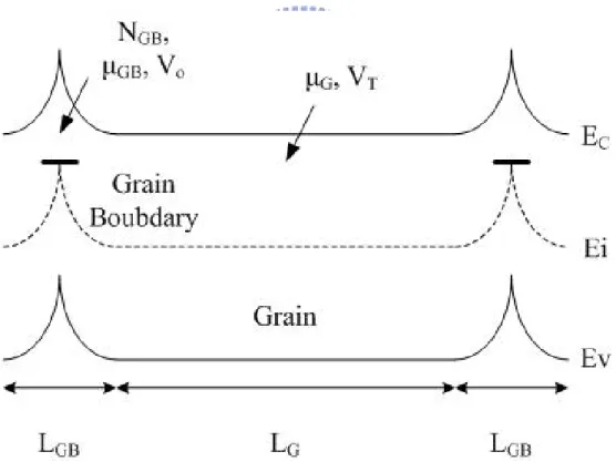
Fig.2-3 (a) Model for the crystal structure of polysilicon films, (b) The charge distribution within the crystallite and at the grain boundary, (c) The energy band structure of the polysilicon crystallites
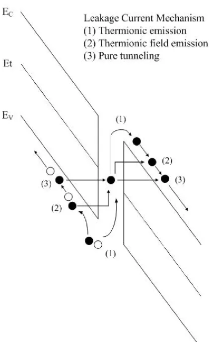
Fig.2-4 Three possible mechanisms of leakage current in poly-Si TFTs, including thermionic emission, thermionic field emission and pure tunneling
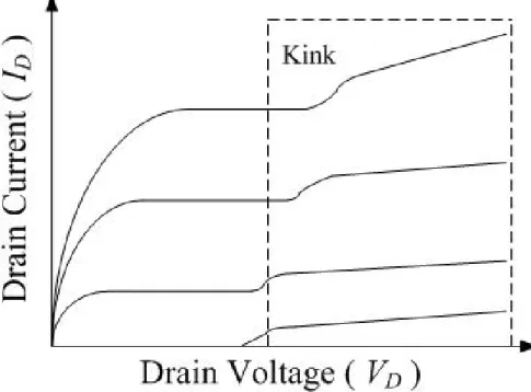
Fig.2-5 The kink effect in the output characteristics of an n-channel SOI MOSFET Fig.2-6 ID–VGS curves of an FG device when there is no charge stored in the FG
and when a negative charge Q is stored in the FG Fig.2-7 The procedure of channel hot electrons injection (CHEI)
Fig.2-8 A schematic energy band diagram describing the three processes involved in electron injection
Fig.2-9 Fourth approaches to programming methods
Fig.2-10 The procedure of band to band hot electron injection Fig.2-11 The procedure of band to band hot hole injection Fig.2-12 The procedure of hot hole injection
Fig.2-13 The procedure of channel initiated secondary electron injection (CHISEL) Fig.2-14 The band-diagram of channel initiated secondary electron injection
(CHISEL)
Fig.2-15 Bandgap diagram of a SONOS device in the excess electron state, showing retention loss mechanisms: trap-to-band tunneling (T-B), trap-to-trap tunneling (T-T), band-to-trap tunneling (B-T), thermal excitation (TE) and Poole–Frenkel emission (PF)
Fig.2-16 The procedure and band diagram for numerous program/erase circles Fig.2-17 Anomalous stress induced leakage current (SILC) modeling. The leakage is
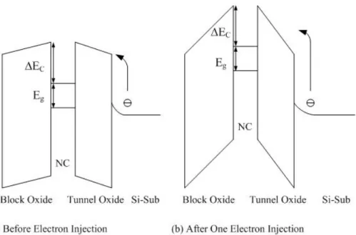
caused by a cluster of positive charge generated in the oxide during erase Fig.2-18 The illustration of the band diagram for coulomb blockade effect (a) before
electron injection, and (b) after one electron injection
Chapter 3
Fig.3-1 The cross-section of F-ions incorporated poly-Si TFTs structure
poly-Si TFTs with F ions implantation dosage of 5×1013 cm-2, (W/L=10um/10um)
Fig.3-3 Output characteristics (ID-VD) of the standard and the fluorine-implanted poly-Si TFTs with F ions implantation dosage of 5×1013cm-2, (W/L=10um/10um)
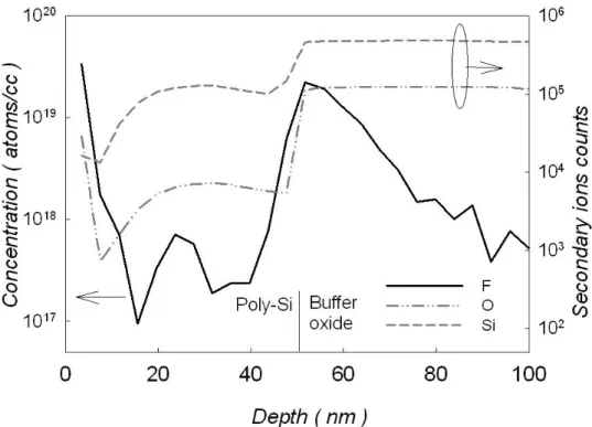
Fig.3-4 The activation energy (EA) of the standard and the fluorine-implanted poly-Si TFTs with F ions implantation dosage of 5×1013 cm-2 at VD=5 V Fig.3-5 Secondary ions mass spectroscope (SIMS) analysis of fluorine-implanted
a-Si film with dosage of 5×1013cm-2 after solid phase recrystallization process
Fig.3-6 The threshold voltage variation (∆VTH) versus stress duration for the standard and the fluorine-implanted poly-Si TFTs with F ions implantation dosage of 5×1013cm-2
Fig.3-7 The on-current variation (∆ION /ION) verse stress time for the standard and the fluorine-implanted poly-Si TFTs with implantation dosage of 5×1013cm-2
Fig.3-8 The subthreshold swing variation (∆S.S) verse versus stress duration for the standard and the fluorine-implanted poly-Si TFTs with F ions implantation dosage of 5×1013cm-2
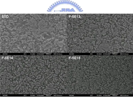
Fig.3-9 The transfer characteristics (ID-VG) of the standard and the fluorine-implanted poly-Si TFTs with various F ions implantation dosages. Fig.3-10 Scanning electron microscopy (SEM) images of the poly-Si film with and
without fluorine ion implantation
Chapter 4
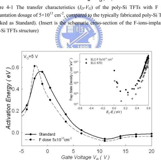
Fig.4-1 The transfer characteristics (ID-VG) of the poly-Si TFTs with F ionsimplantation dosageof 5×1013cm-2, compared to the typically fabricated poly-Si TFTs (marked as Standard). (Insert is the schematic cross-section of the F-ions-implanted poly-Si TFTs structure)
Fig.4-2 The activation energy (EA) of the poly-Si TFTs with and without F ions implantation, as a function of gate voltage.(Drain voltage VD applied at 5V). The insert shows the distribution of trap state density in the poly-Si bandgap
Fig.4-3 Secondary ion mass spectrometer (SIMS) analysis of fluorine in the F-implanted poly-Si film after excimer laser crystallization process Fig.4-4 The threshold voltage variation (∆VTH) as a function of stress time, for the
standard poly-Si TFTs and F-implanted poly-Si TFTs with ion dosage of 5×1013cm-2
Fig.4-5 The on-current variation (∆ION /ION) as a function of stress time for the standard poly-Si TFTs and F- implanted poly-Si TFTs with ion dosage of 5×1013cm-2
Fig.4-6 The subthreshold swing variation (∆S.S) as a function of stress time for the standard poly-Si TFTs and F-implanted poly-Si TFTs with ion dosage of 5×1013cm-2
Fig.4-7 The transfer characteristics (ID-VG) for F-implanted poly-Si TFTs with various ion implantation dosages, compared to the standard poly-Si TFTs (Drain voltage VD applied at 0.1V)
Fig.4-8 Scanning electron microscopy (SEM) images of the standard and the F-implanted poly-Si films
Chapter 5
Fig.5-1 (a)The cross-section of F-ions incorporated poly-Si TFTs, (b)The secondary ions mass spectroscope (SIMS) analysis of F ions in poly-Si channel after SPC, (c)The secondary ions mass spectroscope (SIMS) analysis of F ions in poly-Si channel after ELC
Fig.5-2 The transfer characteristics (ID-VG) of the poly-Si TFTs for F ions implantation dosage of 5×1013cm-2 and standard
Fig.5-3 (a)The activation energy (EA) of the poly-Si TFTs (SPC) for F ions implantation dosage of 5×1013 cm-2 and standard at VD=5 V. (b)The activation energy (EA) of the poly-Si TFTs (ELC) for F ions implantation dosage of 5×1013 cm-2 and standard at VD=5 V
Fig.5-4 (a)The trap state distribution in the bandgap of the poly-Si TFTs (SPC) for F ions implantation dosage of 5×1013 cm-2. (b) The trap state distribution in the bandgap of the poly-Si TFTs (ELC) for F ions implantation dosage of 5×1013cm-2
Fig.5-5 The threshold voltage variation (∆VTH) verse stress time for standard poly-Si TFTs and F-ions-implanted poly-Si TFTs for dosage of 5×1013cm-2 Fig.5-6 The on current variation (∆ION /ION) verse stress time for standard poly-Si
TFTs and F-ions-implanted poly-Si TFTs for dosage of 5×1013cm-2
Fig.5-7 The subthreshold swing variation (∆S.S) verse stress time for standard poly-Si TFTs and F-ions-implanted poly-Si TFTs for dosage of 5×1013cm-2
Chapter 6
Fig.6-1 The device cross-section for the poly-Si TFTs with all layers
Fig.6-2 Fourier transform infrared (FTIR) spectra of FSG film and TEOS film between 2000cm-1 and 400cm-1
Fig.6-3 Comparison of transfer characteristics (ID-VG) for poly-Si TFTs with FSG spacer and TEOS spacer operated at VD= 0.1 V (W/L =10um/5um)
Fig.6-4 Comparison of output characteristics (ID-VD) for poly-Si TFTs with FSG spacer and TEOS spacer, W/L=10um/5um, VG - VTH = 0, 1, 2, 3, 4 V. The threshold voltages of poly-Si TFTs for FSG spacer and TEOS spacer are 7.61V and 7.29V, respectively
Fig.6-5 The variation of transfer characteristics (ID-VG) and transconductance (Gm) characteristics after DC bias stress for poly-Si TFTs with (a)TEOS oxide, and (b)FSG spacer, respectively
Fig.6-6 Comparison of threshold voltage variation (∆VTH) characteristics for poly-Si TFTs with FSG spacer and TEOS spacer, operated at VD=0.1V (W/L=10um/3um)
Chapter 7
Fig.7-1 The process flow proposed in this work. (a) Oxidized a-Si layer as blocking oxide, (b) Directly oxidized SiGeN layer as locking oxide
Fig.7-2 (a)The capacitance-voltage (C-V) hysteresis of the MOIOS structure. The electrical C-V measurements are performed by bidirectional voltage sweeping (1) from 10V~(-10) V and (-10)V~10V ;(2) from 3V~(-3)V and (-3)V~3V: (b)The current density measurement by voltage sweeping from (1) 0V ~ 10V and (2) 0V~ (-10)V
Fig.7-3 (a)The capacitance-voltage (C-V) hysteresis of the MOIOS structure. The electrical C-V measurements are performed by bidirectional voltage sweeping from(I) 3V~(-3)V and (-3)V~3V, (II) 5V~(-5)V and (-5)V~5V, (III) 7V~(-7)V and (-7)V~ 7V, (b)The current density measurement by voltage sweeping from (1) 0V~10V and (2) 0V~(-10)V
Fig.7-4 (a)Raman spectra of the SiGeN with a top capping a-Si layer, before and after thermal oxidation process; (b)Raman spectra of the SiGeN, before and after thermal oxidation process
Fig.7-5 Transmission electron microscopy (TEM) analysis of thermal oxidized SiGeN layer (a)with oxidized a-Si layer as blocking oxide, (b)with directly oxidized SiGeN layer as blocking oxide.
Fig.7-6 (a)The threshold voltage shift (∆VTH) versus different periods of time, (b)The endurance characteristics after different write/erase cycles of Ge nanocrystals nonvolatile memory with oxidized a-Si as blocking oxide Fig.7-7 (a)The retention characteristics and (b) The endurance characteristics of
stacked structure with Ge embedded in SiON as charge trapping layer and oxidized SiGeN as blocking oxide
Chapter 8
Fig.8-1 The capacitance-voltage (C-V) hysteresis of the MOIOS structure for SiON as charge trap center. The electrical C-V measurements are performed by bidirectional voltage sweeping from (1) from 7V~(-7)V and (-7)V~7V; (2) from 5V~(-5)V and (-5)V~5V. The insert is the stacked structure for charge trapping center for SiON layer
Fig.8-2 The capacitance-voltage (C-V) hysteresis of the MOIOS structure for Ge nanocrystal embedded in SiO2 layer as charge trap center. The electrical C-V measurements are performed by bidirectional voltage sweeping from 5V~(-5)V and (-5)V~5V. The insert is the stacked structure for charge trapping center for Ge nanocrystal embedded in SiO2 layer
Fig.8-3 The capacitance-voltage (C-V) hysteresis of the MOIOS structure for Ge nanocrystal embedded in SiON layer as charge trap center. The electrical C-V measurements are performed by bidirectional voltage sweeping from 5V~(-5)V and (-5)V~5V. The insert is the stacked structure for charge trapping center for Ge nanocrystal embedded in SiON layer
Fig.8-4 The band diagrams for charge trapping center for (a) SiON layer, (b) Ge nanocrystal embedded in SiO2 layer, and (c) Ge nanocrystal embedded in SiON layer, respectively
Chapter 9
Fig.9-1 The capacitance-voltage (C-V) hysteresis of the MOIOS structure for (a) condition A (dry oxidation 30min), (b)condition B (dry oxidation 45min), respectively
Fig.9-2 The capacitance-voltage (C-V) hysteresis of the MOIOS structure for condition C (dry oxidation 60min). The insert is the transmission electron microscopy (TEM) analysis
Fig.9-3 The capacitance-voltage (C-V) hysteresis of the MOIOS structure for condition D (dry oxidation 30min plus steam treatment 3min). The insert is the transmission electron microscopy (TEM) analysis
Fig.9-4 The current-voltage (I-V) hysteresis of the MOIOS structure for condition A, B, C and D, respectively
Fig.9-5 The Auger electron spectroscopy (AES) analysis of (a) stacked structure, (b) oxidized stacked structure for dry oxidation 30min
Fig.9-6 (a)The Auger electron spectroscopy (AES) analysis of stacked structure for 60min dry oxidation, (b) The transmission electron microscopy (TEM) analysis of stacked structure for 60min dry oxidation
30min dry oxidation plus 3min steam treatment, (b) The transmission electron microscopy (TEM) analysis of stacked structure for 30min dry oxidation plus 3min steam treatment
Fig.9-8 The comparison of the Raman spectra of stacked structure for dry oxidation 30min and 45min
Fig.9-9 The comparison of the Raman spectra of oxidized SiGeN layer for 30min dry oxidation and 30min dry oxidation plus 3min steam treatment, respectively
Fig.9-10 The comparison of the Raman spectra of oxidized SiGeN layer for 60min dry oxidation and 60min dry oxidation plus 3min steam treatment, respectively
Chapter 10
Fig.10-1 The capacitance-voltage (C-V) hysteresis of the MOIOS structure for (a) condition A (dry oxidation 30min), (b)condition B (dry oxidation 45min), respectively
Fig.10-2 The capacitance-voltage (C-V) hysteresis of the MOIOS structure for (a) condition C (dry oxidation 60min) and condition D (dry oxidation 30min plus steam treatment 3min), respectively
Fig.10-3 The current-voltage (I-V) hysteresis of the MOIOS structure for condition A, B, C and D, respectively
Fig.10-4 (a)The Auger electron spectroscopy (AES) analysis of stacked structure, (b) The TEM analysis of stacked structure
Fig.10-5 (a)The Auger electron spectroscopy (AES) analysis of stacked structure for 60min dry oxidation, (b) The TEM analysis of stacked structure for 60min dry oxidation
Fig.10-6 (a)The Auger electron spectroscopy (AES) analysis of stacked structure for 30min dry oxidation plus 3min steam treatment, (b) The TEM analysis of stacked structure for 30min dry oxidation plus 3min steam treatment Fig.10-7 The process flow proposed in this work for 60min dry oxidation, and
30min dry oxidation plus 3min steam treatment
Fig.10-8 The Raman spectra of oxidized SiGeN layer for (a) 30min, and (b) 60min dry oxidation, respectively
Fig.10-9 The Raman spectra of oxidized SiGeN layer for 30min dry oxidation, and 30min dry oxidation plus 3min steam treatment, respectively
Fig.10-10 The Raman spectra of oxidized SiGeN layer for 60min dry oxidation, and 60min dry oxidation plus 3min steam treatment, respectively
Chapter 1
Introduction
1.1 Overview of Poly-silicon Thin-Film Transistor Technology
In recent years, polycrystalline silicon thin film transistors (poly-Si TFTs) have been drawn much attention because of their widely applications on active matrix liquid crystal displays (AMLCDs) [1.1], and organic light-emitting displays (OLEDs) [1.2]. Except large area displays, poly-Si TFTs also have been applied into some memory devices such as dynamic random access memories (DRAMs) [1.3], static random access memories (SRAMs) [1.4], electrical programming read only memories (EPROM) [1.5], electrical erasable programming read only memories (EEPROMs) [1.6], linear image sensors [1.7], thermal printer heads [1.8], photo-detector amplifier [1.9], scanner [1.10], neutral networks [1.10]. Lately, some superior performances of poly-Si TFTs also have been reported by scaling down device dimension or utilizing novel crystallization technologies to enhance poly-Si film quality [1.11-1.12]. This provides the opportunity of using poly-Si TFTs into three-dimension (3-D) integrated circuit fabrication. Of course, the application in AMLCDs is the primary trend, leading to rapid developing of poly-Si TFT technology.
The major attraction of applying poly-Si TFTs in AMLCDs lies in the greatly improved carrier mobility in poly-Si film and the capability of integrating the pixel switching elements and the capability to integrate panel array and peripheral driving circuit on the same substrates [1.13-1.15]. In poly-Si film, carrier mobility larger than 15 cm2/Vs can be easily achieved, that is enough to used as peripheral driving circuit including n- and p-channel devices. This enables the fabrication of peripheral circuit and TFT array on the same glass substrate, bring the era of system-on-glass (SOG)
technology. The process complexity can be greatly simplified to lower the cost. In addition, the mobility of poly-Si TFTs is much better than that of amorphous ones, the dimension of the poly-Si TFTs can be made smaller compared to that of amorphous Si TFTs for high density, high resolution AMLCDs, and the aperture ratio in TFT array can be significantly improved by using poly-Si TFTs as pixel switching elements. This is because that the device channel width can be scaled down while meeting the same pixel driving requirements as in amorphous silicon thin film transistors (a-Si TFTs) AMLCDs.
For making high performance poly-Si TFTs, low-temperature technology is required for the realization of commercial flat-panel displays (FPD) on inexpensive glass substrate, since the maximum process temperature is limited to less than 600°C [1.16]. There three major low-temperature a-Si crystallization methods to achieve high performance poly-Si thin film, solid phase crystallization (SPC), excimer laser crystallization (ELC), and metal-induced lateral crystallization (MILC). Typical fabrication of poly-Si TFTs include the deposition of amorphous silicon (a-Si) followed by long time furnace crystallization (> 20 h). Such a crystallization method is called solid phase crystallization (SPC). The SPC method has the advantage of good uniformity and smoother interface. However, the throughput is limited by the long crystallization time. In recent years, excimer laser crystallization (ELC) has been applied to crystallize the a-Si to poly-Si with lower temperature (substrate room temperature) compared to SPC. In addition, the ELC does not require a long time crystallization process, and a larger grain size compared to that with SPC method is possible with ELC method, which is ideally suited for applications of poly-Si TFTs. However, the roughness and uniformity of poly-Si films after ELC method is an important issue and it may degrade the electrical properties if ELC is not carefully controlled. In the last few years, several articles have been devoted to study of the
growth mechanism of metal-induced-lateral-crystallization (MILC). Earlier observation of Ni induced crystallization of a-Si revealed that the onset temperature for crystallization of a-Si was significantly reduced in presence of NiSi2 precipitates and crystallization occurred at around 5000C. The NiSi2 precipitates acts as a good nucleus of Si, which has similar crystalline structure (the fluorite type, CaF2) and a small lattice mismatch of 0.4% with Si. In the case of Ni induced crystallization, the growth of crystallites depends strongly on the migration of NiSi2 precipitates, and the driving force for the migration of NiSi2 precipitates is the reduction in free energy associated with the transformation of metastable a-Si to stable c-Si.
However, some problems still exist in applying poly-Si TFTs on large-area displays. In comparison with single-crystalline silicon, poly-Si is rich in grain boundary defects as well as intra-grain defects, and the electrical activity of the charge-trapping centers profoundly affects the electrical characteristics of poly-Si TFTs. Large amount of defects serving as trap states locate in the disordered grain boundary regions to degrade the ON current seriously [1.17]. Moreover, the relatively large leakage current is one of the most important issues of conventional poly-Si TFTs under OFF-state operation [1.18-1.19]. In most application, a low-cost substrate is essential and therefore a low temperature process (i.e., <650°C) compatible with glass substrates is developed [1.20]. In summary, it is expected that the poly-Si TFTs will becomes more important in future technologies, especially when the 3-D circuit integration era is coming. More researches studying the related new technologies and the underlying mechanisms in poly-Si devices with shrinking dimensions are therefore worthy to be indulged in.
1.1.1 Defects in Poly-Si Film
intragranular defects exist in the film. The dangling bonds in grain boundaries will affect device characteristics seriously because they act as trapping centers to trap carriers. Carriers trapped by these low energy traps can no longer contribute to conduction, which results in the formation of local depletion region and potential barriers in these grain boundaries. Thus, the typical characteristics such as threshold voltage (VTH), subthreshold swing (S.S), on current (ION), field effect mobility (µFE) and transconductance (Gm) of TFTs are inferior to those of devices fabricated on single crystal silicon film. As for the leakage current, it is well known that the leakage current increase with the drain voltage and gate voltage. The dominant mechanism of the leakage current is field emission via grain boundary traps due to the high electric field near the drain junction [1.21-1.24].
To overcome this inherent disadvantage of poly-Si film, many researches have been focused on modifying or eliminating these grain boundary traps. Traps are associated with dangling bonds arising from lattice discontinuities between different oriented grains or at the Si/SiO2 interface. The most useful method so far to remove traps is to passivate these dangling bonds, such as hydrogen plasma treatment has been utilized for the passivation [1.25-1.26], but it is difficult to control the hydrogen concentration in the TFT. The Si-H bonds may be broken under hot-carrier stress [1.27-1.28], leading to degradation of electrical characteristics after a long-term operation time. As the number of trapped carrier decreases, the potential barriers in grain boundaries decrease. And the leakage current decreases because of the fewer trap density near the drain region.
1.1.2 Motivation
To meet the requirement of higher circuit density and higher speed, it is necessary to improve the performance of the poly-Si TFTs. Although poly-Si TFTs
have many superior advantages, the presence of a large number of grain boundaries in poly-Si TFTs contributes a large density of defects which cause the localized states in the energy gap and degrade performance. Hence, the reliability issue is one of the most constraints toward the applications. In the preview research, enlarging the grain size and passivating the defects at the grain boundary were widely used methods to reduce the trap states in the grain boundary. Generally, hydrogen plasma treatment has been utilized for the passivation, but it is difficult to control the hydrogen concentration in the TFTs. In recent years, fluorine ion implantation was applied to improve the electrical characteristics by eliminating the defects in the grain boundary [1.29-1.30]. It is found that the fluorine atoms piled up at the interface between the poly-Si and oxide to break the stress induced strained bonds to form stronger Si-F bonds, leading to local stress relaxation and thus decreasing the tail state density [1.31]. The fluorine atoms can also be the terminator of dangling bonding in poly-Si. Hence, the TFT with fluorine implantation has the superior electrical characteristics than conventional poly-Si TFTs. However, it needs additional oxide layer deposition and additional thermal annealing. The extra process steps will increase the difficulty for the fabrication of poly-Si TFTs. In this work, the electrical characteristics behaviors of poly-Si TFTs by various fluorine ion implantation dosages were investigated. In addition, there was no any pad oxide deposited firstly before thermal annealing. Hence, it also needed no additional thermal annealing step. Furthermore, it is known that one of the degradation is caused by the energetic electrons generated by impact ionization near the drain. By introducing the fluorinated silica glass (FSG) spacer technique, the stronger Si-F bonds passivate the interface of the drain which is the largest lateral electric field region location for light doped drain (LDD) structure. This method needs not additional process step and also can achieve the improvement of reliability. The electrical characteristics, including I-V measurement and DC bias
stress reliability, were reported in this study. In addition, the material analysis such as secondary ion mass spectrometry (SIMS), and scanned electron microscope (SEM) were also discussed.
1.2 Overview of Nonvolatile Memory
In 1967, D. Kahng and S. M. Sze invented the floating-gate (FG) nonvolatile semiconductor memory (or flash memory) at Bell Labs [1.32]. To date, the flash memory device continues to be the most prevailing nonvolatile-memory implementation, and is widely used in both standalone and embedded memories. The invention of flash memory creates a huge industry of portable electronic devices such as cellular phones, digital cameras, digital voice recorders, MP3 walkman, personal data assistants to compact smart cards, USB flash personal disc etc.
Although a huge commercial success, conventional FG devices have their limitations. Two of the most prominent limitations are: (1) the limited potential for continued scaling of the device structure. This scaling limitation stems from the extreme requirements put on the tunnel oxide layer. The tunnel oxide must be thin enough to allow quick and efficient charge transport to and from FG. On the other hand, the tunnel oxide needs to provide superior isolation under retention, endurance, and disturbed conditions in order to maintain information integrity over periods of up to a decade. When the tunnel oxide is thinner for operation speed consideration, the retention characteristics may be degraded. And when the tunnel oxide is made thicker to take the isolation into account, the speed of the operation will be slower. Therefore, for mass production, there is a trade-off between speed and reliability for the optimal tunnel oxide thickness. (2) The quality and strength of tunnel oxide (or tunnel dielectric) after plenty of program/erase cycles. Once a leaky path has been created in
tunnel oxide, all the charges stored in the floating gate will be lost. Therefore, two suggestions, poly-Si/oxide/nitride/oxide/Si (SONOS) [1.33-1.35] and nanocrystal nonvolatile memory devices [1.36-1.38], are proposed to overcome this oxide quality limit of the conventional FG structure. These technologies replace the floating gate structure with a great number of charge-storage nodes in the dielectric or in the nanocrystal. Unlike the floating gate, stored charges in isolated nodes cannot easily redistribute amongst themselves and the local leaky path will not cause the fatal loss of information for the nanocrystal nonvolatile memory device. This effectively prevents the leakage of all the stored charges out of the floating gate.
1.2.1 SONOS nonvolatile memory devices
poly-Si/oxide/nitride/oxide/silicon (SONOS) nonvolatile memory devices structure, the charge storage elements in SONOS memory are the charge traps distributed throughout the volume of the Si3N4 layer. A typical trap has a density of the order 1018-1019 cm-3 according to Yang et al [1.39] and stores both electrons and holes (positive charges) injected from the channel.
The nitride-based memory devices were extensively studied in the early 70s after the first metal-gate nitride device metal/nitride/oxide/silicon (MNOS) was reported in 1967 by Wegener et al [1.40]. Initial device structures in the early 1970s were p-channel metal-nitride-oxide-silicon (MNOS) structures with aluminum gate electrodes and thick (45nm) silicon nitride charge storage layers. Write/erase voltages were typically 25-30 V. In the late 1970s and early 1980s, scaling moved to n-channel silicon-nitride-oxide-silicon (SNOS) devices with write/erase voltages of 14-18 V. In the late 1980s and early 1990s, n- and p-channel SONOS devices emerged with write/erase voltages of 5-12 V. In the SONOS device, an oxide layer is introduced
between the gate and the nitride region. Thus, it forms the SiO2/Si3N4/SiO2 (ONO) gate dielectric stack instead of capping the nitride layer with just a metal or semiconductor gate. The purpose of the top blocking oxide is to reduce the charge injection from the control gate into the nitride layer, limiting the memory window of both MNOS and SNOS devices.
During programming, the control gate is biased positively so that electrons from the channel can tunnel across the SiO2 into the nitride layer. Some electrons will continue to move through the nitride layer then across the control oxide finally into the control gate. The remaining trapped charges in the nitride layer provide the electrostatic screening of the channel from the control gate. Therefore, there is a threshold voltage (VTH) shift resulting from trapped charges in nitride and because of that SONOS can be used as a memory device just like conventional floating gate devices.
1.2.2 Nanocrystal nonvolatile memory devices
Nanocrystal nonvolatile memories are one particular implementation of storing charges by dielectric-surrounded nanodots, and were first introduced in the early 1990s by IBM researchers who proposed flash memory with a granular floating gate made from silicon nanocrystals [1.41], In a nanocrystal nonvolatile semiconductor memory (NVSM) device, charge is not stored on a continuous FG poly-Si layer, but instead on a layer of discrete, mutually isolated, crystalline nanocrystals or dots. Each dot will typically store only a handful of electrons; collectively the charges stored in these dots control the channel conductivity of the memory transistor.
As compared to conventional stacked gate NVSM devices, nanocrystal charge storage offers several advantages, the main one being the potential to use thinner
tunnel oxide without sacrificing nonvolatility. This is a quite attractive proposition since reducing the tunnel oxide thickness is a key to lowering operating voltages and/or increasing operating speeds. This claim of improved scalability results not only from the distributed nature of the charge storage, which makes the storage more robust and fault-tolerant, but also from the beneficial effects of Coulomb blockade [1.42]. Quantum confinement effects (bandgap widening; energy quantization) can be exploited in sufficiently small nanocrystal geometries (sub-3 nm dot diameter) to further enhance the memory’s performance.
Due to the less drain to FG coupling, nanocrystal memories suffer less from drain induced barrier lowering (DIBL). One way to exploit this advantage is to use a higher drain bias during the read operation, thus improving memory access time. Of particular importance is the low capacitive coupling between the external control gate and the nanocrystal charge storage layer. This does not only results in higher operating voltages, thus offsetting the benefits of the thinner tunnel oxide, but also removes an important design parameter (the coupling ratio) typically used to optimize the performance and reliability tradeoff.
Unlike volume distributed charge traps (ex: nitride in SONOS NVM), nanocrystals be deposited in a two-dimensional 2-D) layer at a fixed distance from the channel separated by a thin tunnel oxide. By limiting nanocrystals deposition to just one layer and adjusting the thickness of the top blocking dielectric, charge leakages to the control gate from the storage nodes can be effectively prevented.
1.2.3 Motivation
The Semiconductor Industry Association (SIA) International Technology Roadmap for Semiconductors (ITRS) indicates the difficult challenge, beyond the
year 2005, for nonvolatile semiconductor memories is to achieve reliable, low-power, low-voltage performance [1.43]. For nonvolatile flash memories, two limitations encountered at the present time are: (1) the limited potential for continued scaling of the device structure. This scaling limitation stems from the extreme requirements put on the tunnel oxide layer. In order to get balance between program/erase speed and retention time, there is a trade-off between speed and reliability to get the optimal tunnel oxide thickness; (2) the quality and strength of tunnel oxide (or tunnel dielectric) after plenty of program/erase cycles. Once a leaky path has been created in tunnel oxide, all the charges stored in the floating gate will be lost. Therefore, two suggestions, the SONOS and the nanocrystal nonvolatile memory devices, are proposed to overcome this oxide quality limit of the conventional FG structure. These technologies replace the floating gate structure with a great number of charge-storage nodes in the dielectric or in the nanocrystal. Unlike the floating gate, the local leaky path will not cause the fatal loss of information for the nanocrystal nonvolatile memory device. This effectively prevents the leakage of all the stored charges out of the floating gate.
In this thesis, a combination of SONOS and nanocrystal nonvolatile memory devices is proposed. A SiGeN film is introduced to replace the nitride film in SONOS structure. After several different thermal processes, Ge in the SiGeN film will be segregated to form Ge nanodots embedded in the SiNx (or SiON) film. Because there are two charge-storage node sources, the nodes in Ge nanodots and in SiNx dielectric film, comparing to SONOS and Ge nanocystal NVMs, a larger memory window can be obtained. When a memory device has a larger memory window, it is easier to meet the requirement of retention of 10 years. And, hope to solve the two limitations mentioned above.
1.3 Thesis Organization
In this thesis, novel methods were proposed to improve the electrical characteristics of low temperature polycrystalline silicon thin film transistors (LTPS). In addition, the advanced nonvolatile memory devices were also fabricated and investigated for solving the problem of conventional nonvolatile memory. In chapter2, the transport properties and trap model of the poly-Si TFTs were introduced. Furthermore, the program/erase methods for memory device were also discussed. Also, the models of the reliability test were also investigated.
In chaprter3, fluorine ions implantation technology was applied for poly-Si TFTs fabrication. Before solid phase crystallization (SPC), fluorine ions were implanted to amorphous silicon (a-Si). The surface-oxidized a-Si is the driving force for fluorine ions segregating. The obvious fluorine concentration was observed at the surface of poly-Si and the interface between poly-Si and buffer oxide. The performance of fluorine-ions-implanted poly-Si TFTs was enhanced, due to the trap state density elimination.
In chapter4, the fluorine-ions-implanted poly-Si TFTs using excimer laser crystallization (ELC) method was also fabricated and investigated. The improvement of electrical characteristics of fluorine-ions-implanted poly-Si TFTs resulted from the pssivation of poly-Si. In addition, the segregated fluorine ions at the interface of poly-Si and buffer oxide reduces the mechanical stress resulted from the rapid crystallization.
In chaper5, the electrical characteristics and the electrical reliability of fluorine-ions-implanted poly-Si TFTs were investigated. The stronger Si-F bonds, replacing the Si-Si and Si-H bonds in the poly-Si, can resist the current impact. Hence, the reliability of fluorine-ions-implanted poly-Si TFTs is improved. The obvious enhancement of the reliability was found for using ELC method; due to the lower trap
state density was obtained. Furthermore, the strong Si-F bonds is suitable to resist the higher current impact due to the poly-Si TFTs using ELC method.
In chapter6, fluorinated silica glass (FSG) was used for the application of spacer on poly-Si TFTs. The presence of FSG spacers can effectively reduce the lateral electrical field near the drain side of poly-Si TFT device, and strongly passivate Si dangling bonds at the grain boundaries. The significant enhancement in electrical performance suppresses serious kink effect, and improves electrical reliability of poly-Si TFTs effectively.
In chapter7, a large memory window is observed due to isolated Ge nanocrystals in the silicon-oxygen-nitride (SiON) gate stack layer. The Ge nanocrystals were nucleated after high temperature oxidized silicon-germanium-nitride (SiGeN) layer. Also, the manufacture technology using the sequent high-temperature oxidation of the amorphous silicon (a-Si) layer and directly oxidation of the SiGeN layer acting as the blocking oxide is proposed to enhance the performance of nonvolatile memory devices, respectively.
In chapter8, the formation of Ge nanocrystals embedded in SiON is proposed for charge storage elements in this work. Compared to the control samples of Ge nanocrystals /SiO2 /Si structure and SiON/Si stack memory, the proposed Ge nanocrystals/SiON/Si memory obtained superior memory window, even larger than the summation of the typical both. It is considered that the extra interface trap states between Ge and SiON film was generated as Ge nanocrystals were embedded in SiON layer.
In chapter9, the Ge nanocrystal formation by oxidizing SiGeN with distributed charge storage elements is proposed in this work. The manufacture technology using the sequent high-temperature oxidation of a-Si layer acting as the blocking oxide. The longer duration of dry oxidation causes obvious Ge nanocrystals formation. Also,
simple steam treatment improves the quality of blocking oxide and reduces the thermal budget of fabrication. Furthermore, overall oxidation by steam treatment causes initial Ge nanocrystal to become germanium oxide which is also a charge trapping center.
In chapter10, the Ge nanocrystal formation by oxidizing SiGeN with distributed charge storage elements is proposed in this work. The manufacture technology using the sequent high-temperature oxidation of SiGeN layer acting as the blocking oxide. Simple steam treatment improves the quality of blocking oxide. However, the Ge nanocrystals were formed far from the tunneling oxide which is obviously different from the long dry oxidation condition for quickly oxidation. In addition, the Ge nanocrystals were also oxidized after steam treatment.
Finally, conclusions and future work as well as recommendation for further research are given in chapter11 and chapter12, respectively.
Chapter 2
Poly-Si
TFTs
Conduction
Mechanism
and
Nonvolatile Memory Basics Principles
2.1 Poly-Si TFTs Transportation Mechanisms
The device characteristics of poly-Si TFTs are strongly influenced by the grain structure in poly-Si film. Even though the inversion channel region is also induced by the gate voltage as in MOSFETs, the existence of grain structure in channel layer bring large differences in carrier transport phenomenon. A schematic MOSFET cross section, showing the axes of coordinates and the bias voltages at the four terminals, for the drain-current model is as shown in Figure 2-1. Many researches studying the electrical properties and the carrier transport in poly-Si TFTs have been reported. A simple grain boundary-trapping model has been described by many authors in details [2.1-2.3]. In this model, it is assumed that the poly-Si material is composed of a linear chain of identical crystallite having a grain size Lg and the grain boundary trap density Nt (cm-3). The charge trapped at grain boundaries is compensated by oppositely charged depletion regions surrounding the grain boundaries. From Poisson’s equation, the charge in the depletion regions causes curvature in the energy bands, leading to potential barriers that impede the movement of any remaining free carriers from one grain to another. When the dopant/carrier density n (or ND) (cm-3) is small, the poly-Si grains will be fully depleted. The width of the grain boundary depletion region xd extends to be Lg/2 on each side of the boundary, and the voltage barrier height VB can be expressed as
Fully depleted: S g d S B qnL x qn V ε ε 8 2 2 2 = = (2-1)
As the dopant/carrier concentration is increased, more carriers are trapped at the grain boundary. The curvature of the energy band and the height of potential barrier increase, making carrier transport form one grain to another more difficult. When the dopant/carrier density increases to exceed a critical value N* = Nt / Lg, the poly-Si grains turn to be partially depleted and excess free carriers start to spear inside the grain region. The depletion width and the barrier height can be expressed as
Partially depleted: n N x t d 2 = (2-2) n qN n N qn V s t t s B ε ε 8 ) 2 ( 2 2 2 = = (2-3)
The depletion width and the barrier hight turn to decrease with increasing dopant/carrier density, leading to improved conductivity in carrier transport.
The carrier transport in fully depleted poly-Si film can be described by the thermionic emission over the barrier. Its’ current density can be written as [2.4]
)] ( exp[ B a c V V kT q qnv J = − − (2-4)
where n is the free-carrier density, vc is the collection velocity (vc = kT/2πm∗ ), VB
is the barrier height without applied bias, and Va is the applied average bias across the
one grain boundary region. For small-applied biases, the applied voltage divided approximately uniformly between the two sides of a grain boundary. Therefore, the barrier in the forward-bias direction decreases by an amount of Va/2. In the
reserve-bias direction, the barrier increases by the same amount. The current density in these two directions then can be expressed as
)] 2 1 ( exp[ B a c F V V kT q qnv J = ⋅ − − (2-5) )] 2 1 ( exp[ B a c R V V kT q qnv J = ⋅ − + (2-6)
Thus the net current density is then given by ) 2 sinh( ) exp( 2 kT qV kT qV qnv J B a c − = (2-7) At low applied voltages, the voltage drop across a grain boundary is small compared to the thermal voltage kT/q, thus Eq. (2-7) can be simplified as
)] [exp( 2 ) exp( 2 2 kT qV kT V nv q kT qV kT qV qnv J B a c a B c − = − = (2-8)
the average conductivity σ = J / ξ = JLg / Va , and the effective mobility σ =qnµeff
then the average conductivity can be obtained as
2 exp( ) c g B q nv L qV kT kT σ = − (2-9) ) exp( ) exp( 0 kT qV kT qV kT L qv B B g c eff = − ≡µ − µ (2-10)
where µ0 represents the carrier mobility inside grain regions. It is found that the
conduction in poly-Si is an activated process with activation energy of approximately qVB, which depends on the dopant/carrier concentration and the grain boundary trap
density.
Applying gradual channel approximation to poly-Si TFTs, which assumes that the variation of the electric field in the y-direction (along the channel) is much less than the corresponding variation in the y-direction (perpendicular to the channel), as shown Figure 2-2. The carrier density n per unit area (cm-2) induced by the gate
voltage can be expressed as
ch TH G ox qt ) -V (V C n = (2-11) where
VTH is the threshold voltage,
C
oxis gate oxide capacitance per unit area.
ch D J W t I = ⋅ ⋅ (2-12) ξ µ ⋅ ⋅ ⋅ =n q eff J (2-13) L V L L L V L N V L V D g g D g g D g a = = = =
ξ ; Ng is the grain number (2-14)
Therefore, by replacing Eq. (2-11), (2-13) and (2-14) into Eq. (2-12), the drain current of poly-Si TFT then can be given by
(
)
exp( ) kT qV V V V L W C I B o D TH G ox D= − ⋅ ⋅µ − (2-15)Obviously, this I-V characteristic is very similar to that linear region of MOSFETs, except that the mobility is modified.
2.1.1 Methods of Device Parameter Extraction
In this section, we will introduce the methods of typical parameters extraction such as threshold voltage (Vth), subthreshold slope (S.S), drain current ION /IOFF ratio,
field-effect mobility (µFE), and the trap density (Nt). Determination of the threshold voltage
Many ways are used to determinate the Vth which is the most important
parameter of semiconductor devices. In poly-Si TFTs, the method to determinate the threshold voltage is constant drain current method. The gate voltage at a specific drain current IN value is taken as the threshold voltage. This technique is adopted in most
studies of TFTs. Typically, the threshold current IN = ID / (W/ L) is specified 10 nA for
VD = 0.1V (saturation region) in this thesis.
Determination of the subthreshold slope
the gate control toward channel. And in intrinsic polysilicon TFTs the parameter SS is directly related with the total trap states density NT by the relationship
+ = OX T si C N t q q kT SS 2 1 10 ln (2-16) where
kT is the thermal energy,
tsi is the polysilicon layer thickness.
Thus, the decrease of SS with stressing suggests a decrease in the total trap states density, which includes both bulk and interface traps. The S.S should be independent of drain voltage and gate voltage. However, in reality, S.S might increase with drain voltage due to short-channel effects such as charge sharing, avalanche multiplication, and punchthrough-like effect. The S.S is also related to gate voltage due to undesirable factors such as serial resistance and interface state. In this experiment, the S.S is defined as one-half of the gate voltage required to decrease the threshold current by two orders of magnitude (from 10-8A to 10-10A).
Determination of ION /IOFF Current Ratio
Drain ION /IOFF current ratio is another important factor of TFTs. High ION /IOFF
ratio represents not only large turn-on current but also small off current (leakage current). It affects gray levels (the bright to dark state number) of TFT AMLCD directly.
There are many methods to specify the on and off current. The practical one is to define the maximum current as on current and the minimum leakage current as off current while drain voltage is applied at 5V.
Determination of the field-effect mobility
The field-effect mobility (µFE) is determined from the transconductance (gm) at
TFT can be expressed as ] ) [( G TH D ox FE D V V V L W C I =µ −
(2-17) where W is channel width, L is channel length,
The transconductance is defined as
D FE ox const V G D m V L WC V I g D =
µ
∂ ∂ = = . (2-18)Therefore, the field-effect mobility can be obtained by
gm D ox FE WV C L = µ (2-19)
Modification of effective field-effect mobilityyyy
According Seto model, in uniform small grain poly-Si TFT, the effective field-effect mobility can be expressed [2.5]:
) exp( ) exp( 0 kT qV kT qV kT L qv B B g c eff = − ≡µ − µ
However, in poly-Si films with enlarged grains, the uniform trap distribution model fails to give reliable results due to high nonuniformity of the polycrystalline material. According to Farmakis et al. model, theμeffdepend on the number of grain
boundaries present within the channel of the transistor [2.6]. Figure 2-3 represents the energy band structure of the polysilicon in the neighborhood of the grain boundaries of a n-channel polysilicon TFT along the channel in the linear region of operation (low drain voltage VD). This energy band structure has two resistances RG and RGB
equivalent to the grain region and the grain boundary respectively, both modulated by the gate voltage VG. The grain region is considered to behave as in a bulk MOSFET.
Therefore, considering an average number of n GB’s and n entire grains within the channel, according to the standard MOSFET theory, the total channel resistance Rch