Mid-infrared electroluminescence at room temperature from InAsSb
multi-quantum-well light-emitting diodes
A. Krier,a兲 M. Stone, and Q. D. Zhuang
Department of Physics, Lancaster University, Lancaster LA1 4YB, United Kingdom Po-Wei Liu, G. Tsai, and H. H. Lin
Department of Electrical Engineering, National Taiwan University, Taipei 106, Taiwan and Institute of Electronic Engineering, National Taiwan University, Taipei 106, Taiwan
共Received 24 May 2006; accepted 6 July 2006; published online 30 August 2006兲
Room-temperature electroluminescence is reported from InAsSb multiple-quantum-well light-emitting diodes. The diodes exhibited emission in the mid-infrared peaking near 4m. The spectral dependence on injection current at 4 K was investigated and two transitions were identified, centered at 4.05 and 3.50m, which are associated with the eigenstates of the confined holes inside the quantum well. The use of an Sb predeposition and As flux surface exposure during epitaxial growth was observed to have a major effect on the electroluminescence output. © 2006 American
Institute of Physics. 关DOI:10.1063/1.2339036兴
The development of light sources and detectors for the mid-infrared 共2–5m兲 spectral region continues to be of much academic and technological interest. If suitable opto-electronic components could be made available, one can en-visage a wide variety of applications, including chemical process control, environmental monitoring of atmospheric pollution, noninvasive medical diagnosis, tunable IR spec-troscopy, and free space optical communications. InAs1−xSbx alloys are promising materials for this spectral region; how-ever, strong nonradiative Auger recombination in these ma-terials results in low room-temperature quantum efficiencies in practical devices. One possible solution is to fabricate type II multiple-quantum-well共MQW兲 structures and make use of the two dimensional confinement to suppress Auger recom-bination and improve electroluminescence output.
Previous work in our laboratory using liquid phase epi-taxial growth of InAsSb bulk alloys has resulted in light-emitting diodes共LEDs兲 which operate at 300 K with emis-sion peaking near 4.2m appropriate for CO2detection.1In recent years MQW structures containing InAsSb have been used in the active region of diode lasers grown on GaSb and GaAs substrates by molecular beam epitaxy共MBE兲 or metal-organic vapor phase epitaxy 共MOVPE兲.2,3 By comparison, there have been very few reports of LEDs based on InAsSb MQW exhibiting emission within the 2 – 5m spectral range at room temperature.4 Previously, we have reported on the photoluminescence共PL兲 from InAs1−xSbxquantum dot in the mid-infrared near 4m.5In the present work we report on the observation of electroluminescence 共EL兲 from InAs0.87Sb0.13/ InAs MQW light-emitting diodes grown by MBE.
The InAsSb/ InAs MQW samples for this work were grown on共100兲 p+-InAs substrates using a VG-V80H MBE system. Two cracker cells were used to provide the Sb and As2beams. A thermal effusion K cell was used to provide the In flux. A p+-InAs buffer layer with a thickness of 300 nm was grown at 450 ° C, followed by a ten-period InAsSb/ InAs MQW with 13% Sb composition which was grown at 466 ° C. The thicknesses of the InAsSb well and
InAs barrier were 7 and 24 nm, respectively. Finally, a n+ layer was grown to complete the simple homojunction
p-i-n diode structure. In situ reflection high energy electron
diffraction was used to monitor surface reconstruction. After growth the samples were characterized using double crystal x-ray diffraction and PL or EL spectroscopy to study their structural and optical properties. For EL measurements the as-grown sample was processed into 1 mm diameter mesa-etched LEDs using standard photolithographic techniques. The resulting diodes were mounted onto TO-46 headers for testing and a quasicontinuous current 共50% duty cycle兲 at 1 kHz was used to excite EL in the LEDs. The corresponding low temperature luminescence spectra were measured using a Bentham 0.3 m monochromator and a 77 K InSb photodi-ode to detect the radiation. We investigated the influence of the As and Sb switching sequences employed during MBE growth on the structural properties and also on the resulting EL emission properties.
Figure 1 shows the high resolution x-ray diffraction
a兲Electronic mail: [email protected]
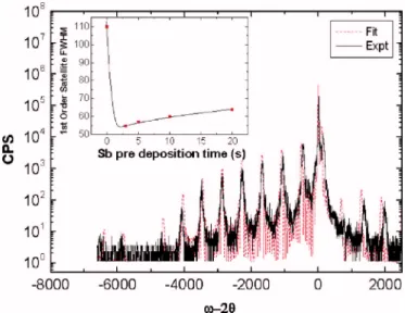
FIG. 1. 共Color online兲 High resolution x-ray diffraction spectra obtained from one of the InAsSb/ InAs MQW samples; solid line—experimental re-sults, dashed line—simulated data. Inset shows FWHM dependence on Sb predeposition time.
APPLIED PHYSICS LETTERS 89, 091110共2006兲
0003-6951/2006/89共9兲/091110/3/$23.00 89, 091110-1 © 2006 American Institute of Physics
spectrum measured from a sample containing ten InAsSb quantum wells. A number of well defined satellite peaks are easily observed and the full width at half maximum 共FWHM兲 of these peaks is a good indicator of the quality of the MQW structure. To obtain the narrowest satellite peaks, it was necessary to carefully control the As and Sb flux switching sequence. We found that the best results were ob-tained when a minimum of 3 s Sb predeposition was used prior to the growth of the InAsSb QW, followed by a 20 s As deposition before growth of the InAs barrier. In this way we obtained the most abrupt interfaces and the brightest EL emission.
Figure 2 shows the 4 K EL spectrum obtained from one of the InAsSb/ InAs MQW LEDs using 150– 500 mA quasi-cw injection current. At low injection only one peak共I兲 is observed which exhibits a small blueshift. Above about 250 mA this peak saturates and a second higher energy peak 共II兲 is observed. The spectra may be interpreted based on the transitions originating as shown in Fig. 3, where the band lineup is depicted as type II with strong hole confinement.6 Peaks I共4.05 m兲 and II 共3.50m兲 can be assigned to re-combination from the InAs conduction band to the heavy hole and light hole confined states in the InAsSb quantum well. These transitions are in excellent agreement with cal-culated values. We also noted that no emission 共⬃3.0m兲 from the InAs barriers or from the InAs substrate was ob-served, which suggests strong carrier localization at the QW.
Figure 4共a兲 shows the electroluminescence emission spectra obtained from the InAsSb MQW LED measured with increasing temperature over the range of 4 – 300 K using 500 mA injection current. The dominant emission peak共II兲 decreased steadily with increasing temperature. On ap-proaching room temperature, the emission broadened and a high energy tail developed, presumably associated with some recombination originating within the InAs barriers as carriers become released from the MQW. The peak intensity quenched by only a factor of 7 as a result of the carrier confinement compared with a value of ⬎15 typically ob-served in the bulk alloy. The redshift of the EL peak emission corresponds to the usual band gap narrowing with tempera-ture. Figure 4共b兲 shows the EL emission observed at room temperature for three different injection currents using quasi-cw operation共50% duty cycle is the preferred mode of operation for many perceived practical applications兲. The emission peaks near 4m and moves slightly to longer wavelength as the current is increased due to Joule heating in the diode. The asymmetry in the spectra on the long wave-length side is partly due to absorption from CO2in the labo-ratory atmosphere.
The LED output power under quasicontinuous drive conditions共1 kHz at 50% duty cycle兲 was measured at room
FIG. 2.共Color online兲 4 K electroluminescence emission spectra observed from the InAsSb MQW LED using different injection currents.
FIG. 3. 共Color online兲 Schematic diagram showing the type II InAs1−xSbx/ InAs quantum well and the transitions corresponding to peaks I and II observed in the 4 K EL spectra.
FIG. 4. 共Color online兲 EL spectrum of the MQW LED 共a兲 at various tem-peratures using an injection current of 500 mA.共b兲 The dependence of the room-temperature emission spectrum on current.
091110-2 Krier et al. Appl. Phys. Lett. 89, 091110共2006兲
temperature using an integrating sphere and calibrated PbSe photodetector. The corresponding internal quantum effi-ciency was estimated to be 0.2%. This resulted in an output power of 1.4W at room temperature. These values can be improved since the LED is a homojunction diode and the present devices have not yet been optimized with respect to the active region thickness or the p+and n+doping concen-trations.
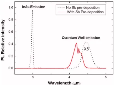
The observed improvement in the InAsSb MQW as a result of predeposition of Sb is in good agreement with pre-vious results obtained using MOVPE. Pillai et al. have stud-ied the effect of Sb predeposition on the compositional pro-file of InAs0.80Sb0.20/ InAs superlattices and observed Sb segregation for samples grown with no predeposition.7 For samples grown with 0.8 ML Sb predeposition, sharper In-AsSb on InAs interfaces were obtained. Sb coverages of⬎1 ML resulted in broader x-ray satellite peaks and rougher in-terfaces. Kaspi and Evans showed that an Sb floating layer forms on a III-V alloy surface.8By using the fact that Sb is more volatile than As and choosing a suitable As exposure time, the Sb floating layer can be removed. In our work a 20 s As exposure was used to remove this floating layer and thus prevent Sb incorporation into the InAs barrier layers. Our results indicate that these benefits carry over to the lu-minescence efficiency with the best EL being obtained from the samples with the sharpest interfaces. We also found that the luminescence emission intensity from the MQW is en-hanced compared with samples grown without any predepo-sition or As exposure. This enhancement becomes more sig-nificant as the Sb content in the MQW increases. A comparison of the emission spectra from samples prepared with and without the Sb predeposition is shown in Fig. 5. The MQW grown with predeposition exhibit emission at shorter wavelengths which we associate with reduced bow-ing in the valence band arisbow-ing from the more abrupt inter-faces with less structural disorder. We note that the bowing parameter in InAsSb is almost entirely determined by struc-tural disorder.9 Hence, changes in structural perfection will have a significant effect on the bowing parameter and con-sequently on the dependence of band gap on composition and the corresponding transition energy of the InAsSb in the MQW. Previously we reported the InAsSb conduction band bowing to be near 40% for samples grown without Sb predeposition.10The present results indicate that a value near 60% would be more appropriate for MQW grown using Sb predeposition.
In summary, mid-infrared electroluminescence from InAs0.87Sb0.13/ InAs MQW homojunction LEDs grown by MBE has been observed near 4.0m. The recombination was identified as originating from type II transitions
involv-ing confined holes and persisted up to room temperature with improved quenching behavior compared with the equivalent bulk alloy. The use of Sb predeposition during epitaxial growth produced MQWs with more abrupt interfaces which had a major effect on the electroluminescence. Both the best luminescence and the narrowest x-ray satellite peak width were obtained for an Sb predeposition time of 3 s. With some optimization of the structure and with the addition of an electron blocking barrier to confine the injected electrons, it should be possible to obtain significant further improve-ments in LED output and efficiency.
The authors wish to thank Kidde Ltd. for providing a CASE studentship for one of the authors共M.S.兲. The authors also wish to thank D. Campbell and G. Crook for valuable technical assistance and A. Godenir for x-ray measurements. 1A. Krier, H. H. Gao, V. V. Sherstnev, and Y. Yakovlev, J. Phys. D 32,
3117共1999兲.
2E. R. Glaser, B. R. Bennett, B. V. Shanabrook, and R. Magno, Appl. Phys.
Lett. 68, 3614共1996兲.
3G. Park, O. B. Shchekin, D. L. Huffaker, and D. G. Deppe, Appl. Phys.
Lett. 73, 3351共1998兲.
4A. Stein, D. Puttjer, A. Behres, and K. Heime, IEE Proc.: Optoelectron. 145, 257共1998兲.
5A. Krier, X. L. Huang, and A. Hammiche, Appl. Phys. Lett. 77, 3791
共2000兲.
6S. H. Wei and A. Zunger, Phys. Rev. B 52, 12039共1995兲.
7M. Pillai, S. C. Theiring, S. A. Barnett, B. W. Wessels, A. Desikan, and E.
P. Kvam, J. Cryst. Growth 208, 79共2000兲.
8R. Kaspi and K. R. Evans, J. Cryst. Growth 175/176, 838共1997兲. 9M. Ferhat, Phys. Status Solidi B 241, R38共2004兲.
10P. W. Liu, G. Tsai, H. H. Lin, and A. Krier, OPT Conference共Tainan,
Taiwan, 2005兲, paper. No. A-FR-II 4-2.
FIG. 5.共Color online兲 Comparison of the PL emission spectra from samples prepared with and without the Sb predeposition and As exposure.
091110-3 Krier et al. Appl. Phys. Lett. 89, 091110共2006兲