0040-6090/02/$ - see front matter䊚 2002 Elsevier Science B.V. All rights reserved. PII: S 0 0 4 0 - 6 0 9 0 Ž 0 2 . 0 0 1 3 7 - 2
Fabrication and characterization of aluminum oxide
ychromium oxide
superlattice for attenuated phase-shifting mask working at 193 nm
wavelength
F.D. Lai*, L.A. Wang
Department of Electrical Engineering and Institute of Electro-Optical Engineering, National Taiwan University, Taipei, Taiwan, ROC Received 21 July 2001; received in revised form 25 January 2002; accepted 12 February 2002
Abstract
A l O2 3yCr O superlattices with dense structures are successfully deposited on UV grade fused silica substrates and Si wafers2 3
by r.f. reactive unbalanced magnetron sputtering in a mixture of argon and oxygen gases at 150 8C. The dependence of the optical constant, plasma induced spectral intensity and deposition rate on the deposition parameters such as oxygen flow rate and r.f. sputtering power are examined. It was found that when O gas flow rate increases, the deposition rate and absorption of Al O2 2 3
and Cr O thin films decrease. The O2 3 yCr ratio of the CrO thin films identified by X-ray photoelectron spectroscopyx (XPS)
ranges from 1.5 to 3.0 when the sputtering power of the Cr target is increased from 20 to 80 W. The optical constants of Al O2 3y
Cr O superlattices and Al O and Cr O thin films are determined from the measured transmittance and reflectance by employing2 3 2 3 2 3
the reflection–transmittance(R–T) method. As for an attenuated phase-shifting mask (APSM) blank, it is found that when the
thickness percentages of Al O in Al O2 3 2 3yCr O superlattices are set between 60% and 70% the optical constants of superlattices2 3
can be tuned within the required R–T domain. Chemical and adhesion requirements of Al O2 3yCr O superlattices for APSM2 3
applications are also met.䊚 2002 Elsevier Science B.V. All rights reserved. Keywords: Optical properties; Aluminium oxide; Chromium oxide; Physical vapor deposition
1. Introduction
ArF based photolithography employing advanced res-olution enhancement technologies such as phase-shifting mask w1x, off-axis illumination w2x and optical proximity correction w3x can achieve patterns with dimension of less than 100 nm. Owing to destructive optical interfer-ence of light at the edges of circuit features, a phase-shifting mask improves depth of focus and resolution w4x. Since an attenuated phase-shifting mask (APSM) can overcome phase conflict problems for arbitrary mask patterns w5x and can be more easily fabricated than the other types of PSMs, it has attracted much attention in industry. Generally, the key requirements for an APSM blank are:(1) 1808 phase shift; (2) transmittance in the range of 4–15%; (3) reflectance less than 15%; (4)
*Corresponding author. Tel.: 2363-5251; fax: q886-2-2593-6897.
E-mail address: [email protected](F.D. Lai).
surface roughness less than 3 nm after the chemical durability test; and(5) good adhesion w6x.
Amulti-layer film having the property of very thin layers with a periodicity of less than 10% of a working wavelength is called a superlattice, and shall satisfy the effective medium theory w7x. Optical properties of such a superlattice are less sensitive to the details of layer interfaces w8x. As for materials, aluminum oxide w9x and chromium oxide w10x thin films exhibit very good properties such as chemical inertness, mechanical strength, hardness and optical characteristics; therefore, they have been widely used in many applications such as corrosion protection, wear resistance, electronics, and optics. However, they have not been reported for being used as APSM layers in the ArF lithography. In this work, we demonstrate that a new Al O2 3yCr O super-2 3
lattice whose dielectric constants are tunable can be used as an APSM blank layer for working at 193 nm wavelength.
Fig. 1. Plasma induced emission spectra of excited argon and oxygen atoms at the gas flow rates of:(a) O 10 sccm only, (b) Ar 10 sccm2
only,(c) Ar 10 sccm and O 4 sccm, (d) Ar 10 sccm and O 102 2
sccm, and(e) Ar 10 sccm and O 15 sccm.2
During the deposition process the plasma-induced emission spectra were monitored in situ in order to study the effect of each deposition parameter which might determine the final optical property and deposition rate of the aluminum oxide and chromium oxide thin films. As such, the Al O2 3yCr O superlattice prepared2 3
at the optimal deposition parameters are aimed to meet the optical, chemical and adhesion requirements of an APSM.
We report four main aspects in this paper:
1. the dependences of optical constant, plasma-induced spectral intensity and deposition rate on the deposition parameters such as oxygen flow rate and r.f. sputter-ing power of Al O and Cr O thin films are studied;2 3 2 3
2. the refractive index n and the extinction coefficient k
of Al O2 3yCr O superlattice deposited at the optimal2 3
conditions for Al O2 3 and Cr O2 3 thin films are characterized;
3. the thickness percentage ranges of Al O2 3 layer in A l O2 3yCr O superlattices that meet the optical requi-2 3
rements of APSM are experimentally obtained; and 4. the compositions of Al O2 3yCr O superlattices are2 3
characterized by the utilizing X-ray photoelectron
spectroscopy (XPS). We also use atomic force
microscopy (AFM) to study the surface roughness before and after chemical treatments and use Scotch tape to test adhesion.
2. Experiment
Al O , Cr O and Al O2 3 2 3 2 3yCr O superlattice thin films2 3
are deposited on UV grade fused silica substrates and also on polished Si wafers by using dual-gun r.f. reactive unbalanced magnetron sputtering in a mixture of argon and oxygen gases. Since a higher ion density can be obtained for an unbalanced magnetron sputtering system than a balanced one w11x, a more dense thin film can be obtained. The substrates are rotated during the dep-osition process to obtain uniform thin films. The sub-strates are cleaned in an ultrasonic bath by a series of processes: in trichlorethane for 5 min, distilled ion(DI) water for 10 min, acetone for 5 min, DI water for 10 min, ethanol for 5 min and DI water for 10 min. Target materials are chromium (99.99% purity) and aluminum (99.999% purity). Adeposition chamber surrounded by the heating girdles is evacuated to a base pressure of less than 1=10y6 torr using a cool trap and a diffusion pump. Prior to deposition the target is pre-sputtered for 20 min at 10 mtorr Ar pressure to remove AlO orx CrO contaminants from the target erosion track, andx for 1 h in the deposition parameters of the film deposited to poison the target surface and to fix the deposition rate and the property of the film. The substrate
temper-ature is controlled at 150"1 8C. The gas flow rate measured with the accuracy better than 0.1 sccm is controlled by the mass flow meter. The Ar flow rate is kept constant at 10 sccm in all deposition processes while the O flow rate is kept between 0 and 20 sccm.2
The O gas inlet rings with 0.5 mm holes per cm is2
placed around the Al and Cr targets and the O flow2
rate ratio for Al and Cr targets is set at ;1:4. The deposition parameters of the thin films are controlled by the gas pressure, gas flow rate and r.f. sputtering power. The plasma-induced emission of excited argon and oxygen atoms are characterized in situ by using a spectrometer, and the spectra are shown in Fig. 1. The significantly isolated wavelength peaks at 763.4 and 777.2 nm are from excited argon and oxygen atoms w12x, respectively. The refractive index n, extinction
coefficient k and deposition rates are analyzed and
correlated with the two emission wavelengths. The film thickness is measured by using an AFM, and reflectance and transmittance are measured by an ex situ optical spectrometer (Hitachi, U3501), which has high photo-metric accuracy (better than 0.01%). The refractive index and extinction coefficient of each film at 193 nm wavelength is obtained by the reflection–transmittance (R–T) method in which the multiple reflection effect is taken into account w13x. Each Al O2 3yCr O superlattice2 3
is composed of 10 Al O2 3yCr O film stacks with ;92 3
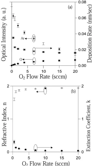
Fig. 2.(a) Variations of plasma induced emission intensities of excited
Ar and O atoms and deposition rate of Al O films with O flow2 3 2
rates. (b) Optical constants variation of Al O films with O flow2 3 2
rates.
layer’s thickness in the stack is controlled by deposition rate and time; therefore, the chemical compositions of A l O2 3yCr O2 3 superlattices can be determined. The chemical compositions of Al O and Cr O thin films2 3 2 3
are identified by utilizing XPS. An AFM is also used for the characterization of surface roughness before and after chemical durability measurement. The chemical durability of an Al O2 3yCr O superlattice is measured2 3
in the 90 8C solution (90% 10M H SO q10% H O )2 4 2 2
for 1 h and then in another 50 8C solution(1 M KOH) for 30 s. The adhesion between the Al O2 3yCr O super-2 3
lattice and the UV grade fused silica is analyzed by using Scotch tape.
3. Experiment results
The experiment errors of deposition rate, refractive index and extinction coefficient are less than 5%. How-ever, the experiment errors of optical intensity are less than 10%.
3.1. Deposition and optical property of Al O2 3 and Cr O thin films2 3
To understand the influence of plasma process on deposition rate and optical property of Al O2 3 and Cr O thin films, the plasma-induced emission spectra2 3
of excited argon and oxygen atoms are monitored during the deposition as mentioned previously.
3.1.1. Effects of O flow rate on Al O thin films2 2 3 The total chamber pressure and the Ar gas flow rate are, respectively, set at 8 mtorr and 10 sccm and the O gas flow rate varies from 0 to 20 sccm. Fig. 1 shows2
that as O flow rate increases the plasma-induced emis-2
sion intensity of excited Ar atoms becomes markedly lower and that of excited O atoms becomes higher. Fig. 2a shows that the deposition rate of Al O film depends2 3
on the plasma-induced emission intensity of excited Ar atoms, but not on the intensity of excited O atoms because the sputtering rate of the Ar plasma is higher than that of the O one. When the O flow rate increases,2
the partial pressure of Ar decreases and the oxide layer on the target surface is thicker. Therefore, it is seen that as the O flow rate increases, the Ar plasma intensity2
and the deposition rate become decreased. Since the probability of Al and O ions combination and the poison effect of O atoms on the Al target surface are higher at larger O2 partial pressure, the extinction coefficient becomes lower and the refractive index higher as shown in Fig. 2b. The variations of the extinction coefficients and the refractive indices are small as the O flow rate2
exceeds 10 sccm since Al is completely oxidized.
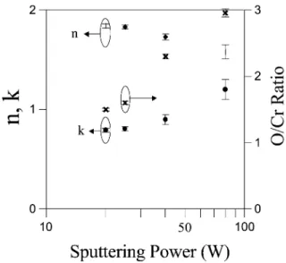
3.1.2. Effects of sputtering power on Al O thin films2 3 Fig. 3a depicts that plasma-induced emission intensi-ties of excited Ar and O atoms and the deposition rates of the films increase with sputtering power. The amounts of excited Ar and O atoms that bombard the Al target are increased significantly at high sputtering power; the deposition rate is therefore increased.
It is well known that the deposition of films depends on the diffusion rate when constituent particles strike a substrate w14x. When the diffusion rate is not high enough, voids are generated in the films. The diffusion rate of the particles is related to the sputtering power and the deposition pressure. Due to the diffusion rate being not high enough, the refractive index and extinc-tion coefficient of Al O2 3 films are lower at 50 W sputtering power than those at 85 W as shown in Fig. 3b. The structure of Al O film at 50 W is therefore not2 3
Fig. 3.(a) Variations of plasma induced emission intensities of excited
Ar and O atoms and deposition rate of Al O films with r.f. sputtering2 3
power.(b) Optical constant variation of Al O films with r.f. sputter-2 3
ing power.
Fig. 4.(a) Variations of plasma induced emission intensities of excited
Ar and O atoms and deposition rate of Al O films with total gas2 3
pressure.(b) Optical constant variation of Al O films with total proc-2 3
ess pressure.
dense. However, the high deposition rate at high sput-tering power causes impurities and loose structures in the films w15x. As shown in Fig. 3b, the extinction coefficient of Al O film is higher at 150 W sputtering2 3
power than that at 85 W due to some incompletely oxidized Al atoms left in the film.
3.1.3. Effects of gas pressure on Al O thin films2 3 The gas flow rates for both Ar and O are 10 sccm.2
When the gas pressure increases, the atom’s densities in the deposition chamber increase; therefore, the excited Ar and O atoms bombarding the target increase and their mean free paths decrease. Accordingly, plasma-induced emission intensities of excited Ar and O atoms and the deposition rate first increase and then decreases as shown in Fig. 4a. Fig. 4b depicts that the optical constants of Al O2 3 films are dependent on the total
deposition pressure and the extinction coefficient has a minimum at ;8 mtorr.
3.1.4. Plasma-induced emission intensity, deposition rate, and dielectric constant of Cr O thin films2 3
The characteristics of plasma induced emission inten-sities of excited Ar and O atoms, deposition rate, optical constants of a Cr O thin film are similar to those of an2 3
Al O thin film as mentioned previously except for the2 3
sputtering power. Fig. 5 depicts that the extinction coefficient at 193 nm wavelength at 20 W sputtering power is lower than at higher sputtering power.
3.2. Chemical composition analysis of Al O2 3 and Cr O thin films by XPS2 3
The ratio of OyAl in the Al O thin film identified2 3
by XPS is 1.5 in the following deposition parameters: 8 mtorr pressure, 85 W sputtering power, flow rates of 10
Fig. 5. Variations of optical constants and OyCr ratios in CrO thinx
films with r.f. sputtering power.
Fig. 6.(a) Calculated domain of desired optical constants and
meas-ured ones with various thickness percentage of Al O2 3 in the A l O2 3yCr O superlattice stacks. Indicated in parentheses are the2 3
thickness percentages of Al O2 3 in the Al O2 3yCr O2 3 superlattice stacks.(b) Variations of real (n yk ) and imaginary (2nk) parts of2 2
dielectric constants of Al O2 3yCr O superlattices with thickness per-2 3
centage of Al O .2 3
sccm for Ar and 20 sccm for O . The rates of O2 yA l in the AlO thin film in other deposition parameters arex slightly less than 1.5. At the same deposition parameters, the ratio of OyCr in the CrO thin film identified byx XPS ranges from 1.5 to 3.0 when the sputtering power in the Cr target is increased from 20 to 80 W as shown in Fig. 5. The chemical composition of CrO at higher3
sputtering power forms easier than at lower sputtering power. The CrO thin film deposited at 80 W sputtering3
power is unstable.
3.3. Optical property of Al O yCr O superlattices2 3 2 3 Superlattices are deposited at the same deposition parameters except that 85 W sputtering power is used for the Al target and 20 W for the Cr target.
The superlattice optical constants are calculated by modeling the multi-layer with a single homogeneous thin film. Fig. 6a depicts that the optical constants of A l O2 3yCr O2 3 superlattices are within the desired domain, i.e. transmittance between 4 and 15% and reflectance less than 15%, when the thickness percentage of Al O , which is defined as the ratio of Al O2 3 2 3
thickness in each stack thickness w16x, is set between 60 and 70%. Fig. 6b shows that the linear relationship of both real (n yk ) and imaginary (2nk) parts of the2 2
dielectric constant with the thickness percentage of Al O is verified and thus the dielectric constants of2 3
A l O2 3yCr O superlattices satisfy the effective medium2 3
theory. Al O2 3yCr O superlattices with tunable dielectric2 3
constants can then be easily used to design a desirable APSM blank. It has been reported that APSMs with 8– 10% high transmittance would minimize the side-lobe effect w17x. When the Al O2 3yCr O superlattice used as2 3
the APSM of 10% high transmittance and p-phase shift,
the calculated optimal thickness percentage of Al O ,2 3
reflectance and total thickness of the superlattices are 64.5%, 10.2% and 111.5 nm, respectively.
3.4. Surface roughness and transmittance variation of Al O yCr O superlattices before and after chemical2 3 2 3
durability test
3.4.1. Surface roughness
The surface roughness of the films before and after chemical durability test are measured by using an AFM. Fig. 7a shows the results for a surface within a 1=1 mm area before the chemical durability test, and Fig.2
Fig. 7. Surface roughness of Al O2 3yCr O superlattice2 3 (a) before and (b) after the chemical durability test.
surface roughness before the test is less than 0.5 nm and the maximum peak to peak magnitude is less than 1 nm. After the test, the mean value is less than 1 nm and the maximum less than 2 nm. Accordingly, the chemical corrosion rates of the Al O2 3yCr O superlatti-2 3
ces are small, and the calculated average phase shift decreases by less than ;28, which is within the accept-able range for APSM applications w6x. This is because both Al O and Cr O thin films exhibit good chemical2 3 2 3
inertness.
3.4.2. Transmittance variation
After the chemical durability test, the transmittance of Al O2 3yCr O superlattices increase less than 0.2%.2 3
This suggests that the film thickness decreases very little because Al O2 3yCr O superlattices have high resis-2 3
tance to chemical corrosion, which is in consistency with the result described in Section 3.4.1.
3.5. Adhesion test of Al O yCr O2 3 2 3 superlattices by Scotch tape testing
The adhesions among the films and to the fused silica substrate are very important. An investigation using Scotch tape in the ASTM Crosshatch tape testing method w6x is carried out on the films deposited on fused silica substrates. All the films pass the adhesion test. The adhesion strengths of the films are so strong that the films still adhere well with the substrates even though they are scratched by the Scotch Brite scouring pad. 4. Conclusion
A n A l O2 3yCr O2 3 superlattice with tunable optical constants is a new material candidate for APSMs to be working at 193 nm wavelength. Al O and Cr O thin2 3 2 3
films and Al O2 3yCr O superlattices with dense struc-2 3
tures are successfully deposited on UV grade fused silica substrates and Si wafers by r.f. reactive unbalance magnetron sputtering. It is found that deposition rates of the films are linearly proportional to the plasma-induced emission intensity of excited Ar atoms. The higher the O flow rates are, the lower the extinction2
coefficients, i.e. the oxidation of the films increases as evidenced by the plasma-induced emission intensity of excited O atoms. The ratios of OyAl in the AlO thinx films identified by XPS are equal to or slightly less than 1.5 while the ratios of OyCr in the CrO thin filmsx ranges from 1.5 to 3.0 when the sputtering power is increased from 20 to 80 W. The extinction coefficient of thin film at 193 nm wavelength at 20 W sputtering power is lower than at higher sputtering power. Al O2 3
and Cr O thin films deposited by employing the optimal2 3
deposition parameters are stoichiometric. Optical prop-erties of Al O2 3yCr O superlattices can be tuned by2 3
controlling the thickness percentage of Al O in Al O2 3 2 3y Cr O stacks. The optical constants are shown to be2 3
within the desired reflectance–transmittance domain when the thickness percentage of Al O2 3 in Al O2 3y Cr O2 3 superlattices is set between 60% and 70%. A l O2 3yCr O superlattices with tunable optical constant2 3
can be easily used as a desirable material blank for APSM. The dielectric constants of Al O2 3yCr O super-2 3
lattices are shown to fit the effective medium theory. And the calculated optimal thickness percentage of Al O in the Al O2 3 2 3yCr O superlattice used as APSM2 3
of 10% transmittance, with minimum side-lobe effect, and p-phase shift is 64.5%. Before and after the chem-ical durability test, the calculated average phase shift of the superlattices decreases by less than ;28, which is within the acceptable range for APSM applications. Strong adhesion strengths among Al O2 3yCr O super-2 3
lattice layers and to the UV grade fused silica substrates are obtained.
References
w1x M.D. Levenson, R.A. Simpson, IEEE Trans. Electron Devices
29(1982) 1828.
w2x M. Noguchi, M. Muraki, Y. Iwasaki, A. Suzuki, SPIE 1674 (1992) 741.
w3x A. Starikov, SPIE 1088(1989) 34.
w4x H. Watanabe, E. Sugiura, Y. Todokoro, M. Inoue, Jpn. J. Appl.
Phys. 30(1991) 3004.
w5x T. Terasawa, N. Hasegawa, H. Fukuda, S. Katagiri, Jpn. J.
Appl. Phys. 30(1991) 2991.
w6x P.F. Carcia, R.H. French, K. Sharp, J.S. Meth, B.W. Smith,
SPIE 2884(1996) 255.
w7x O. Hunderi, Physica A157(1989) 309.
w8x O. Hunderi, J. Wave-Mater. Interact. 2(1987) 29.
w9x E. Dorre, H. Hubner¨ (Eds.), Alumina: Processing Properties
and Applications, Springer, Berlin, 1984.
w10x P. Hones, M. Diserens, F. Levy, Surf. Coat. Technol. 120–121`
(1999) 277.
w11x W.D. Sproul, Surf. Coat. Technol. 49(1991) 284.
w12x R. Payling, D.G. Jones, A. Bengtson, Glow Discharge Optical
Emission Spectrometry, 1997.
w13x T.C. Paulick, Applied Optics 25(4) (1986) 562.
w14x J.A. Thornton, J. Vac. Sci. Technol. A. 4(6) (1986) 3059. w15x J.P. Bucher, K.P. Ackermann, F.W. Buschor, Thin Solid Films
122(1984) 63.
w16x P.F. Carcia, R.H. French, M.H. Reilly, M.F. Lemon, D.J. Jones,
Appl. Phys. Lett. 70(1997) 2371.
w17x Z. Cui, P.D. Prewett, S. Johnson, Microelectron. Eng. 27(1995)