Strain-induced growth of SiO
2dots by liquid phase deposition
C. W. Liua)Department of Electrical Engineering and Graduate Institute of Electronics Engineering, National Taiwan University, Taipei, Taiwan, Republic of China and Electronics Research and Service Organization, Industrial Technology Research Institute, HsinChu, Taiwan, Republic of China
B.-C. Hsu, K.-F. Chen, M. H. Lee, and C.-R. Shie
Department of Electrical Engineering and Graduate Institute of Electronics Engineering, National Taiwan University, Taipei, Taiwan, Republic of China
Pang-Shiu Chen
Electronics Research and Service Organization, Industrial Technology Research Institute, HsinChu, Taiwan, Republic of China
共Received 19 August 2002; accepted 9 December 2002兲
Silicon dioxide dots are deposited on the Si cap layers of self-assembled Ge dots using a liquid phase deposition method. The Si capping layer directly above the Ge dots has a tensile strain, while the Si cap on the wetting layer is not strained. The tensile strain can enhance the silicon dioxide nucleation and deposition on Si surface, and SiO2 dots are directly formed on the top of Ge dots with the SiO2 wetting layers between the dots. The step height and base width of the dots increase with the deposition time. A metal-oxide-semiconductor photodetector is fabricated using the liquid-phase-deposited oxide, and has a responsivity of 0.08 mA/W at 1550 nm. © 2003 American Institute of Physics. 关DOI: 10.1063/1.1542682兴
The SiGe/Si heterostructures have attracted great atten-tion in the high-speed electronics and optoelectronics applications.1,2 The strain engineering in the Si/Ge material system can change the band structures such as band discon-tinuity, effective mass, electron mobility, and the band de-generacy. Various heterojunction devices such as heterojunc-tion bipolar transistors 共HBT兲,3 high electron mobility transistors,4,5and strained Si/Ge channel field-effect transis-tors 共FET兲6,7were demonstrated. Strain can also control the layer growth, and self-assembled Ge dots on Si are demon-strated with material properties and optical properties.8,9 In this letter, we demonstrate the dot structures of silicon diox-ide can be grown on Si/Ge self-assembled layers with dot density similar to the underlying Ge dot density.
To avoid material degradation such as strain relaxation and Ge outdiffusion, the low-temperature oxide is often re-quired to reduce the thermal budget of SiGe device process. Liquid phase deposition 共LPD兲 is a promising low-temperature process for SiO2 formation with the advantages of low cost, selective growth, and high throughput. Based on the reaction of H2SiF6 with water to form hydrofluoric acid and solid SiO2,
10,11
the oxide prepared by liquid phase depo-sition can be deposited on Ge or Si substrates.12–15The Si/Ge quantum dots are used to generate local strain on Si layers, and are prepared by ultrahigh vacuum chemical vapor depo-sition 共UHVCVD兲 on p-type Si 共001兲 substrates. After a Si buffer layer of 50 nm was grown, 5 or 10 periods of Ge/Si bilayers were grown to form the self-assembled Ge dots at the temperature of 600 °C under the Stranski–Krastanov 共SK兲 growth mode.16,17
The Ge layers are separated by 20 nm Si spacer layers. A 3 nm共nominal thickness兲 Si cap was
deposited above the top layer of self-assembled Ge layer as the starting layer for the subsequent LPD oxide deposition. All ultrahigh vacuum chemical vapor deposition共UHVCVD兲 layers are p-type with the estimated concentration on the order of 1⫻1016cm⫺3. For comparison, rapid thermal oxi-dation共RTO兲 at 700 °C was also performed. During the LPD process, the silicic acid (SiO2:xH2O) was added to hydro-fluosilicic acid (H2SiF6,3 mol/L) at the temperature of 35 °C, and the solution was filtered to remove the undis-solved silica. H2O was then added to the saturated solution and enabled the solution to become supersaturated with sili-con oxide. Both quantum dots samples and the bare Si sili- con-trol samples were placed into the immersing solution at 50 °C together for different growth time. These samples were then taken out from the solution and rinsed with deionized water. The oxide thickness of control Si wafer was deter-mined by ellipsometry. The samples were characterized with atomic force microscopy 共AFM兲, and transmission electron microscopy共TEM兲 on 兵110其 cross sections of the samples.
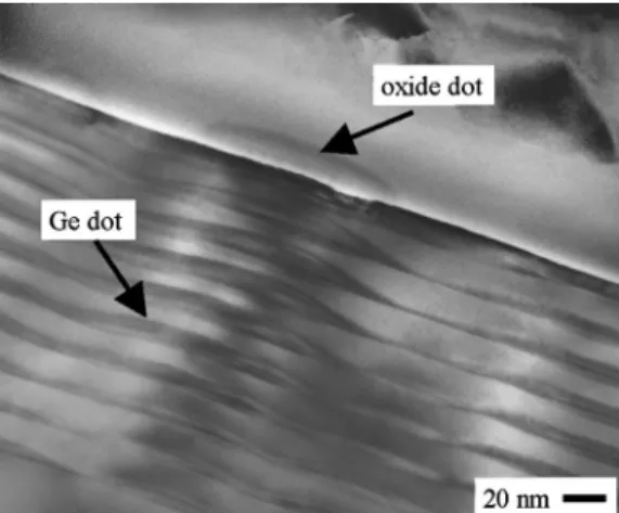
Figure 1 shows the cross-section TEM image of the ten-period Ge dots structure with the base and the height of ⬃100 and ⬃6 nm, respectively. The Ge layers are separated by⬃20 nm Si spacer layers. The Ge dots are self-assembled in a row vertically on the same position due to the spacer thickness smaller than the correlation length.8After 15 min LPD oxide growth, the SiO2 dots are formed on Si cap di-rectly above the Ge dots. Note that in the image, the central SiO2dot is clearly seen, while the dots on the left- and right-hand side exist, but the images are smeared. From the TEM images, the oxide dots have step height of 14 nm, and a wetting layer of 5 nm. The definition of the height is the step thickness between the oxide dot and the oxide wetting layer 关the inset of Fig. 2共a兲兴. The wetting layer is a thin layer of bright contrast above the Si cap in the TEM micrograph. The
a兲Author to whom correspondence should be addressed; electronic mail:
APPLIED PHYSICS LETTERS VOLUME 82, NUMBER 4 27 JANUARY 2003
589
thickness共5 nm兲 of wetting layer obtained from TEM micro-graph is similar to the oxide thickness共7 nm兲 on the control Si samples, measured by the ellipsometry using the refrac-tion index of 1.458. The step height 共14 nm兲 of oxide dots obtained from TEM is similar to AFM results 共15 nm兲. In Fig. 2共a兲, the oxide dot height obtained from AFM increases with the LPD deposition time up to 27 nm. The oxide thick-ness on control Si is also shown in Fig. 2共a兲, approximately indicating the thickness of the oxide wetting layer. The base of the oxide dots also increases with deposition time from 94 共10 min兲 to 176 nm 共25 min兲, as shown in Fig. 2共b兲. To confirm that the SiO2dots replicate at the sites of the Ge dots globally, AFM is performed on the five-period self-assembled Ge dots sample with a 20 nm Si spacer. The AFM image is shown in Fig. 3. The oxide dot density is 3 – 4 ⫻109 cm⫺2, very similar to the Ge dot density which is measured on the samples with the same growth condition without the top Si cap. This indicates that the deposited SiO2 dots are vertically aligned on embedded Ge dots. The mecha-nism of this alignment is probably related with the strain field on the Si cap. Due to the relaxation of Ge dots, the Si cap area directly on the Ge dots has tensile strain,8while the Si cap area above the Ge wetting layer is strain free共Fig. 4兲. The nucleation of oxide during LPD process may be much easier on the Si area with tensile strain than the strain-free Si area. Since the step height of oxide dots increases with depo-sition time faster than the oxide thickness on control Si as
shown in Fig. 2共a兲, the tensile strain also enhances the growth rates on tensile strained areas. The strain effect can last at least for oxide dot thickness of⬃45 nm 关sum of the oxide height and oxide thickness at the deposition time of 25 min in Fig. 2共a兲兴, since the step height still increases at this oxide thickness.
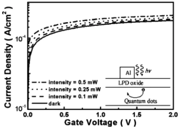
To have a metal–oxide–semiconductor共MOS兲 structure, aluminum is deposited on the LPD oxide and is patterned to form a MOS photodetector18 with a circular area of 3 ⫻10⫺4 cm2. The infrared of 1550 nm wavelength is shined on the edge of the MOS photodetector through an optical fiber. The photogenerated minority carriers共electron兲 can be collected by the gate electrode under the positive gate bias by diffusion and drift共as shown in the inset兲. A responsivity of 0.08 mA/W 共efficiency of ⬃1⫻10⫺4) is obtained with the dark current as 0.3 mA/cm2from the MOS photodetector. Figure 5 is the current–voltage curves with and without light exposure.
FIG. 1. Cross-section TEM micrograph of oxide dots on the self-assembled Ge quantum dots structures.
FIG. 2. 共a兲 Step height of LPD oxide dots and the oxide thickness on the control Si wafers vs LPD growth time. The oxide thickness on the control Si wafers is similar to the wetting layer thickness;共b兲 Base width of oxide dots as a function of deposition time.
FIG. 3. AFM surface image of LPD oxide on the Si cap layer of 5-period self-assembled Ge dot sample with 20 nm Si spacers.
FIG. 4. Schematic diagram of strain field distribution. The Si cap area above the Ge dots has a tensile strain, and the Si cap area on Ge wetting layers is strain free.
In summary, the strain field on the Si cap of self-assembled quantum dots can have preferential oxide deposi-tion during liquid phase deposideposi-tion process. The oxide dots are formed on the Si cap with tensile strain, and are aligned vertically with Ge dots embedded in the Si caps. The oxide wetting layer is deposited between oxide dots on the Si cap of self-assembled Ge dots. This strain controlled deposition is demonstrated in the LPD process, similar to the epitaxial quantum dot growth reported in Si/Ge system.
This work is partially supported by National Science Council, ROC, under Contract Nos. 共91-2120-E-002-007, and 91-2215-E-002-027兲.
1T. P. Pearsall, CRC Crit. Rev. Solid State Mater. Sci. 15, 551共1989兲. 2J. C. Bean, J. Vac. Sci. Technol. B 4, 1427共1986兲.
3C. A. King, J. L. Hoyt, and J. F. Gibbons, IEEE Trans. Electron Devices
36, 2093共1989兲.
4
K. Ismail, B. S. Meyerson, S. Rishton, J. Chu, S. Nelson, and J. Noccra, IEEE Electron Device Lett. 13, 229共1992兲.
5J. Welser, J. L. Hoyt, and J. F. Gibbons, IEEE Electron Device Lett. 15,
100共1994兲.
6
T. Mizuno, S. Takagi, N. Sugiyama, H. Satake, A. Kurobe, and A. Tori-umi, IEEE Electron Device Lett. 21, 230共2000兲.
7U. Konig and F. Schaffler, IEEE Electron Device Lett. 14, 205共1993兲. 8O. G. Schmidt and K. Eberl, Phys. Rev. B 61, 13721共2000兲.
9L. Vescan, T. Stoica, O. Chretien, M. Goryll, E. Mateeva, and A. Muck, J.
Appl. Phys. 87, 7275共2000兲.
10H. Nagayama, H. Honda, and H. Kawahara, J. Electrochem. Soc. 135,
2013共1988兲.
11T. Goda, H. Nagayama, A. Hishinuma, and H. Kawahara, Mater. Res. Soc.
Symp. Proc. 105, 283共1988兲.
12
B.-C. Hsu, W.-C. Hua, C.-R. Shie, K.-F. Chen, and C. W. Liu, Electro-chem. Solid State Lett.共to be published兲.
13A. Hishinuma, T. Goda, and M. Kitaoka, Appl. Surf. Sci. 49, 405共1991兲. 14C.-F. Yeh, C.-L. Chen, and G.-H. Lin, J. Electrochem. Soc. 141, 3177
共1994兲.
15J.-S. Chou and S.-C. Lee, Appl. Phys. Lett. 64, 1971共1994兲.
16T. I. Kamins, D. A. A. Ohlberg, R. S. Williams, W. Zhang, and S. Y. Chou,
Appl. Phys. Lett. 74, 1773共1999兲.
17
D. J. Eaglesham and M. Cerullo, Phys. Rev. Lett. 64, 1943共1990兲.
18
C. W. Liu, W. T. Liu, M. H. Lee, W. S. Kuo, and B. C. Hsu, IEEE Electron Device Lett. 21, 307共2000兲.
FIG. 5. Current–voltage curves of a MOS photodetector using the LPD oxide. The wavelength of infrared exposure is 1550 nm. The photogenerated carriers can be collected by lateral drift and diffusion.
591