國 立 交 通 大 學
電子物理研究所
博士論文
以鋁鎵銦砷半導體材料發展新的固態雷射技術
Investigation of novel solid-state laser technologies with
AlGaInAs semiconductor materials
學生:黃仕璋
指導教授:陳永富 教授
Investigation of novel solid-state laser technologies with
AlGaInAs semiconductor materials
研究生:黃仕璋 Student : Shih-Chang Huang
指導教授:陳永富 Advisor : Yu-Fung Chen
國立交通大學
電子物研究所
博士論文
A Thesis Submitted to Institute of Electrophysics
College of science
National Chiao Tung University
In Partial Fulfillment of the Requirements
For the Degree of Ph.D of Science
In Electrophysics June 2009
Hsinchu, Taiwan, Republic of China
以鋁鎵銦砷半導體材料發展新的固態雷射技術
學生:黃仕璋 指導老師:陳永富 教授
國立交通大學電子物理學系博士班
摘要
本論文是探討以 AlGaInAs 半導體材料發展新的固態雷射技術。以週期性結 構的量子井半導體材料作為增益介質以及半導體飽和吸收體。除了第一章的簡介 和末章的未來工作,主要內容分為三章:第二章主要集中在以光激發砷化鋁鎵銦 (AlGaInAs)半導體量子井材料,以主動式 Q 開關固態雷射作為光源,產生 1.06μm 雷射激發半導體雷射產生 1.36μm 和 1.57μm,應用在光通訊以及人眼安全。除此 之外,還以不同的激發機制(in-well pumping)達到功率優化的目的。第三章主要是 以砷化鋁鎵銦(AlGaInAs)半導體量子井材料作為被動式 1.06μm ,1.34μm Q 開關雷 射中的被動元件,也就是半導體飽和吸收體 以產生高峰值功率(kW)的雷射脈衝。第 四章主要是以砷化鋁鎵銦(AlGaInAs)半導體量子井材料作為被動式 1.34μm 鎖模 雷射中的被動元件,以產生短脈寬(~ps)的雷射脈衝。
Investigation of novel solid-state laser technologies
with AlGaInAs semiconductor materials
Student : Shin Cheng Huang Advisor: Prof. Yung-Fu Chen
Insitute and Department of Electrophysics
National Chiao Tung University
Abstract
The author demonstrates the investigation of novel solid-state laser technologies with AlGaInAs semiconductor materials. A periodic AlGaInAs quantum well / barrier based on Fe-doped InP substrate can be a semiconductor gain chip and a semiconductor saturable absorber. In addition to the introduction and the future work, the main text were divided into three chapter. In chapter two, AlGaInAs saturable absorber with a periodic QW/barrier structure that can be used to achieve an efficient high-peak-power and high average- power passively 1.06 and 1.34μm Q-switched lasers. In chapter three, AlGaInAs QWs grown on the Fe-doped InP substrate was designed to be a saturable absorber for self-starting continuous-mode-locked Nd:YVO4 laser at 1342 nm. In addition to be a saturable absorber, the periodic quantum well / barrier structure also can be a gain medium in solid-state laser. We demonstrated an AlGaInAs QW/barrier structure grown on an Fe-doped InP transparent substrate was developed to be a gain medium in a room-temperature high-peak-power nanosecond laser at 1.36 and 1.57μm for optical communication and eye-safe applications.
誌 謝
轉眼又到畢業的時候,時間過的真快,在交大的學習、生活已經過了五年了, 回想五年前,我只是個懵懵懂懂的研究生,經過了五年,修課、當助教、做實驗、 分析實驗、寫論文 …. 每一個過程都讓我有很大的收穫和成長。 在這裡,我要特別、非常感謝我的指導教授 – 陳永富老師。陳老師不僅在 學術上並且在做人處世、待人接物上,給了我很多指導。 在學術上,陳老師總是 保持非常高的熱忱以及高度的專注,尤其每當實驗說遇到問題時,老師總能適時 的分析並且耐心得給予指導和鼓勵。陳老師的這些指導和鼓勵就像天降甘霖一 般,給人在做實驗遇到挫折的時候還能夠繼續嘗試下去的勇氣。而在最後一段準 備口試的時間,陳老師給的震撼教育的確讓我有很大的進步,從研究動機、字型、 投影片的順序、參考文獻的排序…,老師給的建議都使我更注意這些細節的地方 而讓我的研究、論文可以更完整。另外,我也要非常感謝黃凱風老師,黃老師除 了提供我在實驗上的sample外,而且常常和我討論實驗數據以及未來的實驗方 向。而實驗室的同學︰蘇老大冠暐,亭樺,哲彥,偉立,興弛 ,依萍,雅婷,恩 毓,建誠,繼偉,漢龍(學長),彥廷,毅帆,威哲……感謝大家在實驗室生活各方 面的幫忙、照顧。 畢業或許是個結束,但是卻是人生另一階段的開始,感謝老師和同學幫我 在這個階段打下建立很好的基礎。Table of Content
摘要 ………..i
Abstract ……….ii
誌謝 ……….iii
Table of content ………iv
Figure of list ………..vi
Chapter One
.Introduction of solid-state laser technology
………..……...1Chapter Two
Semiconductor gain medium for pulsed laser
2.1 Introduction to Optically-Pumped Semiconductor laser (OPSL)………...52.2 Motivation and background………. 11
2.3. AlGaInAs quantum well 1.36μm laser………... 15
2.3.1 Device fabrication and laser structure……….15
2.3.2 Experimental result………..17
2.3.3 Conclusion………...20
2.4. AlGaInAs quantum well 1.57μm laser (barrier pumping)………...21
2.4.1 Laser structure and device fabrication……….21
2.4.2 Experimental results and discussion………23
2.3.3 Conclusion………...29
2.5. AlGaInAs quantum well 1.57μm laser (barrier pumping)………...30
2.5.1. Experiment setup………30
2.5.2. Experimental results and discussion………...31
2.5.3. Conclusion………..36
Chapter Three
Semiconductor saturable absorber (SESA) for Q-switched laser
3.1 Introduction of Q-switched laser ………...…38
3.2 Motivation and background……….…...39
3.3. Diode-pumped 1.06μm passively Q-switched laser ……….44
3.3.1 Device fabrication and experiment setup………...44
3.2.2 Experimental result and discussion……….46
3.3.3 Conclusion………...49
3.4. Diode-pumped 1.34μm passively Q-switched laser………..50
3.4.1 Device fabrication and experiment setup………..…………..50
3.4.2 Experimental result and discussion………...52
3.4.3 Conclusion………...56
3.5. Summary………....57
Chapter Four
Semiconductor saturable absorber (SESA) for mode-locked laser
4.1 Introduction ………...584.2 Motivation and background ………..61
4.3. Diode-pumped 1342-nm NdYVO4 passively mode-locked laser………...62
4.3.1 Device fabrication and experiment setup………..62
4.3.2 Experimental result and discussion ………..65
4.4. Summary and conclusion ………...67
Chapter Five Su
mmary and future work
……….68Reference
………70Figure of list
Fig.2.1.1: Schematic of an optically- pumped semiconductor disk laser ………...5 Fig.2.1.2 Band-gap diagram and operation principle of the OP-VECSEL……….6 Table 2.1.1.Summary of advantage and disadvantage of OPSL……….9 Table 2.1.2 The recent development of optically-pumped semiconductor laser………10 Fig.2.2.1 Schematic of barrier pumping (left) and in-well pumping (right)…………...13 Fig 2.3.1 The transmittance spectrum at room-temperature for AR-coated
AlGaInAs/InP gain chip ……….16 Fig. 2.3.2.Experiment configuration of 1.36μm optically pumped semiconductor
laser ………..17 Fig 2.3.3.Experimental results for the optically pumped AlGaInAs laser at pump
repetitionrates of 10, 40, and 100 kHz. ………..18 Fig. 2.3.4.(Color online) (a) Typical oscilloscope trace of a train of pump and output
pulses and (b) expanded shapes of a single pulse………. ….19 Fig. 2.3.5. Experimental results for the peak output power as a function of peak pump
power ………....20 Fig.2.4.1 Experimental configuration of the high-peak-power AlGaInAs QWs 1570-nm laser ………....21 Fig.2.4.2. Room-temperature spontaneous emission spectrum of the AlGaInAs QWs
pumped by a Q-switched Nd:GdVO4 1064-nm laser ………....23 Fig. 2.4.3 Experimental results for the optically pumped AlGaInAs 1570-nm laser
operated at the water temperature of 10°C ………..24 Figure 2.4.4 (a) Typical oscilloscope trace of a train of pump and output pulse and (b)
expanded shapes of a single pulse ………...25 Fig. 2.4.5 Experimental results for the peak output power as a function of peak pump
power at a repetition rate of 20 kHz ………..26 Fig. 2.4.6 Experimental results for the transmittance of the gain chip versus the
Fig. 2.4.7 Input–output characteristics for the water temperatures of 10, 15, 20, and 25°C at a repetition rate of 30 kHz ………28 Fig. 2.5.1. The schematic of the AlGaInAs/InP eye-safe laser at 1555 nm………30 Fig. 2.5.2. The performance of AlGaInAs 1555-nm laser in the scheme of barrier (line
with empty-square) and in-well pumping (line empty-circle), respectively……….32 Fig. 2.5.3 (a) Experimental results for the optically pumped AlGaInAs eye-safe laser
operated at 12°C for several pulse repetition rates……….33 Fig. 2.5.3 (b) Typical lasing spectrum at repetition rate of 40 kHz and average
pump ………....34 Fig. 2.5.4. The output characteristic was measured for the operation of different
temperature……….34 Fig. 2.5.5. The output peak power of AlGaInAs eye-safe laser at repetition rate of 20
kHz……….35 Figure. 3.2.1. Conduction band offset of AlGaInAs and InGaAsP semiconductor …..43 Fig. 3.3.1. An experimental diagram of a diode-pumped passively Q-switched
Nd:YVO4 laser using a periodic AlGaInAs QW/barrier structure as a saturable absorber ………..45 Fig. 3.3.2. Average output powers at 1064 nm with respect to the incident pump power
in cw and passively Q-switching operations………46 Fig. 3.3.3. Experimental results for the pulse repetition rate and the pulse energy versus
incident pump power………47 Fig. 3.3.4. Experimental results for the peak power and the pulse width (FWHM) as a
function of the incident pump power………....48 Fig. 3.3.5. (a) typical oscilloscope trace of a train of output pulses and (b) expanded
Fig3.4.1 The transmittance spectrum at room temperature for the AR-coated AlGaInAs saturable absorber……….51 Fig.3.4.2 An experimental setup of a diode-pumped 1.34μm passively Q-switched
Nd:YVO4 laser……….52 Fig.3.4.3 Average output power at 1342 nm with respect to the incident pump power in
cw and Q-switching operation………..53 Fig.3.4.4 Experimental result for the pulse energy with respect to the pump power
under pulse………54 Fig3.4.5 Experiment result for peak power with respect to pump power under pulse
pumping………....55 Fig.3.4.6 (a) Typical oscilloscope trace of a train of output pulses and (b) expanded
shape of a single pulse ……….56 Fig.4.3.1. Transmittance spectrum at room temperature for the AR-coated AlGaInAs
saturable absorber. Inset: schematic diagram of the AlGaInAs QW structure, where is the value of lasing wavelength………...63 Fig. 4.3.2. Schematic of a diode-pumped self-starting continuous-mode-locked
Nd:YVO4 laser at 1342nm. LD, laser diode ………64 Fig. 4.3.3 Average output power at 1342nm versus incident pump power in cw and
mode locked operations………....65 Fig. 4.3.4. (a) Typical oscilloscope trace of a train of mode-locked output pulses…....66 Fig. 4.3.5 Autocorrelation trace of the output pulses………..67
Introduction of solid-state technology
1.1 Diode pumped solid-state laser (DPSSL)
The solid state laser uses a solid crystalline material as the lasing medium and is usually optically pumped. Generally speaking, the gain medium of a solid state laser consist of a glass or crystalline host medium which is doped some rare-earth element such as neodymium-doped (Nd:YVO4 , Nd:YAG ), ytteribium-doped(Yb:YAG), and erbium doped (Er:YAG or Er-doped glass laser). In beginning of 1980s, the progress in the growth technology of semiconductor heterostructures allowed to develop the high-power diode laser. A solid gain medium pumped with a laser diode (LD) is so called diode-pumped solid-state (DPSS) lasers. The diode-pumped Nd:YAG lasers have operated at greater than 10 percent electric to optical efficiency in a single spatial mode. Furthermore, the high spectral power brightnessof these lasers has allowed frequency extension by harmonicgeneration in nonlinear crystals, which has led to green andblue sources of coherent radiation. Diode laser pumping hasalso been used with ions other than neodymium to produce wavelengthsfrom 946 to 2010 nanometers.
In addition, Q-switched operationwith kilowatt peak powers and mode-locked operation with picosecondpulse widths have been demonstrated in DPSS lasers. The progress in diode pumped solid-state laserspromises all solid-state lasers for high average powerlevels and at a price that is competitivewith flash-lamp pumped laser systems. Thus, the solid-state lasers have become the preferred candidates for a wide range of applications in science and technology including spectroscopy, atmospheric monitoring, micromachining, and precision metrology.
In solid-state laser physics, the lasing wavelength is determined by the doping and the host crystal properties. The limitation of discrete atomic levels is main drawback of crystalline gain medium. One area that demands particular attention is the wavelength spectrum near 1.3–1.6 µm, especially the “eye-safe” spectrum region (from 1.5µm-1.6µm). Extremely short and high-peak-power pulses of lasers at the eye-safe wavelength region are practically valuable for applications such as telemetry and range finders. The common gain medium to generate 1.3µm wavelength are Nd-doped crystals , and the methods for generating eye-safe lasers include the solid-state lasers with Er3+-doped or Cr4+-doped media and the stimulated Raman scattering (SRS) or optical parametric oscillators (OPO) pumped by Nd-doped lasers. In addition, the bandgap engineering and range of semiconductor materials systems provide potential spectral coverage from the near ultraviolet to the mid-infrared. This is a novel class of diode-pumped laser with a few micrometers pump absorption length. Hence, solid-state laser can be more compact by use of semiconductor materials.
The gain medium of semiconductor laser is direct-bandgap compound semiconductor materials. Different type semiconductor such as heterojunction, quantum well, edge emitting and surface emitting are widely applied in industry and scientific research. Besides, the optically pumped vertical-external cavity surface emitting laser (OP-VECSEL) overcomes the power limitation of vertical cavity surface emitting laser (VCSEL) and the beam quality of edge emitting laser(EEL). Thus, the OP-VECSEL technology has in fact become one of promising candidates to overcome the limitations of conventional semiconductor lasers. Moreover, the external cavity configuration allows other interesting application such as broadband laser absorption spectroscopy, single frequency operation, passive mode locking with a saturable absorber resulting in pico-second to femto-second pulse operation and
generating blue and green lights with intra-cavity frequency-doubling
Saturable absorber (SA) is the key element for pulse generation of solid-state laser. The passive saturable absorbers based on saturable optical absorption are of great interest due to their applications for Q switching and mode locking of near-infrared solid-state lasers to obtain short pulses of high peak power. The use of such laser pulses offers rich possibilities in material processing, optical telecommunication, range finding, industrial process control, atmospheric pollutions monitoring, medical diagnostics of diseases, laser surgery, and in scientific areas such as nonlinear optics and laser spectroscopy.
It is necessary for saturable absorber to possess low saturation intensity in conjunction with ultrafast relaxation time (or low saturation energy density together with slow absorption recovery time), high contrast of bleaching, high optical damage threshold, as well as good heat conduction and weak temperature dependence of the refractive index. Generally speaking, the ion-doped saturable absorbers (such as Cr4+:YAG) exhibit long recovery time and larger modulation depth for Q-switching operation. On the other hand, the absorption recovery times of semiconductor-based saturable absorbers are adequate both to Q-switched and to mode-locked lasers. The development of semiconductor saturable absorber mirror (SESAMs) is a novel family of optical devices that allow for very simple, self-starting, passive mode-locking of ultrafast solid-state and semiconductor lasers. This breakthrough device allowed the first demonstration of a passively mode-locked Nd:YLF laser - without Q-switching in 1992.
1.2 Guide to main text
The most important content in each chapter was sketchily pointed out here.
lasers. And we have demonstrated the periodic AlGaInAs QW/barrier structure grown on an Fe-doped InP transparent substrate was developed to be a gain medium in a room-temperature high-peak-power nanosecond laser at 1.36 µm and 1.57µm. In addition, for power scaling up, we also have demonstrated an optically pumped high-peak-power AlGaInAs/InP eye-safe laser by in-well pumping scheme. The conversion efficiency is enhanced over three times compared with barrier pumping scheme.
In chapter three, we demonstrate, for the first time to our knowledge, an AlGaInAs saturable absorber with a periodic QW/barrier structure that can be used to achieve an efficient high-peak-power and high average- power passively Q-switched lasers. The damage to the semiconductor saturable absorber can be ingeniously avoided by the periodic QW/barrier structure. Besides, compared with InGaAsP/InP QWs, AlGaInAs/InP QWs has larger conduction band offset which prevents carrier leakage at high temperature.
In chapter four, we have designed AlGaInAs QWs grown on the Fe-doped InP substrate to be a saturable absorber for self-starting continuous-mode-locked Nd:YVO4 laser at 1342 nm. Compare with other semiconductor saturable absorber (GaInNAs QWs and InAs/GaAs QD ), there is no need to anneal the AlGaInAs QWs to tune the PL wavelength and the optical characteristics of AlGaInAs QWs is more uniform than InAs/GaAs QDs. The present result confirms that the AlGaInAs QWs structures can be utilized to be saturable absorbers for the passively mode-locked lasers in the spectral region near 1.3 µm.
In chapter five, we give an overall conclusion of the entire work carried out in this thesis. Furthermore, we discuss the works and some interesting topics that we are going to do in the future.
Semiconductor gain medium for pulsed laser
2.1 Introduction to Optically-pumped semiconductor lasers (OPSL)
In 1997, M. Kuznetsov, F.Hakimi and A. Mooradian demonstrated for the first time a new high-power semiconductor laser technology, the optically-pumped semiconductor (OPS) vertical-external-cavity surface emitting laser (VECSEL) [1-2].
Optically-pumped semiconductor vertical-external surface emitting lasers (OP-VECSELs) has become one of promising candidates to overcome the limitations of conventional semiconductor laser. The OP-VECSELs combine the approaches of diode-pumped solid-states lasers and semiconductor quantum well vertical cavity surface emitting lasers (VCESL) and draw on the advantages of both. The OP-VECSELs can generate a multi-watt, near-diffraction-limited output beam with good efficiency in wavelength regions which are not covered by solid-state laser gain materials. Figure 2.1.1 shows the schematic of an optically pumped semiconductor disk laser [3-5].
Fig.2.1.1: Schematic of an optically- pumped semiconductor disk laser.
A VECSEL resembles the semiconductor quantum well active layers and a mirror structure contains a distribute Bragg reflectors (DBRs) and an external mirror. Semiconductor disc lasers are power-scalable because the active region is cooled by a one dimensional heat flow and the associated thermal gradient it’s along the axis of the optical cavity, minimizing the problems associated with thermal lensing and depolarization.
The layer structure of OP-VECSEL gain chip is shown in Fig2.1.2. In Fig2.1.2 a Bragg mirror, typically 25-30 periods, is grown next to the substrate [4-7]. The final layer in the design of the VECSEL is the capping layer. Its role is to prevent carrier diffusion from the quantum wells and also reduce oxidation of the VECSEL’s surface. The capping layer is made from semiconductor material which has a higher energy gap than that of the barrier region.
This acts as a barrier for those electrons with high energies, which can escape the well confinement. The additional benefit from this layer is that it can be grown to desired thicknesses. This can enhance the available gain from the laser by forming a
Substrate Multi-layer mirrors (DBRs)
Laser optical standing wave
Surface barrier
Cap layer
Pumping absorbing region λ/2 Quantum wells En er gy Semiconductor air
Substrate Multi-layer mirrors (DBRs)
Laser optical standing wave
Surface barrier
Cap layer
Pumping absorbing region λ/2 Quantum wells En er gy Semiconductor air
Substrate Multi-layer mirrors (DBRs)
Laser optical standing wave
Surface barrier
Cap layer
Pumping absorbing region λ/2 Quantum wells En er gy Semiconductor air
Substrate Multi-layer mirrors (DBRs)
Laser optical standing wave
Surface barrier
Cap layer
Pumping absorbing region λ/2 Quantum wells En er gy Semiconductor air
resonant structure in the small micro-cavity between the DBR and air surface. The most important feature of the RPG structure is that the position of the quantum-well active regions is arranged periodically such that they coincide with antinodes of a vertical standing wave pattern at the lasing wavelength. The spacer thickness determines the resonant wavelength at which the interaction of the optical field with the gain distribution is maximized. This structure has several advantages. First, since the gain medium only exists at the peaks of the standing-wave optical field, the spatial overlap integral between optical field and the gain elements is enhanced in the vertical direction (normal to the quantum well planes) at the resonant wavelength determined by the spatial periodicity of the gain medium. Hence, the gain in this structure is both anisotropic and wavelength selective. Second, charge carriers generated or injected tend to remain within the quantum wells and cannot at accumulate in the spacer regions, thus eliminating the possibility of longitudinal spatial hole burning. Moreover, loss of carriers through spontaneous emission is considerably reduced because the spacer medium around the nodes of the optical field contains no free carriers; this should result in a lower threshold and improved overall power efficiency.
Compared with optical pumping of semiconductor lasers, electrical pumping, in general, is the preferred approach. Electrically pumped VECSELs have a gain structure similar to that of a VCSEL, where a ring electrode around the active area injects carriers into that region. Current injection i.e. non-uniform current injection, current crowding, localize Joule heating, and free carrier absorption with attendant optical loss and excess heat deposition, are the major hurdles in the development of such large diameter devices. Non-uniform injection particularly favors higher-order transverse modes and reduces the transverse single mode wall-plug efficiency [8].
account of the controlled and uniform distribution of pump power over large active region and the absence of free carrier absorption, with attendant optical loss and excess heat deposition in the undoped active structure. Since optical pumping occurs via interband transition of the bulk barrier material, the pump absorption band is broad and imposes on practical constraint on the wavelength stability of the pump laser. The pumping absorption band is broad and absorption coefficient of the barrier material is typically ~ 0.8μm-1
such that pump radiation can be absorbed efficiently on a single or double pass of a very thin active region. Due to the very short absorption length of the semiconductor gain structure (at least for spacer pumping), the beam quality of the pump light is not very important. In general, for barrier pumping the carriers that are created by optical pumping in the barrier are trapped subsequently in the quantum wells. The gain bandwidth, differential gain, peak gain wavelength and quantum efficiency depend sensitively on carrier concentration and temperature. The active region is therefore affected by the pump power level, pumping spot-size, and thermal coupling to the heat sink more strongly than is the gain medium of a dielectric disc laser. An external laser cavity enforces output in a low divergence, circular, near diffraction-limited beam of high beam quality. With this external cavity configuration allows some interesting applications such as broadband laser absorption spectroscopy, single frequency operation, passive mode-locking with a saturable absorber resulting in pico-second to femto-second pulse operation and generating blue and green lights with intra-cavity frequency-doubling [9-17]. A summary of the main features, including advantages and disadvantages, of OPS- VECSELs is shown in Table 2.1.1 below.
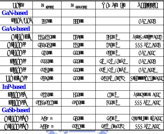
Table 2.1.2 shows the recent development of optically-pumped semiconductor laser [18-27]. Much work on the development of OP-VECSELs has used the high gain, compressively strained InGaAs/GaAs quantum well system. GaAs-based substrate optically pumped vertical external cavity semiconductor lasers (VECSEL) with high contrast GaAs/AlAs reflectors have operated in two wavelength regions: around 850nm using lattice-matched GaAs/AlGaAs quantum wells and around 1000nm using strained InGaAs/GaAs quantum wells [28-31]. For telecommunication application i.e. in the 1.3-1.55µm wavelength region, the natural material system is the InP-based. Unlike for GaAs-based semiconductor laser operating in 0.78-1.0µm short-wavelength range, the main obstacle for long-wavelength InP-based with low refractive index contrast semiconductor laser is the difficult realization of high-reflective Bragg mirrors (DBR) for 1.3-1.55µm long-wavelength region [32-36]. Moreover, this high thickness, combined with poor
(1)Intense localized heat is created in the semiconductor amounting to thermal roll over and limited powers. Thermal management techniques can be used to delay the arrival of roll-over losses.
(2)External cavity can make the overall size of the laser large in comparison to other semiconductor lasers.
Disadvantages
(1) Customized emission wavelength
(2) Bandgap engineering of the multi-QW semiconductors allows the design of laser medium with the desired laser properties.
(3) Broad pump bandwidth simplifies optical pumping with diodes (4) Very short pump absorption length leads to efficient pump absorption (5) No need for material doping or electric contacting
(6) Wide potential tuning range
(7) External cavity allows control of the output transverse mode and enables the incorporation of intra-cavity elements to control the laser spectral properties. Advantages
thermal conductivity of these materials and the high temperature sensitivity of the active layers lattice matched to InP, leads to poor thermal properties of semiconductor lasers.
GaN-based
GaAs-based
GaSb-based
InP-based
IEEE PTL 2004 0.6W at -18oC 1064nm 2.33μmAlGaAsSb
Cryst Growth 2004 8.5mW 830nm 2.3μmAlGaAsSb
IEEE PTL 2004 780mW 1250nm 1538-1545nmInGaAsP
Opt Comm 2004 45mW 980nm 1550nmInGaAsP
Electronic Lett 2004 0.612W at 5oC 810nm 1320nmGaInNAs
APL 2006 10W(CW) at RT 808nm 1060nmInGaAs
APL 2003 8W (CW) at RT 808nm 1000nmInGaAs
APL 2004 135mW 808nm 850nmAlGaAs
IEEE PTL 2003 523mW 660nm 830-860nmAlGaAs
Opt Express 2005 390mW 532nm 668-678nmAlGaInP
APL 2003 335nm 391nm InGaN/GaN Reference Max Power λpumping λlasing GainGaN-based
GaAs-based
GaSb-based
InP-based
IEEE PTL 2004 0.6W at -18oC 1064nm 2.33μmAlGaAsSb
Cryst Growth 2004 8.5mW 830nm 2.3μmAlGaAsSb
IEEE PTL 2004 780mW 1250nm 1538-1545nmInGaAsP
Opt Comm 2004 45mW 980nm 1550nmInGaAsP
Electronic Lett 2004 0.612W at 5oC 810nm 1320nmGaInNAs
APL 2006 10W(CW) at RT 808nm 1060nmInGaAs
APL 2003 8W (CW) at RT 808nm 1000nmInGaAs
APL 2004 135mW 808nm 850nmAlGaAs
IEEE PTL 2003 523mW 660nm 830-860nmAlGaAs
Opt Express 2005 390mW 532nm 668-678nmAlGaInP
APL 2003 335nm 391nm InGaN/GaN Reference Max Power λpumping λlasing Gain2.2 Motivation and background
2.2.1. AlGaInAs quantum well 1.36µm laser
High-peak-power all-solid-state laser sources in the 1.3–1.6 μm spectral region are of particular interest in remote sensing, eye-safe optical ranging, fiber sensing, and communication [1–4]. Diode-pumped solid-state lasers (DPSSLs) that have the advantages of relatively compact size, high power, excellent beam quality, long lifetime, and low heat production have been widely used for various applications, including industry, pure science, medical diagnostics, and entertainment [5]. Nevertheless, the spectral range of diode-pumped solid-state laser systems is limited by the properties of existing doped crystals and glasses. Recently, the optically pumped vertical-external-cavity surface-emitting semiconductor lasers (VECSELs) have been proposed as a novel class of all-solid-state lasers with potential spectral coverage from the near ultraviolet to the mid-infrared [6,7].
Typically, a VECSEL device consists of a highly reflecting distributed Bragg reflector (DBR) and a resonant periodic gain (RPG) structure that comprises a series of barriers to provide the pump absorption, quantum wells (QWs) to provide gain, and layers to prevent oxidation. Although InP-based material could offer a gain region with a smaller lattice mismatch for 1.3 μm wavelength, the small contrast of refractive indices hinders the performance of the DBRs. As a consequence, until now the InP-based material has never been used as a VECSEL device at 1.3 μm. To reach a wavelength near 1.3μm, GaInNAs/GaAs QWs have been developed as a gain medium[8] and a 0.6 W cw output power has been demonstrated [9]. Even so, there has been no experimental demonstration of room-temperature high-peak-power 1.3 μm laser sources with semiconductor QWs as gain media in an external cavity.
In this chapter, we report, for the first time to our knowledge, a room-temperature high-peak-power nanosecond semiconductor QW laser at 1.36 µm,
using a diode-pumped actively Q-switched Nd:GdVO4 1.06 µm laser as a pump source. With an average pump power of 1.85 W, an average output power of 340mW at a pulse repetition rate of 40 kHz was obtained corresponding to an optical-to-optical conversion efficiency of 18.4%. At a pulse repetition rate of 10 kHz, the peak output power was found to be up to 1.2 kW at a peak pump power of 7.9 kW
2.2.2. AlGaInAs quantum well 1.57µm laser
High-peak-power nanosecond pulsed lasers operating with emission at the eye-safe wavelength region (1.5–1.6 µm) are of great interest because of their potential applications, such as laser radar, active imaging, and remote sensing [10–12]. The methods for generating eye-safe lasers include the solid-state lasers with Er3+-doped or Cr4+-doped media [13–16] and the stimulated Raman scattering (SRS) [17–20] or optical parametric oscillators (OPO) [21–23] pumped by Nd-doped lasers. The advent of diode-pumped solid-state lasers (DPSSLs) [24–27] with high peak powers and excellent brightness leads to a renaissance of interest in wavelength conversions with the SRS or OPO process
Another practical approach for eye-safe laser sources is based on semiconductor quantum-well (QW) materials including InGaAsP and AlGaInAs systems [28–31]. Recently, a high-peak-power AlGaInAs laser at 1.36 µm was designed with a diode-pumped actively Q-switched Nd:YAG laser as a pump source [32]. Nevertheless, there has been no experimental demonstration of high-peak-power optically pumped AlGaInAs eye-safe laser.
In this chapter, a high-peak-power nanosecond AlGaInAs eye-safe 1.57-µm laser driven by a diode-pumped actively Q-switched Nd:GdVO4 laser is presented for the first time to our knowledge. An average output power of 135 mW with a pulse
width of 30 ns at a pulse repetition rate of 30 kHz was obtained with an average power of 1.5 W to pump an AlGaInAs QW/barrier structure grown on a Fe-doped InP transparent substrate. The maximum peak power was up to 290 W at a pulse repetition rate of 20 kHz.
On the other hand, the quantum defect, the energy difference between a pump and a laser photon, is the main source of heat generation in active region, the in-well pumping scheme has potential for high optical efficiency because of smaller quantum defect [33-39]. The quantum defect and the thermal load can be reduced by pumping the quantum well directly. Fig 2.2.1 shows a schematic diagram of barrier pumping and in-well pumping. Optical transition in barrier pumping: electron-hole pairs are generated in the barrier region and recombine via photon emission from the quantum well ground state levels in the conduction band. On the
QW Barrier Barrier En erg y ( eV) Position (nm) CB CB VB VB 1. 34 μ m 1. 06 4μ m 1.57μm 1.57μm Barrier QW Barrier QW Barrier Barrier En erg y ( eV) Position (nm) CB CB VB VB 1. 34 μ m 1. 06 4μ m 1.57μm 1.57μm Barrier QW Barrier
contrary, optical transitions for quantum well pumping: electron-hole pairs are generated inside the quantum well with energies slightly above the ground state energy. In contrast to barrier-pumping scheme, the quantum defect is considerably reduced by in-well pumping.
However, a problem arising for in-well pumping is the short absorption length, since the quantum wells are only a few nanometers thick. Higher numbers of quantum wells lead to longer total absorption lengths, but also result in a higher laser threshold. To increase the pump efficiency, a resonant absorption scheme was introduced. Another approach to increase the absorption length is a multi-pass pump setup, which is a well-known concept for dielectric solid state thin disk lasers [40-50]. Multi-pass pumping can also be combined with resonant absorption for further improvement of the absorption efficiency. A decreased thermal shift of the output wavelength for in-well pumping indicates a significantly reduced thermal load compared to
barrier pumping. Several reports of an in-well pumping laser have been
demonstrated with wavelength in the range of 800 nm to 2.35µm except to 1.55µm. In this chapter, we have demonstrated an efficient high-peak-power AlGaInAs eye-safe laser at 1570 nm. The quantum defect and the thermal load are significantly reduced by pumping the quantum well directly. The overall conversion efficiency is enhanced over three times compared with the barrier pumping method. With a pump peak power of 3.7 kW, an output peak power of 0.52 kW is generated at a pulse repetition rate of 20kHz.
2.3. AlGaInAs quantum well 1.36µm laser
2.3.1 Device fabrication and laser structure
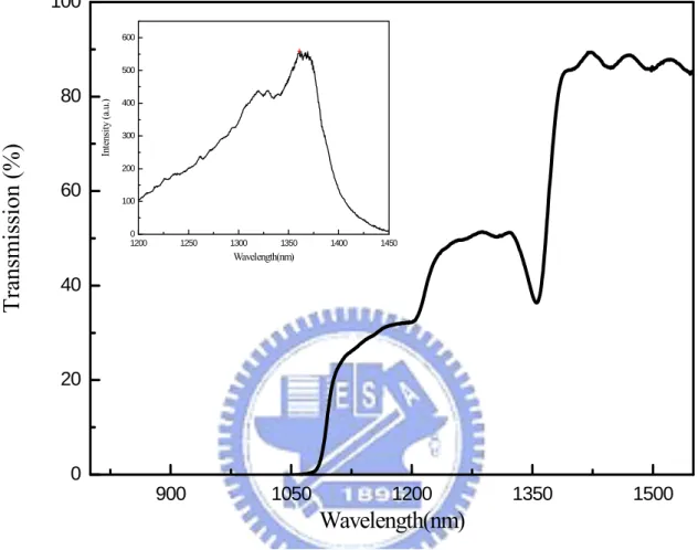
The present gain medium is an AlGaInAs QW/barrier structure grown on an Fe-doped InP substrate by metal-organic chemical-vapor deposition (MOCVD). It is worthwhile to mention that the AlGaInAs material system has a larger conduction band offset than the most widely used InGaAsP system [1–4]. This larger conduction band offset has been confirmed to yield better electron confinement in the conduction band and higher temperature stability. The AlGaInAs material has been used as a surface-emitting optical amplifier pumped by a laser diode [5]. However, until now there has been no experimental realization involving the VECSEL with AlGaInAs. Here the gain region consists of 30 groups of two QWs with the luminescence wavelength around 1365 nm, spaced at half-wavelength intervals by AlGaInAs barrier layers with the bandgap wavelength around 1070 nm. The barrier layers are used not only to absorb the pump light but also to locate the QW groups in the antinodes of the optical field standing wave. An InP window layer was deposited on the gain structure to avoid surface recombination and oxidation. The back side of the substrate was mechanically polished after growth. Both sides of the gain chip were antireflection (AR) coated to reduce back-reflections and coupled-cavity effects. The total residual reflectivity of the AR-coated sample is approximately 5%. Figure 4.3.1 shows the transmittance spectrum at room temperature for the AR-coated AlGaInAs/InP gain chip. It can be seen that the strong absorption of the barrier layers leads to low transmittance near 1070 nm. The total absorption efficiency of the barrier layers at 1064 nm was found to be approximately 95%. On the other hand, an abrupt change in transmittance near 1365 nm comes from the absorption of the AlGaInAs QWs. The room-temperature spontaneous-emission spectrum, obtained by pulse excitation at 1064 nm, is shown in
the inset of Fig2.3.1. As expected, the emission is quite broad, with a peak around 1365 nm, and has a long tail extending to shorter wavelengths.
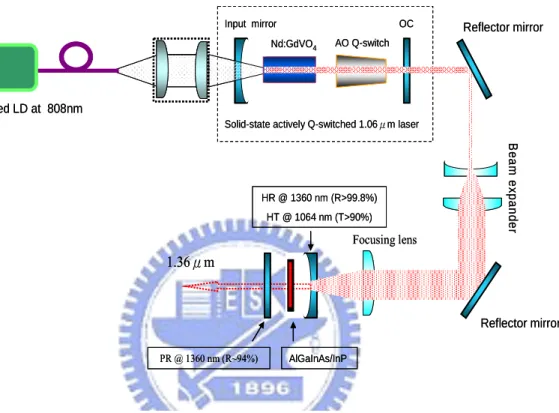
Figure 2.3.2 shows the experimental configuration of the room-temperature high-peak-power AlGaInAs QWs laser at 1365 nm. The pump source is a diode-pumped acousto-optically Q-switched Nd:GdVO4 1064 nm laser to provide 12-90 ns pulses at repetition rates between 10 and 100 kHz. The pump spot diameter is controlled to be 380±20 μm for efficient spatial overlap with the fundamental transverse mode. The gain chip was mounted on a copper heat sink, but no active cooling was applied. The laser resonator is a concave–plano cavity. The input mirror was a 500 mm radius-of-curvature concave mirror with AR coating on the
900 1050 1200 1350 1500 0 20 40 60 80 100 1200 1250 1300 1350 1400 1450 0 100 200 300 400 500 600 In te ns ity (a .u .) Wavelength(nm)
Tran
smissi
on
(%)
Wavelength(nm)
Fig 2.3.1: The transmittance spectrum at room-temperature for AR-coated AlGaInAs/InP gain chip Inset : Room-temperature spontaneous-emission spectrum by 0.8W pulse excitation at 1064nm.
entrance face at 1064 nm (R<0.2%), high-reflection coating at 1365 nm (R>99.8%), and high-transmission coating at 1064 nm on the other surface (T>90%). The reflectivity of the flat output coupler is 94% at 1365 nm. The overall laser cavity length is approximately 10 mm.
2.3.2 Experimental result
Figure 2.3.3 shows the performance of the optically pumped AlGaInAs laser at pump repetition rates of 10, 40, and 100 kHz. The pump pulse widths for repetition rates of 10, 40, and 100 kHz are approximately 12, 35, and 75 ns, respectively. The cavity decay time is approximately 0.11 ns. The beam quality factor was determined by a Gaussian fit to the laser beam waist, and the divergence angle and was found to be less than 1.5. At a repetition of 40 kHz, the average output power could be up to 340 mW; the output power saturation beyond the average pump power of 1.8 W was due to the thermally induced gain degradation. At a repetition of 10 kHz, the absorption efficiency of the gain chip for the pump power higher than 0.8 W was found to be
Nd:GdVO4 Input mirror Fiber coupled LD at 808nm OC AO Q-switch HR @ 1360 nm (R>99.8%) HT @ 1064 nm (T>90%) PR @ 1360 nm (R~94%) AlGaInAs/InP Reflector mirror Reflector mirror Focusing lens B e am e x pan d e r
Solid-state actively Q-switched 1.06μm laser
1.36μm Nd:GdVO4 Input mirror Fiber coupled LD at 808nm OC AO Q-switch HR @ 1360 nm (R>99.8%) HT @ 1064 nm (T>90%) PR @ 1360 nm (R~94%) AlGaInAs/InP Reflector mirror Reflector mirror Focusing lens B e am e x pan d e r
Solid-state actively Q-switched 1.06μm laser
1.36μm
significantly reduced because of pump-saturation effects of the barrier layers. As a consequence, maximum average output power at a repetition rate of 10 kHz was saturated at around 120 mW. With the experimental data on a pump pulse energy of 80 μJ, a pump pulse width of 15 ns, and a pump area of 0.113 mm2, the pump saturation intensity was estimated to be 4.7 MW/cm2. This value was 2–3 orders of magnitude higher than conventional solid-state laser crystals because of its shorter fluorescence decay time [6]. However, the lower conversion efficiency at the 100 kHz repetition rate might be due to the longer pump pulse duration that enhanced the local heating effect. The maximum output power at 100 kHz was found to be nearly the same as the result obtained at 10 kHz. In other words, management of the thermal effects is necessary to scale up the average output power.
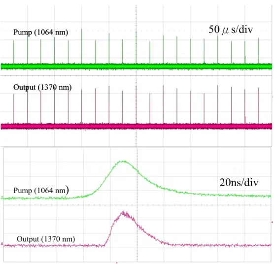
Figure 2.3.4 shows a typical oscilloscope trace of a train of output and pump
0.0 0.4 0.8 1.2 1.6 2.0 2.4 0 60 120 180 240 300 360
Ave
rage out
put
power at
1370nm (mW)
Incident pump power at 1064nm (W)
10kHz
40kHz
100kHz
Fig 2.3.3 Experimental results for the optically pumped AlGaInAs laser at pump repetition rates of 10, 40, and 100 kHz.
pulses and expanded shapes of a single pulse. It can be seen that the output pulses tracked the pump pulses for each pumping case. Figure 2.3.5 shows the peak output power as a function of peak pump power. The peak output power was up to 1.2 kW at a peak pump power of 7.9 kW, and the slope efficiency was approximately 15.2%. The typical lasing spectrum shown in the inset of Fig. 2.3.5 was obtained with 1.2W of average pump power at a repetition rate of 40 kHz. The lasing spectrum was composed of dense longitudinal modes, and its bandwidth was up to 20 nm for an average pump power greater than 500 mW. The wide spectral range indicates the potential for achieving ultra-short pulses in mode-locked operation.
50μs/div
20ns/div
Pump (1064 nm) Pump (1064 nm)
Output (1370 nm) Output (1370 nm)50μs/div
50μs/div
20ns/div
Pump (1064 nm) Pump (1064 nm)
Output (1370 nm) Output (1370 nm)20ns/div
Pump (1064 nm) Pump (1064 nm)
Output (1370 nm) Output (1370 nm)Fig. 2.3.4 (Color online) (a) Typical oscilloscope trace of a train of pump and output pulses and (b) expanded shapes of a single pulse.
2.3.3 Conclusion
In summary, an AlGaInAs QW/barrier structure grown on an Fe-doped InP transparent substrate was developed to be a gain medium in a room-temperature high-peak-power nanosecond laser at 1365 nm. Using an actively Q-switched 1064 nm laser to pump the gain chip, an average output power of 340 mW was obtained at a pulse repetition rate of 40 kHz and an average pump power of 1.9 W. At a pulse repetition rate of 10kHz, the peak output power was found to be up to 1.2 kW at a peak pump power of 7.9 kW
1360 1365 1370 1375 1380 1385 1390 0 2000 4000 6000 8000 10000 12000 14000 In te ns ity( arb . u nit) Wavelength(nm) 0 1 2 3 4 5 6 7 8 0.0 0.2 0.4 0.6 0.8 1.0 1.2 Pe ak out put powe r a t 1365nm (kW)
Peak incident pump power at 1064nm (kW)
1360 1365 1370 1375 1380 1385 1390 0 2000 4000 6000 8000 10000 12000 14000 In te ns ity( arb . u nit) Wavelength(nm) 0 1 2 3 4 5 6 7 8 0.0 0.2 0.4 0.6 0.8 1.0 1.2 Pe ak out put powe r a t 1365nm (kW)
Peak incident pump power at 1064nm (kW)
Fig. 2.3.5. Experimental results for the peak output power as a function of peak pump power. Inset, typical lasing spectrum obtained with 1.2W of average pump power at a repetition rate of 40 kHz
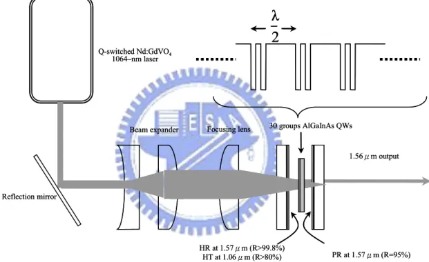
2.4. AlGaInAs quantum well 1.57µm laser (barrier pumping)
2.4.1 Laser structure and device fabrication
Figure 2.4.1 shows the experimental configuration of the high peak-power AlGaInAs QWs 1570-nm laser pumped by a diode actively Q-switched Nd:GdVO4 laser. The pump source provides 20–60 ns pulses at repetition rates between 20 and 60 kHz. The pump spot diameter was controlled to be 480±20 µm for efficient spatial overlap with the fundamental transverse mode.
The laser resonator is a linear flat–flat cavity that was stabilized by the thermally induced lens in the gain medium. This concept was found nearly simultaneously by Zayhowski and Mooradian [1] and by Dixon et al. [2]. A linear flat–flat cavity is an attractive design because it reduces complexity and makes the system compact and rugged. When the average pump power is between 0.5 and 1.5 W, the mode-to-pump ratio is experimentally found to be in the range of 1.0–1.5. The input mirror was a flat mirror with antireflection coating on the entrance face at 1064 nm (R
Beam expander Focusing lens
Reflection mirror Q-switched Nd:GdVO4 1064–nm laser
λ
2
1.56μm output 30 groups AlGaInAs QWs HR at 1.57μm (R>99.8%) HT at 1.06μm (R>80%) PR at 1.57μm (R=95%) Beam expander Focusing lensReflection mirror Q-switched Nd:GdVO4 1064–nm laser
λ
2
λ
2
1.56μm output 30 groups AlGaInAs QWs HR at 1.57μm (R>99.8%) HT at 1.06μm (R>80%) PR at 1.57μm (R=95%)Fig. 2.4.1 Experimental configuration of the high-peak-power AlGaInAs QWs 1570-nm laser pumped by a Q-switched Nd:GdVO4 laser; HR: high reflection, HT: high transmission,
<0.2%), high-reflection coating at 1570 nm (R > 99.8%), and high-transmission
coating at 1064 nm on the other surface (T >90%). The reflectivity of the flat output coupler is 95% at 1570 nm. The overall laser cavity length is approximately 10 mm.
The present gain medium is an AlGaInAs QW/barrier structure grown on a Fe-doped InP substrate by metal-organic chemical-vapor deposition (MOCVD). Note that the conventional S-doped InP substrate has large absorption in the 1.0–2.0 µm spectral region, while the Fe-doped InP substrate is chosen because of its transparency at the lasing wavelength. The gain region is made up of thirty groups of two 8-nm-thick 1570-nm AlGaInAs QWs with 10-nm-thick barriers. Each QW group is spaced at a half-wavelength interval by an AlGaInAs barrier layer with the band-gap wavelength approximately 1064 nm to absorb the pump light as well as to locate the QWs in the antinodes of the optical standing wave. An InP window layer was deposited on the gain structure to avoid surface recombination and oxidation. The backside of the substrate was mechanically polished after growth. The both sides of the gain chip were antireflection-coated (AR-coated) to reduce back reflections and the couple-cavity effects. For simplicity, we used a single layer of coating on the gain medium. As a result, the total residual reflectivity of the AR-coated sample is approximately 5%.
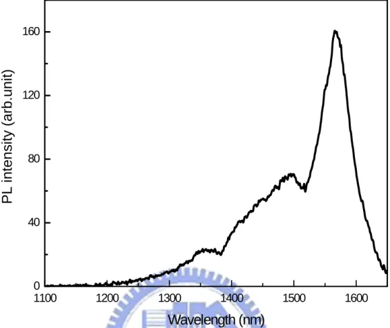
Figure 2.4.2 depicts the room-temperature spontaneous emission spectrum obtained by pulse excitation at 1064 nm. It can be seen that the emission is quite broad with a peak at around 1570 nm and has a long tail extending to shorter wavelength. In the laser experiment, the semiconductor chip was simply mounted on a water-cooled copper block and the water temperature was feedback maintained.
2.4.2 Experimental results and discussion
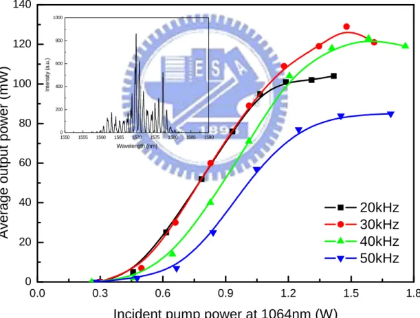
Figure 2.4.3shows the performance of the optically pumped AlGaInAs laser operated at the water temperature of 10°C at four repetition rates of 20, 30, 40, and 60 kHz. The pump pulse widths for the repetition rates of 20, 30, 40, and 60 kHz are approximately 20, 25, 30, and 40 ns, respectively. The transverse mode was measured to be the fundamental mode over the complete output power range. The beam quality factor was determined by a Gaussian fit to the laser beam waist and the divergence angle, and was found to be less than 1.3 indicating fundamental transverse-mode operation. Spectral information of the laser was monitored by an optical spectrum analyzer (Advantest Q8381A). The spectrum analyzer with a diffraction monochromator can be used for high-speed measurement of pulse light with a resolution of 0.1 nm. It was found that the bandwidth of the lasing spectrum initially
1100 1200 1300 1400 1500 1600 0 40 80 120 160
PL i
n
ten
s
it
y (
a
rb.un
it)
Wavelength (nm)
Fig.2.4.2. Room-temperature spontaneous emission spectrum of the AlGaInAs QWs pumped by a Q-switched Nd:GdVO4 1064-nm laser
increases linearly with the pump power but varies slowly at the higher pump power. The lasing spectrum has the highest peak approximately at 1570 nm with maximum bandwidth up to 18 nm. The typical lasing spectrum shown in the inset of Fig. 2.4.3 was obtained with 1.0 W of average pump power at repetition rate of 30 kHz. The lasing spectra generally comprised dense longitudinal modes and their bandwidth were up to 20 nm at the average pump power greater than 200 mW. The temporal shapes for pump and output pulses were recorded by a LeCroy digital oscilloscope (Wave pro 7100, 10 G samples/s, 1 GHz bandwidth).
0.0 0.3 0.6 0.9 1.2 1.5 1.8 0 20 40 60 80 100 120 140 1550 1555 1560 1565 1570 1575 1580 1585 1590 0 200 400 600 800 1000 In te n s ity (a .u .) Wavelength (nm)
Av
erage output power (mW
)
Incident pump power at 1064nm (W)
20kHz
30kHz
40kHz
50kHz
Fig. 2.4.3 Experimental results for the optically pumped AlGaInAs 1570-nm laser operated at the water temperature of 10°C at pump repetition rates of 20, 30, 40, and 60 kHz. Inset shows typical lasing spectrum obtained with 1.0 W of average pump power at a repetition rate of 30 kHz
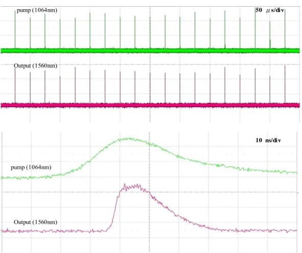
Typical oscilloscope traces of pump and output pulses are shown in Fig. 2.4.4.With the finest alignment, the pulse-to-pulse amplitude fluctuation was found to be within ±10%, which is mainly attributed to the instability of the pump beam. As shown in Fig. 2.4.3, the average output power at a repetition rate of 30 kHz initially increases with the pump power and begins to saturate at 135 mW at an average pump power greater than 1.25W. Similarly, the conversion efficiency at a repetition rate of 20 kHz is reduced significantly at the average pump power greater than 1.0W and the maximum average output power is saturated at approximately 115mW. The reduction of the conversion efficiency at higher pump powers mainly comes from the gain-saturation effect. pump (1064nm) pump (1064nm) Output (1560nm) Output (1560nm) 10 ns/div 50 μs/div
Figure 2.4.4 (a) Typical oscilloscope trace of a train of pump and output pulse and (b) expanded shapes of a single pulse
Figure 2.4.5shows the output peak power as a function of pump peak power at a repetition rate of 20 kHz. The maximum output peak power is found to be 290 W at a pump peak power of 2.3 kW. With the transmission of the output coupler of 5%, the maximum intra-cavity lasing power can be calculated to be 5.8 kW. We use the formula A = π(ωL)2 to calculate the lasing mode area, where ωL is the lasing mode size. Using ωL = 250 µm, the lasing mode area and the saturation intensity of the gain chip can be found to be 0.002 cm2 and 2.9 MW/cm2, respectively. This value was two orders of magnitude higher compared to conventional solid-state laser crystals because of its shorter fluorescence decay time. To confirm the gain-saturation effect we used a pulsed semiconductor laser at 1.57 µm to measure the transmittance versus the excitation intensity with the z-scan method. The excitation pulse energy and pulse width were 3 µJ and 50 ns, respectively. The pump radius was varied from 0.01 to 0.1 cm. As a consequence, the excitation fluence was in the range of 0.1–10 mJ/cm2 and was comparable to the fluence in the present laser cavity.
0.0 0.5 1.0 1.5 2.0 2.5 3.0 0 80 160 240 320 Ou tp ut pe ak powe r (W)
Pump peak power (kW)
Fig. 2.4.5 Experimental results for the peak output power as a function of peak pump power at a repetition rate of 20 kHz
As shown in Fig. 2.4.6, the transmittance of the gain material exceeds 85% at the excitation intensity higher than 3.0 MW/cm2. Therefore, the number of QWs in the gain chip needs to increase to overcome the gain-saturation effect for scaling up the output peak power. On the other hand, the lower conversion efficiency at 60 kHz is speculated to arise from the longer pump pulse width at this repetition rate leading to the heavier heating effect. We examined the dependence of lasing efficiencies on the water temperature to investigate the influence of the thermal effect.
Figure 2.4.7depicts the input–output characteristics for the water temperatures of 10, 15, 20, and 25°C at a repetition rate of 30 kHz. Increasing temperature can be seen to lead to a certain reduction in the lasing efficiency. Compared with the experimental results shown in Fig. 2.4.3 it can be found that the maximum output power at 20°C at a repetition rate of 30 kHz is almost comparable with that at 10°C at
0.01 0.1 1 10 40 60 80 100 T ran sm ittan ce ( %)
Excitation energy density (mJ/cm2)
Fig. 2.4.6 Experimental results for the transmittance of the gain chip versus the excitation intensity at 1.57 µm
a repetition rate of 60 kHz. As a result, we estimate the overall temperature of the gain chip at 60 kHz to be approximately 10° higher than that at 30 kHz. However, further investigation is required to analyze the influence of the heating dynamics on the conversion efficiency. Finally, it is worthwhile mentioning that even though the present slope efficiency is not better than the methods based on the nonlinear wavelength conversion, the present pump threshold is generally lower than of the approaches with SRS and OPO processes. Furthermore, there is some room for optimizing the output performance. One promising way for improving the slope efficiency is to reduce the quantum defect by using a pump laser with longer wavelength and gain chip and with a proper absorption barrier.
0.0 0.3 0.6 0.9 1.2 1.5 1.8 0 25 50 75 100 125 Ave rage out put power (W)
Incident pump power at 1064nm (W) 10oC
15oC 20oC 25oC
Fig. 2.4.7 Input–output characteristics for the water temperatures of 10, 15, 20, and 25°C at a repetition rate of 30 kHz
2.4.3 Conclusion
We have reported a high-repetition-rate high-peak-power AlGaInAs 1.57-µm TEM00 laser driven by a diode-end pumped actively Q-switched Nd:GdVO4 1.06-µm laser. The active region comprised 30 groups of two AlGaInAs quantum wells grown on a Fe-doped InP substrate and each group was spaced at half-wavelength intervals by barrier layers. With an average pump power of 1.25 W, an average output power of 135 mW was produced at a repetition rate of 30 kHz. The maximum peak power was up to 290 W at a peak pump power of 2.3 kW and a pulse repetition rate of 20 kHz.
2.5. AlGaInAs quantum well 1.57µm laser (in-well pumping)
2.5.1 Experimental setup
Figure 2.5.1 shows the experimental configuration for the AlGaInAs QWs 1555-nm laser pumped by a diode-pumped actively Q-switched Nd:YVO4 laser at 1342 nm. The pump source provides 20~110-ns pulse width between 20 kHz and 100 kHz. For comparison, a 1064-nm Q-switched laser was used in barrier-pumping scheme. The pump spot radius was controlled to be 70-100 µm by a focusing lens to maintain the spatial overlapping between lasing mode and pump mode.
To simplify the cavity structure, the resonator is designed to be a flat-flat cavity stabilized by thermal lens effect of gain medium [1-2]. For the pump power between 0.4 W and 1.7 W, the mode to pump size was experimentally measured to be 0.6-0.9. The front mirror of resonator is a flat mirror coated with anti-reflection coating at pumping wavelength (R<0.2%) on the entrance surface, and with high-reflection coating at 1555 nm (R>90%) as well as high-transmission coating at pumping wavelength (T>80%) on the other surface. The output coupler is a flat mirror with
Beam expander Focusing lens
Reflection mirror Q-switched Nd:YVO4 1342–nm laser λ 2 1.56μm output 30 groups AlGaInAs QWs HR at 1.56μm (R>99.8%) HT at 1.34μm (R>80%) PR at 1.56μm (R=90%)
Fig. 2.5.1. The schematic of the AlGaInAs/InP eye-safe laser at 1555 nm. The pump source is an actively Q-switched Nd:YVO4 laser at 1342 nm. HR: high reflection; HT: high transmission; PR:
partial refection of 90% at 1555nm. The overall laser cavity length is approximately 5 mm.
However, a problem for in-well pumping scheme is the low pump absorption efficiency, which limits the efficiency of the laser. Due to the shorter effective thickness of quantum well, the active gain region has lower absorption at pump wavelength. In order to increase the absorption efficiency, double chips were further used in the serial experiments. The advantage of directly using multiple chips is that could reduce the difficulty of fabrication of gain medium with more quantum wells
[3-6]. The experimental result shows that the absorption efficiency was increased from 45% to 65% when double chips were employed.
2.5.2 Experimental results and discussion
Figure 2.5.2 shows the comparison of average output power of single gain chip with in-well and barrier pumping. The maximum values shown in the two curves were measured for the comparable incident pumping power. It can be seen that employing the 1342-nm laser as a pump source exhibits good performance in conversion efficiency. This significant improvement result is contributed from the heat reduction by lowering the quantum defect which is diminished from 32% to 14%. However, since the absorption efficiency of gain medium at 1342 nm is lower than at 1064 nm, the available pump power is restricted. Double gain chips, accordingly, were investigated to improve the absorption efficiency.
Figure 2.5.3(a) shows the performance of the optically pumped AlGaInAs eye-safe laser with double gain chips operated at 12 °C for different pump repetition rate from 20 kHz to 100 kHz in 20 kHz interval. The corresponding average pump pulse width ranges from 20 ns to 110 ns with increasing repetition rate. In the process of increasing the repetition rate for the given cavity and absorbed pump power, the number of pump pulses increased per second, but the corresponding peak power of a single pulse decreased. In the beginning of lower repetition rate, the instantaneous high peak power resulted in a rapid temperature rise and the conversion efficiency decreased. As a result, the average output power increased with increasing the repetition rate due to decreasing the peak power. Further increasing the repetition rate, the duty cycle of pump pulses increased and resulted in an average temperature rise as
0 200 400 600 800 1000 1200 1400 1600 0 30 60 90 120 150 180
Ave
ra
ge output power (m
W)
Absorbed pump power (mW)
in-well pumping
barrier pumping
Fig. 2.5.2. The performance of AlGaInAs 1555-nm laser in the scheme of barrier (line with empty-square) and in-well pumping (line empty-circle), respectively. The in-well pumping scheme exhibits good performance in conversion efficiency.
well as decrease of conversion efficiency. Therefore, there was an optimum repetition rate for obtaining the maximum average output power. This conclusion is coincident to the result of the experiment and the published research [7]. However, the difference from the published research is that the heating effect was enormously reduced in this experiment. From the experimental result shown in figure 2.5.3 (a), the optimum repetition rate was between 40 kHz and 60 kHz.
Figure 2.5.3(b) shows the typical lasing spectrum for the operation of 40-kHz repetition rate with average pump power of 0.65 W. The spectral bandwidth was approximately 17 nm. 0 200 400 600 800 1000 0 50 100 150 200 250 300
A
verag
e o
utp
ut
p
ower
(
m
W)
Absorbed pump power (mW)
20kHz
40kHz
60kHz
80kHz
100kHz
Fig. 2.5.3 (a) Experimental results for the optically pumped AlGaInAs eye-safe laser operated at 12 °C for several pulse repetition rates. The repetition rate for optimum performance of conversion efficiency was between 40 kHz and 60 kHz.
0 200 400 600 800 1000 0 40 80 120 160 200 240 280 320 Ave ra ge out put powe r a t 1555nm ( m W)
Absorbed pump power at 1342nm (mW) Temperature
9oC 15oC 20oC 25oC
Fig. 2.5.3 (b) Typical lasing spectrum at repetition rate of 40 kHz and average pump
Fig. 2.5.4. The output characteristic was measured for the operation of different temperature. The result shows the influence of thermal effect on conversion efficiency.
1520 1530 1540 1550 1560 1570 1580 1590 0 1000 2000 3000 4000 5000 Int ens it y (a rb. uni t) Wavelength (nm)
In order to further realize the influence of thermal effect, the average output power versus pump power was measured for different operating temperature, 9°C, 15°C, 20°C, and 25°C, at 50 kHz repetition rate and the result was shown in figure 6. Increase of temperature leads to the reduction of conversion efficiency and this result demonstrates the reduction of quantum defect is a practical way to improve optical conversion efficiency. The optical conversion efficiency could be up to 30% under the operating temperature of 9°C. Compared with pumped by 1064-nm laser, the optical conversion efficiency exceeds 3 times and over 20% of enhancement was obtained. For the operation at the temperature of 9 °C, the output peak power at 1555 nm versus the absorbed pump power at pulse repetition rate of 20 kHz was measured and shown in figure 2.5.5.
0 1 2 3 4 0.0 0.1 0.2 0.3 0.4 0.5 0.6 O
utput peak pow
er (
kW)
Pump peak power (kW)
Fig. 2.5.5. The output peak power of AlGaInAs eye-safe laser at repetition rate of 20 kHz. At the pump peak power of 3.7 kW, the output peak power is up to 0.52 kW.
At the pump peak power of 3.7 kW, the output peak power up to 0.52 kW was generated. Experimental result shows that the output beam possesses an excellent beam quality. The half divergence angle of output beam was measured by using knife-edge method to be approximately 0.01 rad. Consequently, the M square value was estimated to be smaller than 1.3.
2.5.3 Conclusion
We have demonstrated an optically pumped high-peak-power AlGaInAs/InP eye-safe laser by using a pump method with lower quantum defect. The pump source is an actively Q-switched 1342-nm laser. With lower quantum defect, the thermal effect in gain medium decreases and results in improvement of optical conversion efficiency. The conversion efficiency is enhanced over three times compared with conventional pumping method. Double gain chips were used to increase the absorption efficiency of pump laser and a high peak output power of 0.52 kW was generated at a pulse repetition rate of 20 kHz and peak pump power of 3.7 kW.
2.6. Summary
In this chapter, we give an overview of optically-pumped semiconductor lasers. The optically-pumped semiconductor lasers (OPSLs) combine the approaches of diode-pumped solid-states lasers and semiconductor quantum well vertical cavity surface emitting lasers (VCESL) and draw on the advantages of both. The OPSLs can generate a multi-watt, near-diffraction-limited output beam with good efficiency in wavelength regions which are not covered by solid-state laser gain materials.
We have demonstrated the periodic AlGaInAs QW/barrier structure grown on an Fe-doped InP transparent substrate was developed to be a gain medium in a room-temperature high-peak-power nanosecond laser at 1.36 μm and 1.57μm. The maximum peak power was achieved 1.2kW and 290 W at 1.36 μm and 1.57μm, respectively.
In addition, for power scaling up, we also have demonstrated an optically pumped high-peak-power AlGaInAs/InP eye-safe laser by in-well pumping scheme. The conversion efficiency is enhanced over three times compared with barrier pumping scheme. Double gain chips were used to increase the absorption efficiency of pump laser and maximum output power and peak power was up to 300mW and 0.52kW.
Semiconductor saturable absorber
3.1 Introduction of Q-switched laser
Q-switching is a method to generate laser pulses with short duration and high peak power. In this method, the fast giant pulse is generated by allowing the pumping process to build up a population inversion and gain inside the cavity without oscillations. The Q-switching element has to be needed to introduce the losses inside the laser cavity and alter the quality factor Q of the cavity to low values for a period of time. Thus allowing storage of energy inside the gain medium and the population inversion in the gain medium is increased to levels that are above threshold. When the Q value of the cavity is switched to high values, a short, high peak power laser pulse is generated.
Q switching is carried out either by active or passive methods. Among the active methods are electro-opticak, acousto-optical and mechanical devices. The active Q-switches is driven by external driving sources such as Pockels cell voltage power supply, RF oscillator nad rotating mirror, coupled with polarized optics, and are usually expensive and bulky.
Contrary to active Q-switch method, the passive Q-switch is is a simple optical element which utilizes the nonlinearity of the absorption at the some photo flux. There is no need for external devices with high-voltage drivers and modulators or polarizers. Therefore, it has several advantages: light weight, low cost, design simplicity. It is worthy to note that the passive Q-switching process is a competition between the saturation of the saturable absorber and the gain media. If the gain medium saturates first, no Q-switch pulse will be developed. Cr4+YAG or Cr4+-doped
solids are attractive for passively Q-switching Nd-based lasers, mainly Nd:YAG lasers because of its relatively large absorption cross-section and low saturation fluence of around 1064nm.
On the other hand, with the progressing technology in epitaxial growth, band-gaps of compound semiconductors can be engineered to cover almost the entire range of the spectrum from visible to infrared, so that essentially all-solid-state lasers may be Q switched by employing suitable-compound semiconductors. Semiconductor based Q switched have the advantage that the absorption can be tuned to be so strong that the length of the saturable absorber (SA) can be as short as several micro-meters or even shorter. The cavity length can be few hundred micrometer to be a single longitudinal mode microchip lasers that emit sub-nanosecond pulses with high pulse energies and high peak powers in a diffraction limited output beam. Semiconductor saturable absorber (SESA) or SESAMs have been widely applied in 1.06, 1.34 and 1.56µm with different semiconductor materials.
3.2 Motivation and background
3.2.1. Diode-pumped 1.06-µm passively Q-switched laser
Diode-pumped passively Q-switched solid-state lasers that use saturable absorbers have attracted significant attention because of their compactness and simplicity in operation. Numerous saturable absorbers have been developed to replace the dyes used in solid-state lasers, such as Cr4+-doped crystals [1–5] and semiconductor saturable absorber mirrors (SESAMs) [6,7]. Nowadays, Cr4+:YAG crystals are no doubt the most used saturable absorbers in the 0.9–1.2 µm spectral region. Although InGaAs/GaAs quantum wells (QWs) have been utilized as SESAMs, the lattice mismatch leads to the limitation of the modulation depth that is defined as the maximum absorption change between low and high intensities. As a consequence,
![Table 2.1.2 shows the recent development of optically-pumped semiconductor laser [18-27]](https://thumb-ap.123doks.com/thumbv2/9libinfo/8133070.166320/19.892.146.766.163.791/table-shows-recent-development-optically-pumped-semiconductor-laser.webp)