一維奈米氮化鋁的製備與光電特性分析
154
0
0
全文
(2) 一維奈米氮化鋁的製備與光電特性分析 Synthesis and Characterization of One-Dimensional AlN nanostructures 研 究 生: 施 士 指導教授: 陳 家 林 麗 陳 貴. 塵 富 博 士 瓊 博 士 賢 博 士. Student: Shih-Chen Shi Advisor: Dr. Chia-Fu Chen Dr. Li-Chyong Chen Dr. Kuei-Hsien Chen. 國 立 交 通 大 學 材 料 科 學 與 工 程 研 究 所 博 士 論 文 A Thesis Submitted to Department of material Science and Engineering College of Engineering National Chiao Tung University In partial Fulfillment of the Requirements For the Degree of Doctor of Philosophy In Material Science and Engineering. October 2005 Hsinchu, Taiwan, Republic of China. 中 華 民 國 九 十 四 年 十 月.
(3) 一維奈米氮化鋁的製備與光電特性分析 研究生:施士塵. 指導教授:陳家富 博士 林麗瓊 博士 陳貴賢 博士. 國立交通大學材料與工程學系 摘要 利 用 常 壓 熱 壁 式 的 化 學 氣 相 沈 積 法 (atmosphere pressure chemical vapor deposition; APCVD),我們已成功地在矽基板上成長出氮化鋁(aluminum nitride; AlN)一維奈米晶體(包含奈米針尖- nanotips 與奈米柱- nanorod) 。同時也藉由場 發射掃瞄式電子顯微術(field-emission scanning electron microscopy; FESEM),穿 遂 式 電 子 顯 微 術 (transmission electron microscopy; TEM) , 選 區 電 子 繞 射 術 (selected-area electron diffractometry; SAED) , X 光 繞 射 術 (X-ray diffraction; XRD),與拉曼散射(Raman scattering)等量測技術,對各式的氮化鋁樣品之形貌, 結構,晶向與組成做了詳細的特性研究。應用方面,本實驗針對一維奈米氮化鋁 的光學特性做了深入的研究,以及一維奈米氮化鋁基板於表面增強拉曼(surface enhanced Raman Spectroscopy; SERS)方面的特性分析,同時也針對具有奈米尖端 的氮化鋁針尖做了詳盡的場發射特性研究。 論文中詳細描述了一維奈米氮化鋁的成長特性與結構分析。一維奈米氮化鋁材. I.
(4) 料主要以氣相傳輸與凝結(vapor transport and condensation process; VTCP) 為合 成的機制。在化學汽相沈積過程中,金屬鍍層的厚度控制對於一維奈米氮化鋁針 尖材料的尺寸控制有很大的影響。此外,不管使用何種金屬鍍層厚度或種類,合 成出來的一維奈米氮化鋁針尖具有類似的針尖角度,稱之為自我選擇的針尖角度 (self-selective apex angle)。為此,我們提出了成長模型來描述一維奈米氮化鋁針 尖的成長特性與機制。 針對不同的合成溫度對於一維奈米氮化鋁材料表面型態的影響也做了深入的 探討。發現到了在低溫合成時(950 ℃),一維奈米氮化鋁會形成針尖狀(nanotip); 然而在高溫合成時(1200 ℃),一維奈米氮化鋁會長成柱狀 (nanorod)。為了解釋 這 種 現 象 , 我 們 引 進 了 分 子 的 擴 散 長 度 (diffusion length) 以 及 表 面 能 量 (Ehrlich-Schwoebel barrier)的理論來討論一維奈米氮化鋁由低溫針尖狀轉變為高 溫柱狀的現象。 一維奈米氮化鋁的光學特性方面,我們使用了陰極螢光 (cathodoluminescence),. 光 激 發 螢 光 (photoluminescence),. 熱 螢 光. (thermoluminescence), 以及紫外光吸收(UV absorption)等技術來研究分析,並觀 察到了一維奈米氮化鋁材料同時具有直接能隙放光的特性以及因為氧及其它摻 雜物所造成的缺陷放光特性。因此,我們提出了一維奈米氮化鋁材料的吸收與 放光模型。 一維奈米氮化鋁材料於表面增強拉曼的應用上,我們利用離子束濺鍍系統 將奈米銀微粒 (5-10 nm)鍍在一維奈米氮化鋁基板上。並使用Rhodamine 6G (10-6 M) 當做測試的樣品。其實驗結果顯示,在拉曼強度的表現上,具有 106 的 II.
(5) 增強效果。 電性方面,一維奈米氮化鋁材料成長於不同摻雜種類及電阻值的矽基板上 (p+, p, n+, and n type-Si),來探討基板對於埸發射特性的影響。針對一維奈米氮 化鋁所特有的奈米尖端,其場發射的特性測試結果顯示,當一維奈米氮化鋁針 尖(AlNNTs)成長於p+-Si 基板時,此類材料具備最佳的場發射密度 (max. current density ~0.22 A/cm2),其用於驅動 10 µA/cm2電流密度的最低啟動電場(turn-on field)約在 6.5 V/µm,且具有相當穩定的特性(10 小時內僅 5% 變化)。反之如果 將一維奈米氮化鋁材料成長於n- or n+- Si上的話,就沒有辧法得到任何的場發射 電流。論文中也提出了矽-氮化鋁異質接面(Si-AlN heterojunction)的模型來解釋 這種現象。. III.
(6) Synthesis and Characterization of One-Dimensional AlN nanostructures Student:Shih-Chen Shi. Advisor:Dr. Chia-Fu Chen Dr. Li-Chyong Chen Dr. Kuei-Hsien Chen. National Chiao Tung University Material Science and Engineering Abstract: Single crystal hexagonal aluminium nitride nanotips are fabricated using vapor transport, from aluminium powders heated to 950°C in presence of ammonia gas, and condensation process (VTCP) on silicon substrates with or without catalyst layer. The resultant tips have very sharp nanoscale apexes (~ 1 nm) while their base and length up to hundreds of nm and several microns, respectively, are observed. Critical role of the gold catalyst layer thickness in controlling the size of tip has been demonstrated in addition to a catalyst-free growth mode resulting in lesser control over the nanotip morphology. Nevertheless, a remarkably narrow distribution in the apex angle of the nanotips, regardless of the use of catalyst in VTCP, has been obtained. Unlike the commonly observed ridge and pyramid structures, the nanotips produced by VTCP have higher angles (~81°) between the tilted (221) and the basal (001) planes that. IV.
(7) encase it. A mechanism for this self-selective apex angle in aluminum nitride nanotip growth has been proposed. However, if we take the growth temperature as a variable parameter, but keep other condition fixed. At lower growth temperatures, around 950 °C, AlN nanotips with apex diameters of 10 nm, base diameters of ~100 nm, and length of ~2000 nm were obtained. On the other hand, as the growth temperature approached 1200 °C, we observed a broadening of the tip area, a shortening of the height and a complete transformation to AlN nanorods. Compelling microscopic evidences were obtained to show that stacked AlN platelets of diminishing size formed the building blocks of the nanotips. A reducing Ehrlich- Schwoebel barrier introduced into a diffusion mediated growth model explains the formation of AlN nanorods at increasing growth temperatures. The optical properties of wurtzite AlN nanotips are characterized by cathodoluminescence (CL), photoluminescence (PL), thermoluminescence (TL), and UV absorption. CL measurement shows two defect related transitions around 2.1 and 3.4 eV and a well resolved excitonic feature in the near band-edge transition ~ 6.2 eV. Two broad peaks centered nearly at 2.1 and 3.4 eV were also observed from the PL and TL spectra. Analysis of the excitation spectra of both PL and TL measurements suggested the existence of multifold energy levels within the gap. The optical. V.
(8) absorption spectrum shows that the nanotips exhibited three absorption centers located at 6.2, 5.0, and 3.4 eV, respectively. A new substrate for surface enhanced Raman spectroscopy has been developed in the form of AlN nanotips. The surface area of the nanotips is quiet high for the post-metal deposition. Ion beam sputtered silver self assemble on these substrates as nanoparticles of 5-10 nm diameter and these metallic nanoparticles act as surface enhancement centers for Raman spectroscopy. Standard molecule such as Rhodamine 6G of concentrations of 10-6 M has been studied on these substrates and enhancements in the range of 106 was observed. Here, we report the field emission (FE) properties of the quasi-aligned aluminum nitride (AlN) nanotips grown on differently doped (p+, p, n+, and n type) silicon (Si) (100) substrates. The AlN nanotips grown on p+-type Si substrate showed the lowest turn-on field of 6 V/µm (highest current density of 0.22 A/cm2 at a field of 10 V/µm), whereas no significant emission could be obtained using n+- and n- type Si substrates. Band diagrams of the heterojunction between the Si substrate and the AlN nanotips have been used to explain this charge carrier related FE from wide band gap AlN nanotips. The FE from the AlN nanotips prepared on p+- and p- type Si substrates were found to be stable for more than 10 hours while extracting a constant current density of 100µA/cm2 with the applied field varying by only about 5% and 10%,. VI.
(9) respectively.. VII.
(10) 致 謝. 「因為需要感謝的人太多了,就感謝天罷。」--- 陳之藩 四年,一千五百個日子。 是痛苦,還是成長; 是折磨,還是淬鍊; 是頑固,還是堅持; 是辛苦,還是快樂。. 一切似乎都不再重要,所有的酸甜苦辣都融化在這些千百個溫馨回憶裏了。 非常感謝三位指導老師在研究上以及生活上的指導與關懷; 感謝原分所與凝態 中心的博士後研究員與研究助理以及學弟妹在實驗上的幫助;感謝原分所機械工廠 的師傅們; 感謝新竹新素材與薄膜實驗室的學長弟們; 感謝所謝曾經幫助過與支持 我的人。那怕是只有一句鼓勵的話,一個支持的眼神,對我來說都是意義重大的。 沒有大家的熱情相挺,這些日子不會那麼快樂、對我那麼地重要。真的需要感謝的 人、值得感謝的人太多了,就套用一句陳之藩的話,就感謝天吧。. 最後要特別感謝我的家人和女友對我的包容與支持,尤其是父母親的無限關懷與 照顧,女友 毓倫的鼓勵與叮嚀。謹以此論文獻給我最親愛的家人及朋友。. VIII.
(11) Table of Contents. Page Abstract (Chinese). ---------------------------------------------------- I. Abstract (English). ---------------------------------------------------- IV. Acknowledge (Chinese). ---------------------------------------------------- VIII. Table of Contents. ---------------------------------------------------- IX. List of Figures. ---------------------------------------------------- XII. List of Tables. ---------------------------------------------------- XVI. Chapter 1. Introduction------------------------------------- 1 1.1. Preface------------------------------------------- 1. 1.2. Nitride-based materials ----------------------- 2. 1.3. Aluminum nitride -----------------------------. 1.4. Nano-size requirement ------------------------ 4. 1.5. One-dimensional nano-materials ------------ 5. 1.6. Motivation--------------------------------------. Chapter 2. 3. 6. A brief review of growth and fundamental theory -------------------------------------------. 8. Growth mechanism ---------------------------. 8. 2.1.1. Vapor-Liquid-Solid growth (VLS) ---------. 8. 2.1.2. Vapor-Solid growth (VS) --------------------. 11. 2.1. 2.2. Luminescence of semiconductor ------------ 11. 2.3. Raman spectroscopy -------------------------- 17. 2.4. Field Emission --------------------------------- 27. Chapter 3. 2.4.1. Field Emission from metal ------------------- 27. 2.4.2. Field Emission from semiconductor -------- 30 Experimental method-------------------------- 32. 3.1. Experimental details--------------------------- 32. IX.
(12) 3.2. Atmospheric. pressure. chemical. vapor. deposition -------------------------------------3.3. Characterization of AlN nano-structures --- 35 3.3.1. Scanning electron microscopy (SEM)------. 3.3.2. Transmission electron microscopy (TEM) - 35. 3.3.3. Electron energy loss spectroscopy (EELS). 35. 3.3.4. X-ray diffraction spectroscopy --------------. 36. 3.3.5. Micro-Raman spectroscopy------------------. 36. 3.3.6. Cathodoluminescence ------------------------. 37. 3.3.7. Photoluminescence ---------------------------- 38. 3.3.8. Thermoluminescence ------------------------- 38. 3.3.9. UV absorption ---------------------------------. 3.3.10 Measurement. of. field. 35. 39. emission. characterization ------------------------------Chapter 4. 32. 39. Growth of AlN nanotips by means of APCVD------------------------------------------ 41 4.1. AlN nanotips growth -------------------------- 41. 4.2. Results and discussion ------------------------ 43. 4.3. Growth mechanism of AlNNTs -------------. 54. 4.4. Summary ---------------------------------------. 58. Chapter 5. Structural evolution of AlN nano-structure: Nanotips and Nanorods ----------------------- 59 5.1. Nanotips and Nanorods ----------------------- 59. 5.2. Structural evolution of AlN nano-structure. 5.3. Magic ratio ------------------------------------- 73. 5.4. Summary ---------------------------------------. X. 63. 79.
(13) Chapter 6. Luminescence of AlN nano-structures -----. 80. 6.1. Temperature dependent cathodoluminescence. 81. 6.2. Photoluminescence ---------------------------- 84. 6.3. Thermoluminescence ------------------------- 85. 6.4. UV Absorption --------------------------------- 87. 6.5. Luminescence model -------------------------. 89. 6.6. Summary ---------------------------------------. 91. Chapter 7. Surface enhanced Raman properties of AlN nanotips ----------------------------------- 92 7.1. Experimental ----------------------------------- 95. 7.2. Results and discussion------------------------- 96. 7.3. Summary ---------------------------------------. Chapter 8. 102. Field emission from quasi-aligned AlNNTs 103 8.1. Experimental ----------------------------------- 104. 8.2. Results and discussion------------------------- 106. 8.3. Summary ---------------------------------------. 115. Chapter 9. Conclusions ------------------------------------ 116. Reference. ---------------------------------------------------- 119. Publication list. ---------------------------------------------------- 134. Vita. ---------------------------------------------------- 136. XI.
(14) List of Figures. FIG. 2.1. Schematic diagram of VLS growth mechanism. The nanowire growth includes three stages of (a) alloying, (b) nucleation, and (c) axial growth ---------------------------------------------------------------------------- 10. FIG. 2.2. Energy diagram of (a) direct- and (b) indirect-gap semiconductors -----. FIG. 2.3. Schematic diagram of transitions in a semiconductor. Ec is the. 14. conduction band, Ev the valence band, Ee the exciton level, Ed the donor level, and Ea the acceptor level --------------------------------------FIG. 2.4. 15. Energy gap of different compound semiconductors as a function of lattice constant ------------------------------------------------------------------. 16. FIG. 2.5. Mechanism of (a) IR, and (b) Raman spectroscopy -----------------------. 18. FIG. 2.6. Energy levels of IR, normal Raman, resonance Raman, and fluorescence spectra. R: Rayleigh scattering, S: Stokes Raman scattering, A: anti-Stokes Raman scattering --------------------------------. FIG. 2.7. Crystal structure views of wurtzite along different directions: (a) [0001], (b) [1120] , and (c) [1010] -----------------------------------------. FIG. 2.8. 22. 23. Crystal structure views of zincblende along different directions: (a) [100], (b) [110], and (c) [111] ------------------------------------------------- 23. FIG. 2.9. Optical phonon modes in wurtzite structure --------------------------------. 25. FIG. 2.10. Diagram of potential energy of electrons at the surface of metal --------. 29. FIG. 2.11. Diagram of potential energy of electrons at the surface of an n-type semiconductor with field penetration into semiconductor interior ------. FIG. 3.1. 31. Schematic diagram of the atmospheric pressure chemical vapor deposition system --------------------------------------------------------------- 34. FIG. 4.1. Typical SEM images of the AlN nanotips grown with (a) 7 nm, (b) 15 nm, and (c) 50 nm thick Au layer on Si. (d) Typical cross section SEM image of AlN nanotips grown with 15 nm Au coated Si substrate ------- 47. FIG.. 4.2. SEM images of AlN nanotips grown with (a) Al (15 nm), (b) Pt (15 nm), (c) no metal coating, on the Si substrate, respectively --------------. FIG. 4.3. SEM images of AlN nanotips grown with Au (15 nm on Si) for (a) 15 min, (b) 20 min, (c) 25 min, and (d) the corresponding TEM-EDS. XII. 48.
(15) spectra of the AlN nanotip and nanoparticle marked (A) and (B) in Fig. 3c ---------------------------------------------------------------------------FIG. 4.4. 49. (a) Typical XRD spectra taken at two different stages of growth. The initial stage shows only Al signals and the corresponding one with fully grown nanotips shows two crystalline phases of Al and hexagonal AlN. (b) Raman spectrum, with a discontinuous abscissa, of the AlN nanotips on silicon substrate. Inset shows a continuous Raman spectrum of the AlN nanotips with the silicon signal included. All the XRD and Raman spectra were measured from samples prepared on 15 nm Au coated Si substrate -----------------------------------------------------. FIG. 4.5. 51. (a) TEM image of an AlN nanotip, (b) High resolution TEM image of a single AlN nanotip with clear lattice images. The inset shows a SAED pattern of the nanotip indicating the single-crystalline nature with [110] zone axis and the growth direction along [001]. (c) TEM of a single AlN nanotip with corresponding (d) Al, and (e) N mapping using EELS ---------------------------------------------------------------------- 53. FIG. 4.6. Schematic diagram of growth mechanism of AlN nanotips. (a) Au layer was coated on the Si substrate. (b) Gold or Gold-silicide nanoparticles shape up as the nucleation sites for the subsequent aluminum deposition. (c) Aluminum and nitrogen are absorbed on the nucleation sites bringing about the initial growth of AlN nanotips. (d) AlN nanotips elongate with time when reaction temperature is kept at 950 °C ---------------------------------------------------------------------------- 55. FIG. 4.7. Atomic arrangement in AlN crystal showing the stable “nongrowth” −. −. surfaces of (a) (221), (b) (1 1 1), and (c) (1 1 2) making angles of 81°, 61° and 43°, respectively, with the basal plane. The c-axis shown in the figure is [001] direction --------------------------------------------------FIG. 5.1. 57. Typical SEM images of the AlN nanotips on silicon substrates (coated with 15 nm of gold) grown under (a) 950, (b) 1000, (c) 1100, and (d) 1200 °C, respectively ----------------------------------------------------------. FIG. 5.2. Typical cross section SEM image of AlN nanotips grown coated with 15 nm Au coated Si substrate under (a) 950, (b) 1200 °C, respectively. Inset in (a) and (b) show the SEM image of AlN nano-product grown XIII. 60.
(16) for 25 minutes, respectively. (c) Typical XRD and (d) Raman spectra taken from the AlN nanostructures in Figure 2(a) and 2(b), respectively. The two vertical dashed lines in Figure 2(c) represent bulk AlN positions for (100) and (002) reflections (JCPDS 25-1133)--FIG. 5.3. 62. (a) The cross-sectional view of hexagonally close packed wurtzite crystal structure of AlN. (b) The plan-view of a bilayer of hcp AlN. There are two types of lateral growth directions marked as A and B ---- 67. FIG. 5.4. (a-d) High resolution SEM images of the AlN nanostructures produced at different growth temperatures; (e) HRTEM image of the edge of AlNNTs showing the step edges, including the step height (h) and step spacing (λ); a schematic aiding in the estimation of the semi apex angle (φ/2) is also shown; (f) HRTEM image of the edge of AlNNRs showing uniform diameter without tapering via step edges --------------. FIG. 6.1. 70. Temperature-dependent CL spectra from AlNNTs grown on Si substrate measured between 4 to 300 K. The inset shows the near band edge transition which can be resolved into two peaks --------------------- 83. FIG. 6.2. PL and PLE spectrum of AlNNTs measured at room temperature. PL were taken from by the 5.0 (▲), and 3.5 (●) eV excitation, respectively. PLE were taken with the detection at 3.2 (△), and 2.1 (○) eV ---------------------------------------------------------------------------. FIG. 6.3. 84. TL spectrum of AlNNTs measured at different temperature between 66 to 145℃ with 206 nm excitation. TLE were observed at very near band edge ------------------------------------------------------------------------. FIG. 6.4. 86. UV absorption spectrum of AlNNTs showing major absorption process taking place ---------------------------------------------------------------------- 88. FIG. 6.5. Schematically drawing of luminescence model of AlN -------------------. FIG. 7.1. (a) Cross section and top view (inset) SEM image of quasi aligned. 90. AlN nanorods; (b) Top view SEM image of Ag-coated AlN nanorod; (c) Cross section view of Ag-coated AlN nanotips; (d) High magnification SEM image of Ag-coated AlN nanotips; (e) X-ray diffraction spectrum of as-grown and Ag coated AlN nanostructures clearly shows a preferred orientation along [002] (2θ=36.04°) ----------. XIV. 97.
(17) FIG. 7.2. (a) TEM image of a single Ag-coated AlN nanorod (the arrows showing the nc-Ag); top and bottom inset shows the SAED pattern and the electron energy loss spectroscopy (EELS) spectrum of the as-grown AlN nanorod, respectively; b) HRTEM image of the as-grown AlN nanorod lattice; c) SAED pattern of the Ag-coated AlN nanorod --------------------------------------------------------------------------. FIG 7.3. 100. Raman spectrum of (a) the as-grown AlN nanorods, (b) as-grown AlN nanorods with R6G, and (c) SERS spectrum of Ag coated AlN nanorods with R6G, (d) as-grown AlN nanotips, (e) as-grown AlN nanotips with R6G, and (c) SERS spectrum of Ag coated AlN nanotips with R6G ------------------------------------------------------------------------. 102. FIG 8.1. Schematic diagram of field emission measurement -----------------------. 105. FIG. 8.2. Typical FESEM (a) top view, (b) cross section images of AlN nanotips ; (c) top view, (d) cross section images of AlN nanorods grown on p+-Si substrate ------------------------------------------------------. FIG. 8.3. 107. (a) Field emission characteristic curves for quasi-aligned AlN nanotips emitter (emitting area 0.06 cm2) grown on (▲) p+-type Si, (▽) p-type Si, (▓) n+-type Si and (○) n-type Si, respectively. (★) is the AlNNRs grown on p+-type Si. Inset shows the F-N plot for field emission of the AlN nanotips grown on (▲) p+ and (▽) p-type Si; (b) Emission stability of AlN nanotips grown on (▲) p+ and (▽) p-type Si substrates, where the emission current was kept at a constant value of 100μA/cm2 ---------------------------------------------------------------------. FIG. 8.4. 110. Representative band diagram for (a) Si (n-type)-AlN and (b) Si (p-type)-AlN heterojunctions, before and after thermal equilibration. EC, EV, EF stands for the conduction band, valence band and Fermi level, respectively, of AlN. ECN, EVN, EFN stands for the conduction band, valence band and Fermi level, respectively, of n-type Si and ECP, EVP, EFP stands for the conduction band, valence band and Fermi level, respectively, of p-type Si ------------------------------------------------------. XV. 114.
(18) List of Tables. Table 2.1. Typical phonon frequencies in hexagonal and cubic AlN obtained by Raman spectroscopy at room temperature ----------------------------------. 26. Table 5.1. n1/n2 ratio of AlN ---------------------------------------------------------------. 75. Table 5.2. n1/n2 ratio of GaN --------------------------------------------------------------. 76. Table 5.3. n1/n2 ratio of InN ---------------------------------------------------------------. 77. Table 5.4. n1/n2 ratio of BN ----------------------------------------------------------------. 78. XVI.
(19) Chapter 1 Introduction 1.1. Preface. Technology in the twenty first century requires the miniaturization of devices into micrometer, even nanometer sizes while their ultimate performance is significantly improved. It raises many attentions concerning new materials for accomplishing specific demands. Nanostructured materials, a new branch of material research, represents an exciting and rapidly expanding research area due to their potential applications in electronics [1], optoelectronics [2], catalysis [3], sensors [4], magnetic data storage [5] and nanocomposites [6]. The size, surface state and inter-particle relationship dominate the unusual properties and rise up the performances of nanomaterials. A splendid point of nanomaterials is the surface/interface to volume ratio which is crucial in applications, especially in sensing sphere. Moreover, the finite size of the nanomaterials confines the spatial distribution of the electrons, leading to the quantized energy levels due to the reduced size [7]. Therefore, investigate on nanomaterials supply a great platform for understanding effects in a nanostructured system, which could lead to major progress in developing solid state devices. Since the discovery of carbon nanotubes [8], nanoscaled materials including. 1.
(20) quantum dots, nanotubes, and nanowires have attracted great interest due to their exceptional properties. Nitride materials play a strategic position in materials science and engineering as one of the most versatile and far-reaching materials. A crowd of developed growth manners now have the opportunity to offer a large variety of nitride materials with tailored properties and functions. Nanostructured nitride-based materials, in particular, provide a growing number of applications which apparently depend on its nanoscale constitution. In behalf of understanding the relationship with materials. performances. and. nanostructured. materials,. characterization. and. manipulation techniques have to be developed and fully mastered on the nanometric scale.. 1.2 Nitride-based materials The outstanding thermal and chemical stability of nitride-based materials enable them to operate at high temperatures and in hostile environment, and also make them attractive for high power/frequency operation. For optical emitters and detectors, nitride-based materials have demonstrated operation in the green, blue, or ultraviolet (UV) spectra [9]. Furthermore, for example, gallium nitride (GaN) is also chemically inert and radiation resistant and has been considered as a stable photocatalyst in photo-electrochemical fuel cell [10], while indium nitride (InN)/silicon (Si) tandem. 2.
(21) cells have been proposed for high efficiency solar cells [11, 12].. 1.3 Aluminum nitride The properties of aluminum nitride (AlN) indicate that it has great potential for several applications. The direct band gap of 6.2 eV [13] suggests the possibility of windows which would transmit light in the UV region of the spectra and, if properly doped, optoelectronic devices which would emit light in the same spectral region, Second harmonic generators have also been proposed to make use of the high nonlinear optical susceptibilities [14]. This material also possesses very high surface acoustic wave velocity [15-16]. In addition, it is distinguished by high hardness, transparency in the visible, infrared (IR) ranges, a melting point in excess of 2275 K [17], high electrical resistivity and excellent thermal conductivity. These last two properties coupled with a static dielectric constant of ~ 9.0 have been commercially exploited in recent years in the manufacture of sintered ceramic heat sink [18]. The material is also unaffected by electromagnetic radiation, electron and ion bombardment or shock waves [19]. Consequently, it is of equal importance to just being an active component of the nitride optoelectronic devices, AlN has also attracted extensive interest for applications as electrical packaging material due to its high thermal conductivity and low coefficient of thermal expansion that closely. 3.
(22) matches that of Si, and as components in structural composites owing to its excellent mechanical strength [20].. 1.4 Nano-size requirement Nano-system defined as having features or characteristic lengths between 1 ~ 100 nm, exhibits particularly uncommon and fascinating properties. The new generation nano-system compared to the former micro- and meso-systems represents significant superiorities list below: (I) Miniaturization In the world of electronics devices, “smaller” means faster response, lower cost, lower power consumption and higher performance. To achieve foregoing demands, it is thought to be efficient to use nanostructured materials instead of the micro-size ones. (II) Amazing incredible property Nanoscale materials exhibit great prospects in the fundamental physical and chemical sciences as well as modern nanotechnology, such as quantized excitation [1,21], Coulomb blockade [22] and metal-insulator transition [23]. For the application on field emission, nanoscale materials are expected to provide desirable improvement.. 4.
(23) 1.5 One-dimensional nano-materials The discovery of carbon nanotubes (CNTs) [8] caused an avalanche in nano-scale research with perennial efforts to uncover new nanostructures of single elements and compounds. This saw the evolution of metallic, polymeric and more importantly semiconducting nanostructures, including CNT analogues (BC [24] and BxCyNz [25]), layered chalcogenides (WS2 [26], ReS2 [27], MoS2 [28,29], NbS2, TaS2 [30], MoSe2 and WSe2 [31]), and oxide-based compounds (ZnO [32-37], VOx [38-43], TiO2 [44-55], SnO2 [56-61], GeO2 [62,63], ZrO2 [64], SiO2 [65-67], Al2O3 [68,69], In2O3 [70,71], Ga2O3 [72-75], Y2O3 [76], Fe3O4 [77], W18O49 [78], IrO2 [79-84], RuO2 [85], and rare-earth oxides [86].) One-dimensional (1D) nano-scaled materials, such as nanorods (NRs), nanowires (NWs), nanobelts (NBs), and nanotips (NTs), proved to be an ideal system to study the effect of low dimensionality on their physical and chemical properties, which remain as critical functions of their dimensions and distinct morphology [87-89]. The huge surface area of these one dimensional nanostructures, that play an important role in governing their properties, is also the root cause for their degradation and instability. However the wide bandgap compound nanostructures such as SiCN nanorods [90] or BN [91-94] are comparatively stable. This fact has led researchers to apply an overcoat of stable silica [95] or boron nitride [96,97] on the otherwise nanostructures to enhance the performances. Also because. 5.
(24) the nitride systems, most of them with direct bandgap, cover a broad emission range from IR well into UV, these scientific interests and potential applications have brought out significant efforts for the synthesis of certain 1D nanostructures of nitrides. Among them, group III-nitrides compounds, such as GaN NWs [98-103], and InN NWs [104-106] with near perfect crystal characteristic provide an opportunity to investigate the intrinsic properties that is difficult to achieve in bulk system.. 1.6 Motivation AlN has many important behaviors, especially in low dimensional nanostructured materials. However, there are only a few papers reported on either in synthesis process or characterized properties of nano-size AlN. The goal of this dissertation is to present the efforts to develop a new method of atmosphere pressure chemical vapor deposition (APCVD) to prepare 1D AlN nanomaterials. Development and modification of nanomaterials involve several key steps. First, synthesis of size and even shape controlled nanomaterials is the key for developing new materials. Second, characterization of nanostructures is indispensable to understand the behavior and properties of nanomaterials. Third, experimental results are vitally important to understand and predict the difference of material’s performance. Finally, the ultimate aim is to utilize the nanomaterials for the application sphere.. 6.
(25) The research background and the experimental section will be introduced in chapter 2 and chapter 3, respectively. Chapter 4 and chapter 5 will state the formation conditions of 1D nanostructured AlN in our APCVD experiments. The growth model of quasi-aligned AlN nanotips (AlNNTs) and AlN nanorods (AlNNRs) will be discussed.. Very. interesting. optical. properties. of. AlNNTs. including. cathodoluminescence (CL), photoluminescence (PL), thermoluminescence (TL), and ultraviolet absorption spectra will be presented in chapter 6. Chapter 7 will display the surface enhanced Raman properties by using nanostructured AlN. The field emission characteristics of AlNNTs will be studied and discussed in chapter 8. Finally, chapter 9 will conclude the results of our works.. 7.
(26) Chapter 2 A brief review of growth and fundamental theory. 2.1. Growth mechanism. 2.1.1 Vapor-Liquid-Solid growth (VLS) There are several growth techniques for nanowire-like materials. Conventional vapor-liquid-solid (VLS) growth is the most common synthetic process [107,108]. The synthesis of nanowire via the VLS process commonly relies on metal clusters such as Au, Fe, Co, and Ni, which inevitably results in undesired contamination within the otherwise single-crystalline nanowires. VLS growth mechanism has three stages. (a) Alloy process: a metal or oxide catalyst is deposited on the substrate, first. With increasing nanowire elements (NE) vapor condensation and dissolution, catalyst and NE vapor form alloy and liquefy. The volume of the alloy droplets increases, and the NE contrast decreases. A biphasic region (catalyst and catalyst/NE liquid alloy) and a single phase region (liquid) coexist. (b) Nucleation: Once the composition of the alloy crosses the liquidus line, it enters a biphasic region (catalyst/NE alloy and NE). This is where the nucleation starts. (c) Axial growth: Once the NE nucleates at the liquid/solid interface, further condensation/dissolution of NE vapor into the system will increase the amount of NE crystal precipitation from the alloy. Then, the. 8.
(27) nanowire is grown, and the lateral size is confined by the catalytic size. Schematic illustration of the VLS growth mechanism is shown in Fig. 2.1 [108]. A similar process of VLS growth is self-catalytic VLS growth [109]. The self-catalytic VLS growth mechanism is a reassembled process, which is different from conventional VLS process as mentioned above. The nanowires nucleate and grow from metal droplets formed during thermal deposition of compound material, like Ga droplets formed from GaN, at elevated temperatures in a vacuum. The Ga acts a self-catalytic role as well as the foreign metal or oxide catalyst. The decomposition of GaN generates atomic nitrogen species as well as small percentage of congruent evaporated diatomic or polymeric GaN species [110,111]. Liquid Ga further catalyzes the decomposition of GaN. The vapor species then re-dissolve into the Ga liquid droplets and initiate the VLS nanowire growth by supersaturating the liquid Ga and establishing a liquid-Ga/solid-GaN interface.. 9.
(28) FIG. 2.1 Schematic diagram of VLS growth mechanism. The nanowire growth includes three stages of (a) alloying, (b) nucleation, and (c) axial growth [108,112].. 10.
(29) 2.1.2 Vapor-Solid growth (VS) Vapor-solid (VS) growth is a vapor species directly transformed into solid nanowire process [72,113,114]. The VS process does not need catalyst to assist the nanowire growth. Therefore, it does not undergo a liquid-alloy stage. In VS growth, structural defect of substrate plays an important role both during the nucleation and the preferable axial growth of the nanowires. The originated elements of the nanowire can be a compound material itself or the composition of the raw materials. For example, GaN nanowire was synthesized by evaporation of GaN powders at very high temperature at 1200 ℃ in Ar or NH3 atmosphere, and subsequently cooled to room temperature. No Ga-rich nanoparticles were detected at any GaN nanowire tips [114]. As mentioned-above, the nanowire growth has a very important characteristic, i.e. nanowires are grown independently from each other.. 2.2 Luminescence of semiconductor When a solid is supplied with a certain form of energy, it may emit photons besides thermal radiation. This process is called luminescence. There are several types of luminescence,. which. dependent. on. the. excitation. source.. For. example,. photoluminescence (excitation by photo), cathodoluminescence (excitation by energetic electron or cathode rays), electroluminescence (excitation by application of. 11.
(30) an electric field), chemiluminescence (energy supplied by chemical reaction), and so on [115]. The emission of photon in luminescence processes is due to transition of an electron from an initial state Ei to a final state Ef. The emitted photon energy, or wavelength, has a relation of. hν = hc / λ = ∆E = Ei − E f where h is the Plank constant, ν is the photon frequency, c is the light speed in vacuum, λ is the photon wavelength, and ∆E is the energy difference between initial and final state. Luminescence emission spectra can be divided into intrinsic (fundamental, edge) emission and extrinsic (activated, characteristic) emission. Intrinsic luminescence is due to recombination process of electrons and holes across the fundamental energy gap Eg, so it is an intrinsic property of the material. The emission spectra, which depend on the presence of impurity atoms or other defects, are extrinsic in nature. Energy and crystal momentum must be conserved during the electronic transitions. Energy band gaps of semiconductors can be separated into direct- and indirect gaps. When valence band maximum and conduction band minimum occur at the same value of wave vector k (see Fig. 2.2(a) [112]), the material is a direct-gap semiconductor. If the band extreme do not occur at the same wave vector k (see Fig. 2.2(b) [112]), the bandgap is indirect. Since the momentum of a photon is negligibly small and direct. 12.
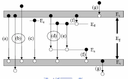
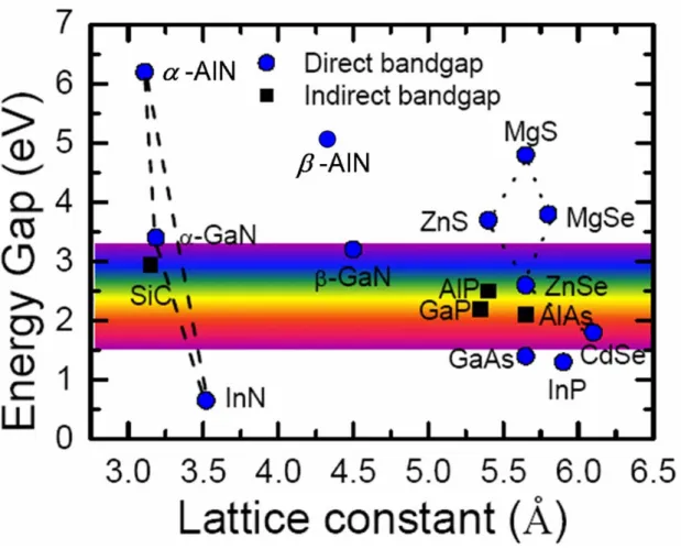
(31) bandgap is required for the emission of photon in order to meet total momentum conservation. In the optical transition process [116], a simplified set of transitions in semiconductor is shown in Fig. 2.3. Process (a) is an interband transition; this produces intrinsic luminescence. Although this recombination occurs from states close to corresponding band edges, the thermal distribution of carriers in these states will lead to broad emission spectra. Process (b) is a higher-energy emission involving energetic or hot carriers, sometimes related to avalanche emission. Process (c) is the exciton decay observable at low temperature. Both free-excitons and excitons bound to an impurity may undergo such transitions. Process (d) is a deep transition. Deep transitions involve transitions of the electron from conduction band to an acceptor level or transition form donor level to valence band. Process (e) is a donor-acceptor pair recombination. Process (f) is called a shallow transition. This transition is from the acceptor level to valence band or from the conduction band to donor level. Process (g) is an intraband transition involving hot carriers, sometimes called deceleration emission. As mentioned above, the transition involves radiative and non-radiative recombination. Not all transition can occur in the same material or under the same condition. An efficient luminescence material is one in which radiative transitions predominate over nonradiative ones. Figure 2.4 shows the energy gap versus the. 13.
(32) lattice constant for several compound semiconductors [117]. For AlN, both wurtzite and zincblende structures are direct bandgap semiconductors, and the band gaps are about 6.2 eV and 5.0 eV, respectively [118].. FIG. 2.2 Energy diagram of (a) direct- and (b) indirect-gap semiconductors. [112,116]. 14.
(33) FIG. 2.3 Schematic diagram of transitions in a semiconductor. Ec is the conduction band, Ev the valence band, Ee the exciton level, Ed the donor level, and Ea the acceptor level. [112,116]. 15.
(34) FIG. 2.4 Energy gap of different compound semiconductors as a function of lattice constant. [112,117]. 16.
(35) 2.3 Raman spectroscopy Vibrational transition can be observed in IR (infrared) or Raman spectra. Figure 2.5 shows differences in mechanism of Raman and IR. According to quantum mechanics [119], a vibration is IR-active if the dipole moment is changed during the vibration, and is Raman-active if the polarizability is changed during the vibration. In IR spectroscopy, a molecule absorbs energy ν=∆hE from IR source at vibrational transition. The intensity of absorption is governed by Beer-Lambert law:. I = I 0 e −α d. (2.3.1). where I and I0 are the intensities of incident and transmitted light, respectively. α is the molecular absorption coefficient [120], and d is the sample thickness. The percentage of transmittance T(%) is given as. T (%) =. I × 100 I0. (2.3.2). The absorbance (A) is defined as. A = log. I = αd I0. (2.3.3). The IR spectroscopy often plots percentage transmittance T(%) or absorbance A with respect to the wavenumber to obtain the molecular vibrational modes.. 17.
(36) FIG. 2.5 Mechanism of (a) IR, and (b) Raman spectroscopy. [112,119]. 18.
(37) In Raman spectroscopy, an intensive laser with linear polarization is often used as the excitation source. According to the classical theory, Raman scattering can be explained in the following. The oscillating electric field strength (E) of an electromagnetic wave is given by E = E0 cos 2πν 0t. (2.3.4). where E0 is the amplitude of electric field and ν0 is frequency of incident laser. If a diatomic molecule is irradiated by the laser, an electric dipole moment P is induced: P = αE = αE0 cos 2πν 0t. (2.3.5). where α is the polarizability of the molecule. In general, α is a 3 x 3 matrix. In the Cartesian coordinates, ⎡ Px ⎤ ⎡α xx α xy α xz ⎤ ⎡ E x ⎤ ⎥⎢ ⎥ ⎢ P ⎥ = ⎢α ⎢ y ⎥ ⎢ yx α yy α yz ⎥ ⎢ E y ⎥ ⎢⎣ Pz ⎥⎦ ⎢⎣α zx α zy α zz ⎥⎦ ⎢⎣ E z ⎥⎦. (2.3.6). The matrix, α, is called the polarizability tensor. In normal Raman scattering,. α xy = α yx , α xz = α zx , and α yz = α zy . The vibration is Raman-active if one of these components of the polarizabilty tensor is changed during the vibration. If the vibrational frequency of the molecule is ν , the nuclear displacement q is given by m. q = q0 cos 2πν m t. (2.3.7). where q0 is the vibrational amplitude. For a small vibration, α can be expanded in terms of q as. 19.
(38) ⎛ ∂α ⎞ ⎟⎟ q + .... ⎝ ∂q ⎠0. α = α 0 + ⎜⎜. (2.3.8). ⎛ ∂α ⎞ ⎟⎟ is the rate of change of α Here, α0 is the polarizability at equilibrium position ⎜⎜ ∂ q ⎝ ⎠0 with respect to the change in q evaluated at the equilibrium position. Substituting Eqs. 2.3.4, 2.3.7 and 2.3.8 into Eq. 2.3.5, Eq. 2.3.5 becomes. P = αE0 cos 2πν 0 t ⎛ ∂α ⎞ ⎟⎟ q0 E0 cos 2πν 0 t cos 2πν m t + ... = α 0 E0 cos 2πν 0 t + ⎜⎜ ⎝ ∂q ⎠ 0. (2.3.9). 1 ⎛ ∂α ⎞ ⎟ q0 E0 [cos{2π (ν 0 −ν m )t}+ cos{2π (ν 0 + ν m )t}] + .. = α 0 E0 cos 2πν 0 t + ⎜⎜ 2 ⎝ ∂q ⎟⎠ 0 The first term in Eq. 2.3.9 represents an oscillating dipole that radiates light of frequency ν0, which is called Rayleigh scattering. The ν0 – νm and ν0 + νm in the second term are called Stokes and anti-Stokes Raman lines, respectively. It should be ⎛ ∂α ⎞ ⎟⎟ is zero, the vibration is not Raman-active. In other words, to be noticed that if ⎜⎜ ⎝ ∂q ⎠0 Raman-active, the rate of change of polarizability with the vibration must not be zero. A simple diagram vibrational transitions is illustrated is Fig. 2.6 [121]. In IR spectroscopy, only transition of ν = 0 (vibrational ground state) → 1 (vibrational first excited state) at the electronic ground state can be observed. For normal Raman spectroscopy, an exciting laser energy ν0 is chosen so that its energy is far below the first excited state. The virtual states are plotted as dotted lines to distinguish the real excited state. According to the Maxwell-Boltzmann distribution law, the population 20.
(39) ratio of the ν = 1(Pν =1 ) and ν = 0(Pν = 0 ) states is given by − ∆E. Pν =1 = e κT Pν =0. (2.3.10). where ∆E is the energy difference between two states, T is the absolute temperature, -23. and k is Boltzmann’s constant (1.38 x 10. Joule/degree). In general, the population of. molecules at ν = 0 is much larger than that ν = 1. Thus, the Stokes lines (S) are stronger than the anti-Stokes (A) lines under normal condition. Resonance Raman (RR) scattering occurs when the exciting line is chosen so that its energy intercepts the manifold of an electronic excited state. Finally, the fluorescence spectra are observed when the excited state decays to the lowest vibrational state via radiationless transitions and then emits radiation.. ( ). AlN normally has a wurtzite structure with the space group of P63 mc C64ν . The wurtzite structure consists of alternating biatomic close-packed (0001) planes of Al and N pairs stacked in an ABABAB sequence. Figure 2.7 shows the views of wurtzite AlN along [0001] , [1120] , and [1010] directions [122]. The zincblende structure of AlN belongs to space group of F 43m(Td2 ) . The stacking sequence for the (111) close-packed planes in this structure is ABCABC. Views of the zincblende structure are shown in Fig. 2.8 [122].. 21.
(40) FIG. 2.6 Energy levels of IR, normal Raman, resonance Raman, and fluorescence spectra. R: Rayleigh scattering, S: Stokes Raman scattering, A: anti-Stokes Raman scattering. [112,121]. 22.
(41) FIG. 2.7 Crystal structure views of wurtzite along different directions: (a) [0001], (b). [1120] , and (c) [1010] .[112,122]. FIG. 2.8 Crystal structure views of zincblende along different directions: (a) [100], (b) [110], and (c) [111].[112,122]. 23.
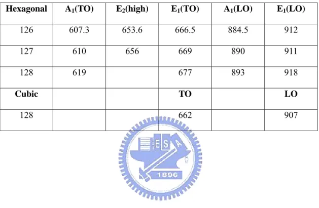
(42) The first-order Raman scattering is caused by the phonon with a wavevector near Γ point (k = 0), because the light scattering process must follow the momentum conservation rule. According to the group theory selection rule, zincblende-type materials have a doubly degenerate TO and a single LO phonon modes close to k = 0. The wurtzite-type crystal structure has eight sets of phonon modes at the Γ point namely 2A1 + 2E1 + 2E2 + 2B1. A1 and E1 modes are acoustic phonon modes. The remained six modes of A1 + E1 + 2E2 + 2B1 are optical phonon modes. Figure 2.9 shows an atomic displacement scheme of these optical phonon modes. Atomic displacements in A1 and B1 modes are along the c-axis, while the atomic displacements in E1 and E2 modes are give perpendicular to the c-axis. The A1 and E1 modes are both Raman and IR active, while the two E2 modes are only Raman-active, and the two B1 modes are silent modes of Raman and IR [123-125]. Typical wurtzite- and zincblende-AlN phonon modes are summarized in Table 2.1 [126-128].. 24.
(43) FIG. 2.9 Optical phonon modes in wurtzite structure. [112]. 25.
(44) Table 2.1 Typical phonon frequencies in hexagonal and cubic AlN obtained by Raman spectroscopy at room temperature.. Hexagonal. A1(TO). E2(high). E1(TO). A1(LO). E1(LO). 126. 607.3. 653.6. 666.5. 884.5. 912. 127. 610. 656. 669. 890. 911. 128. 619. 677. 893. 918. Cubic. TO. LO. 128. 662. 907. 26.
(45) 2.4 Field Emission 2.4.1 Field Emission from metal Field emission is a quantum-mechanical phenomenon in which electrons tunnel through a potential barrier at the surface of a solid as a result of the application of a large electric field. Field emission is distinct from thermionic emission and photoemission in which electrons acquire sufficient energy via heating or energy exchange with photons, respectively, to overcome the potential barrier. In field emission external electric fields on the order of 107 V•cm-1 are required for appreciable electron currents. The presence of the electric field makes the width of the potential barrier being finite, and therefore permeable to the electrons. This can be seen with the Fig. 2.10 [129], which presents a diagram of the electron potential energy at the surface of a metal. The dashed line in Fig. 2.10 shows the shape of the barrier in the absence of an external electric field. The height of the barrier is equal to the work function of the metal, φ, which is defined as the energy required to remove an electron from the Fermi level EF of the metal to a rest position just outside the material (the vacuum level). The solid line in Fig. 2.10 corresponds to the shape of the barrier in the presence of the external electric field. As can be seen, in addition to the barrier becoming triangular in shape, the height of the barrier in the presence of the electric field E is smaller, with the lowering given by Eq.( 2.4.1) [130].. 27.
(46) ⎛ eE ∆ φ = ⎜⎜ ⎝ 4 πε. o. ⎞1/ 2 ⎟⎟ ⎠. (2.4.1). where e is the elementary charge and εo is the permittivity of vacuum. Knowing the shape of the energy barrier, one can calculate the probability of an electron with a given energy tunneling through the barrier. Integrating the probability function multiplied by an electron supply function in the available range of electron energies leads to an expression for the tunneling current density J as a function of the external electric field E. The tunneling current density can be expressed by Eq. (2.4.2) which is often referred to as the Fowler-Nordheitn equation [131]. ⎡ − 8π (2 m )1 / 2φ 3 / 2 ⎤ e 3E 2 ( ) J= exp v y ⎢ ⎥ 2 3heE 8πhφt ( y ) ⎣ ⎦. (2.4.2). where y= ∆φ/φ with ∆φ given by Eq. (1), h is the Planck's constant, m is the electron mass, and t(y) and v(y) are the Nordheim elliptic functions; to the first approximation t2(y)= 1.l. and v(y) = 0.95 – y2. Substituting these approximations in Eq. (2.4.2),. together with Eq. (2.4.1) for y and values for the fundamental constants, one obtains Eq. (2.4.3) [131]. −6. J = 1.42 × 10. ⎛ − 6.44 × 10⁷φ 3 / 2 ⎞ ⎛ 10.4 ⎞ ⎟⎟ exp⎜⎜ 1/ 2 ⎟⎟ exp⎜⎜ φ E ⎝φ ⎠ ⎝ ⎠. E2. (2.4.3). where J is in units of A cm-2, E is in units of V cm-1and φ in units of eV. Plotting log (J/E2) vs. 1/E results in a straight line with the slope proportional to the work function value, φ , to the 3/2 power. Eq. (2.4.3) applies strictly to temperature equal to 0 K. 28.
(47) However, it can be shown that the error involved in the use of the equation for moderate temperatures (∼300 K) is negligible.. Fig. 2.10 Diagram of potential energy of electrons at the surface of metal. [129]. 29.
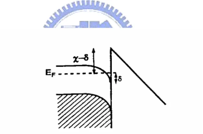
(48) 2.4.2 Field Emission from Semiconductor To a large degree, the theory for electron emission from semiconductors can be derived parallel to the theory for metals. However, special effects are associated with semiconductors due to the state of their surface and the fact that an external field applied to a semiconductor may penetrate to a significant distance into the interior. The classic theoretical treatment of electron emission from semiconductors is given in. For the case when the external electric field penetrates into the interior of an n-type semiconductor and the surface states are neglected, log(J/E2) is shown to be a linear function of 1/E, as for metals. However, in place of the work function φ in the Fowler-Nordheim equation one needs to substitute a quantity χ - δ, where χ is the electron affinity defined as the energy required for removing an electron from the bottom of the conduction band of the semiconductor to a rest position in the vacuum, and δ denotes the band bending below the Fermi level. These parameters are illustrated in Fig. 2.11 [129]. The linear dependence of log (J/E2) on 1/E is expected only if the density of the current flowing through the sample is much smaller than the current limiting density Jlim = enµnE/ε, where µn is the electron mobility and n is the electron concentration in the bulk of the semiconductor [132,133]. At J≈ Jlim the Fowler-Nordheim character of the relationship J(E) passes into the Ohm's law (if the dependence of electron mobility. 30.
(49) on the electric field is neglected) which results in the appearance of the saturation region in the emission current vs. voltage curve. Such saturation regions were observed experimentally for lightly doped n-type semiconductors and for p-type semiconductors [134,135]. Electron emission from semiconductors has been a subject of more recent theoretical considerations, which takes into account complications due to electron scattering, surface state density, temperature, and tip curvature [136,137].. Fig. 2.11 Diagram of potential energy of electrons at the surface of an n-type semiconductor with field penetration into semiconductor interior. [129]. 31.
(50) Chapter 3 Experimental method. 3.1. Experimental Details Starting substrates were mirror-polish, (100) oriented wafer, differently doped, including p+-type (boron doping, resistivity ~ 2-5 mΩ cm), p-type (boron doping, resistivity ~ 10 Ω cm), n-type (phosphor doping, resistivity ~ 10 Ω cm), and n+-type (phosphor doping, resistivity ~ 2-5 mΩ cm) silicon substrates. After the pre-treatment of substrates, they were put into a commercial plasma metal coater to deposit the metal layer. Then, the metal-coated (Au, Pt, Al) Si substrates were placed into the atmospheric pressure chemical vapor deposition (APCVD) system to prepare AlN nanomaterials with various deposition parameters. Finally, several apparatuses were used to analyze the characterization of these nanomaterials.. 3.2. Atmospheric pressure chemical vapor deposition Figure 3.1 schematically depicts the layout of the APCVD system [99,106,138]. The AlNNTs were grown by vapor transport and condensation process using silicon substrates covered with gold, platinum or aluminum that act as catalysts. An aluminum oxide boat, carrying the metal coated silicon substrate and pure aluminum 32.
(51) powders (SHOWA, Japan), was placed inside a quartz tube (1 inch in diameter). The Al powders were kept up stream and the Au-coated Si substrate was placed upside down (Au-coated side facing the Al powders) and downstream with respect to the flow of the nitriding gas, in this case NH3. The quartz tube was housed in a conventional tube furnace. The quartz tube was degassed and then purged with ammonia NH3 (30 sccm) as the atomic nitrogen precursors. During the growth process, the furnace was ramped up to 950, 1000, 1100, and 1200°C, respectively, and held at that temperature for 30 mins with an ammonia flow rate of 30 sccm. After cooling down, the products collected on the silicon substrate were characterized by high-resolution SEM analysis, and the structure of the nanotips was studied using a high resolution transmission electron microscope (HRTEM), XRD and Micro-Raman.. 33.
(52) FIG. 3.1 Schematic diagram of the atmospheric pressure chemical vapor deposition. 34.
(53) 3.3 Characterization of AlN nanomaterials 3.3.1. Scanning electron microscopy (SEM) The scanning electron microscopy (SEM) was used the secondary electron mode to observe the morphology of AlN nanomaterials. The model of the SEM used here is JEOL JSM6700F. 3.3.2. Transmission electron microscopy (TEM) One of the typical characters of nano-phase materials is the small object size. Although some structural features can be revealed by x-ray and neutron diffraction, direct imaging of nanomaterials is only possible using high resolution transmission electron microscopy (HRTEM, Philips TECNAI 20). TEM is a unique technique because it can produce a real space image on the atom distribution in the nanocrystal surface. With a finely focused electron probe, the structural characteristic of a single nanomaterial can be fully understood. Normally, the chemical analysis system, the energy disperse X-ray spectrometer (EDX), was attached on TEM system. 3.3.3. Electron energy loss spectroscopy (EELS) EELS is a nano-analytical technique that uses the characteristic spectrum of energy losses of transmitted electrons to obtain information about elemental composition, chemical bonding, and electronic structure [139,140]. An EELS spectrum consists of a monotonically-decreasing background on which several broad. 35.
(54) peaks, each characteristic of a particular inelastic scattering process, are superimposed. The spatial resolution is limited by the diameter of the incident illumination focused on the sample. The energy loss spectrum displays the intensity distribution of the imaging electrons as a function of the energy loss. It supplies qualitative and quantitative information about the atomic and molecular structure of this specimen.. 3.3.4. X-ray diffraction spectroscopy X-ray diffraction analysis of the AlN nanomaterials specimens was carried out by using a Rigaku D/max diffractometer using θ/2θ mode. The X-ray was generated by a Cu target (Cu Kα) operated at 40 kV and 100 mA, and the scanning speed was 0.02 deg/step, 1deg/min from 20° to 75°. The silicon signal was used to calibrate the diffraction patterns. 3.3.5. Micro-Raman spectroscopy Raman spectroscopy is an excellent technique for characterization of the crystalline quality either in films or nanostructures. The various products were qualitatively analyzed by laser micro-Raman spectroscopy (Renishaw Raman Microscope, Model 2000). In the Raman experiment, an Nd-YAG laser excitation with the wavelength of 532.2 nm was used as an exciting light source. The laser light with the power of 500 mW was reflected by a half-mirror, and focused on to the sample with an objective lens. The operational region can be conducted from 150~8000 cm-1 with the. 36.
(55) resolution of 1~5 cm-1. 3.3.6. Cathodoluminescence (CL) Cathodoluminescence is the light emission associated with the excitation of materials by an electron beam. The optics of a scanning electron microscope can be utilized to produce a focused beam and to excite a small region of the sample. The beam diameter in the SEM is of the order of a few nanometers. The excited volume depends on the energy of the electron beam. Electron energies ranging from 0.1 keV to 20 keV are commonly used in the SEM. The resulting probe volumes range from tens of nanometers to a few microns in radius. The light emitted from such region is captured by a parabolic mirror, and a spectrum is obtained using a grating and a high efficiency light detector. By changing the energy of the electron beam it is possible to perform a depth profile of the optical properties of the specimen. By scanning in the form of a raster, it is possible to produce images of the light emitting intensities for specific wavelengths. The resolution of the technique depends on the diffusion length of the excited carriers. It can be as small as the electron probe in the case of very small diffusion lengths. Temperature-dependent CL study was performed using a Gatan MonoCL3 system with an accelerating voltage of 15 kV, current density of electron beam of 20 mA attached to a JEOL JSM-6700F field emission scanning electron microscope. The photomultiplier is biased at -1500 volt. The scanning rate. 37.
(56) was kept at 1 nm/ step with each step dwell for one second. 3.3.7. Photoluminescence (PL) The photoluminescence and photoluminescence excitation properties of AlN nanomaterials were measured by a Tau-3 lifetime system. The light source is a Xe lamp with power of 450 W. The excitation area is ranging from 2.06 to 5.65 eV, and emission area is ranging 1.46 to 4.13 eV with a high resolution of 0.4 meV. The tau-3 lifetime system has two mode of operation: one is steady-state mode, the other is lifetime (kinetic) mode. The life-time range can be conducted from 10 pico-second to 10 micro-seconds. 3.3.8. Thermoluminescence (TL) Thermoluminescence (TL) is the process in which a material emits light while it is being heated [141-143]. The light emitted is due to the recombination of charges trapped at metastable defect sites within the material lattice, and its amount is proportional to energy absorbed by the mineral as a result of its previous exposure to ionizing radiation. However, TL is totally different from the incandescence, which is emitting light due to high temperature of the solid. Normally, charges trapped in deep traps in a material's lattice will remain there indefinitely if the material rests at the ambient temperature. However, heating a material to such a specific temperature immediately evicts trapped electrons from the. 38.
(57) deep traps. They promptly undergo recombination, and in doing so emit photons in the visible spectrum. The amount of light emitted is proportional to the material’s intrinsic sensitivity to radiation and the total amount of radiation energy absorbed. Comparisons made of the light emitted by a natural sample and the amount of light emitted by a sample with a known added radiation dose, plus separate dosimetry measurements, allow the sample's age since it was last exposed to a clock-resetting event to be calculated. First, samples were irradiated by UV light through an UV lamp with interference filters. The UV irradiation locks the electrons into the defects. When the electrons are induced to leave the lattice, there is an emission of luminescent light. TL measurement was made using a Risø model TL reader with linear planchet heating and equipped with a built-in 90Y/90Sr software-controlled beta source. 3.3.9. UV absorption UV absorption was done in Model U-3010 (Hitachi, Japan) spectrophotometer covers the UV/Visible range from 190-900 nm by employing both a tungsten-iodide (WI) lamp for the visible region and a deuterium (D2) lamp for the ultraviolet region. 3.3.10. Measurement of field emission characterization The turn-on field for 10 µA/cm2 has been used as the merit parameters to distinguish various emitter materials [144-146]. Field emission properties were. 39.
(58) measured by using diode-type structure. An anode plate (ITO Glass) was placed at 70 μm above the AlN nanomaterials emitters, which served as the cathode electrode. The field emission (FE) measurement was carried out in a vacuum chamber at a pressure of ~10-7 torr at room temperature. The applied voltage was biased from 0 to 1100 V and current which was collected from the emitters was recorded by using a Keithley 237 system.. 40.
(59) Chapter 4 Growth of AlN nanotips by means of APCVD. In this chapter, preparations of AlN nanotips (AlNNTs) on the Si (100) substrates by APCVD method will be presented. The effects of the thickness of catalyst, type of catalysts, and preparation time on the formation of single-crystalline AlN in the CVD experiments are studied. The surface morphology, structure, and composition properties of the as-deposited samples are characterized in detail. The overall structural and morphological results are discussed in section 4.2 via FESEM Raman scattering and XRD measurements, respectively. The growth mechanism of AlNNTs formation was described in section 4.3. Finally, section 4.4 will make a summary according to the obtained results.. 4.1. AlN nanotips growth AlN nanowires, whiskers and nanotubes have been obtained by chloride assisted growth [115,116], arc process [117], carbothermal reduction [118,119], and gas-reduction-nitridation [120]. However, very recently, there has been an increased activity in this field with quite a few reports on nanowires, nanotubes and nanobelts decorating the 1D AlN domain. Vapour-liquid-solid (VLS) growth of hexagonal AlN. 41.
(60) nanowires and nanotubes with [001] growth direction have been reported at temperatures above 1100°C [121,122]. Hexagonal AlN nanobelts with rectangular cross-section and having [001] growth direction also made their appearance [123]. Vapor-solid (VS) growth is a vapor species directly transformed into solid nanowire process [124]. The VS process does not need catalyst to assist the nanowire growth. Therefore, it does not undergo a liquid-alloy stage. A cubic AlN nanotube with a boron nitride (BN) wrapping (AlN-BN composite nanotube) has been made possible at a temperature of 1200°C using a two stage growth mechanism [125]. However, AlN nanotips with high aspect ratio, unlike the pyramids [126], also form a special class in the 1D family, have not been reported before. Nanotips in Si-based and other more conventional semiconductor systems have been demonstrated and explored for various potential applications as field-emitters [146-148], solar cells [149], bio/chemical sensing devices [150-152], and optical nanodevices [36,153]. Until now, optical lithography has been playing the major role in fabricating sharp tips but limited to 50 nm in radius [154-156]. A novel electron-cyclotron-resonance plasma assisted dry-etching technique has recently been developed for producing ultra-fine tips (~ 1 nm) in a wide range of material systems, excluding AlN [157]. These tips (Si, poly-Si, GaN, GaP, Al) can have apex diameters from 2-20 nm, and growth directions depending upon the orientation of the starting. 42.
(61) wafers. The approaches captioned above can be classified as top-down techniques and are most suitable for plate or wafer process. In this study, we report on the first synthesis of single-crystalline AlNNTs with a monodispersed angle distribution via simple vapor transport and condensation process (VTCP), in both catalytic and catalyst-free modes, at 950 °C, which is significantly lower than that of the conventional carbothermal reduction and nitridation process for AlN. Metal (Au, Pt, Al) coated silicon (Si) substrates have been used to produce the AlNNTs, where the metal nanoparticulates formed at the high temperature acted as the nucleation sites for the AlNNTs growth.. 4.2 Results and discussion The as-grown AlNNTs on silicon substrates coated with an Au layer of various thicknesses were shown in Fig. 4.1a-c. AlNNTs grown on a 7 nm Au covered Si substrate exhibited a mean diameter of 10 nm at the apex, 80 nm at the base, and 250 nm in length (Fig. 4.1a). AlNNTs grown with progressively thicker Au layers produced longer nanotips (300-3000 nm) with wider apex (20-100 nm) and base (100-700 nm) diameters (Fig. 4.1b-c). Typical cross-sectional SEM image of AlNNTs is shown in Fig. 4.1d. This image displays a high density of quasi-aligned AlNNTs uniformly distributed over the entire substrate. The tip like morphology suggests that. 43.
(62) the growth rate of the AlNNTs along the axial direction far outpace the growth rate along the radial direction. Along with the AlNNTs containing pure Al nanocrystals at its base some unreacted metallic Al residue could be found. The beauty of this VTCP technique lies in the size control of the nanotips which can be simply achieved by adjusting the thickness of the gold layer keeping the other growth parameters such as temperature and gas flow rates fixed. However, a number of other metals, such as aluminum (Al) (Fig. 4.2a) or platinum (Pt) (Fig. 4.2b), can be used to produce the AlNNTs since the eutectic temperatures of these metals with silicon lie below the reaction temperature of 950 °C. Furthermore, AlNNTs can be grown on even bare Si (without metal coating) (Fig. 4.2c) but they exhibit relatively poor morphology, indicating that metal coating is not indispensable for the growth, but it does help in controlling the morphology of the AlNNTs and perhaps some increase in the yield. But to come to any such conclusion, a closer look at the initial stages of growth was deemed necessary. SEM images in Fig. 4.3a-c demonstrate the initial growth of AlNNTs. The Al nanocrystals form within the first 20 minutes of growth and can be easily seen at the base of the AlNNTs (Fig. 4.3a). Figure 4.3b and 3c represent the morphology during the first 20 and 25 minute of growth, respectively, with typical nanotip formation completed in 25-30 minutes. The corresponding energy dispersive X-ray spectroscopy (EDS) elemental analysis of the nanotip body and nanoparticles. 44.
(63) lying at the base of the nanotip is shown in Fig. 4.3d. It is quite clear that the nanotip body showed a much pronounced nitrogen component whereas no Au signal could be obtained from the apex of such tips marked (A) in Fig. 4.3c which excludes the possibility of VLS growth mechanism. The crystallites lying at the base of the nanotips, marked (B) in Fig. 4.3c, from which the nanotips evolved, yielded signals predominantly from Al, Au, and Si with no or little nitrogen component (Fig. 4.3d). The carbon and copper signals in Fig. 4.3d come from the amorphous carbon coated copper grids used for the TEM measurements. Two interesting inferences can be drawn from Fig. 4.3d. First, the nanocrystal at the base is predominantly Al, and second, the Al at the tip is compounded with nitrogen. Both of these facts will be corroborated from the XRD results to be discussed later. However, the establishment of the AlN phase in the nanotips comes conclusively from the TEM and XRD results. Presence of Au along with Al in the nucleating crystallites only, indicates that either pure gold or a gold silicide phase may be controlling the nucleation and the smooth and finer morphology of the AlNNTs. In fact, the thickness of the Au layer is the key to the resultant morphology of the AlNNTs (Fig. 4.1). Au redundancy during growth resulted in larger and corrugated edge morphology of the AlNNTs (Fig. 4.2c). The fact that AlNNTs can be grown on bare silicon (Fig. 4.2c) as well as on silicon covered with Al (Fig. 4.2a) indicates that a self catalytic role of pure aluminum. 45.
(64) nanocrystals, cannot be ruled out. Al vapors condense as crystalline Al on the catalytic gold or the gold-silicide sites, and we believe that these crystallized Al nanoparticles present at the bases of the AlNNTs served as the nucleation sites for subsequent AlNNTs growth following deposition of reacted Al and N vapors.. 46.
(65) FIG. 4.1 Typical SEM images of the AlN nanotips grown with (a) 7 nm, (b) 15 nm, and (c) 50 nm thick Au layer on Si. (d) Typical cross section SEM image of AlN nanotips grown with 15 nm Au coated Si substrate.. 47.
(66) FIG.. 4.2 SEM images of AlN nanotips grown with (a) Al (15 nm), (b) Pt (15 nm), (c) no metal coating, on the Si substrate, respectively.. 48.
(67) FIG. 4.3 SEM images of AlN nanotips grown with Au (15 nm on Si) for (a) 15 min, (b) 20 min, (c) 25 min, and (d) the corresponding TEM-EDS spectra of the AlN nanotip and nanoparticle marked (A) and (B) in Fig. 4.3c.. 49.
(68) In order to investigate the structure evolution of the AlNNTs, XRD analyses were performed at various stages of growth. As shown in Fig. 4.4a, the XRD data for the initial stage shows the presence of Al only whereas the corresponding data for the later stage shows a number of relatively sharp diffraction peaks that can be indexed to a hexagonal structure with lattice constant of a = 0.311 nm and c = 0.498 nm, which is consistent with the standard value for bulk hexagonal AlN (JCPDS 25-1133). While there are negligible signals from Au, the Al signals remain detectable in the XRD spectra, presumably due to the un-reacted aluminum crystallizing on the Au particles at the base of the AlNNTs during the initial high temperature processing of the reactants. It should be noted that all samples showed similar XRD patterns, indicating that the nanotips have good structural reproducibility in all deposition conditions used. This kind of reproducibility is a pre-requisite for any synthetic technique to be accepted as a major force. Raman spectra of the AlNNTs were obtained at room temperature as shown in Fig. 4.4b, to further the knowledge of its structure. In this spectrum, distinct first-order modes of the peaks corresponding to A1 (TO), E2 (high), E1 (TO) and A1(LO) modes at around 609.4, 653, 668 and 894 cm-1, respectively, were observed. These Raman peaks are signatures for wurtize AlN as reported previously for bulk, thin film, nanowires, and nanobelt structures [126,127,158-159]. However, these peak. 50.
(69) positions were given alternative assignments in an earlier work [160]. These Raman peaks were not detected from the samples containing predominantly nanocrystals (such as those grown for 15 min or less as shown in Fig. 4.3a), suggesting that AlN signal is indeed originating from the well crystallized tips.. FIG. 4.4 (a) Typical XRD spectra taken at three different stages of growth. The initial stage shows only Al signals and the corresponding one with fully grown nanotips shows two crystalline phases of Al and hexagonal AlN. (b) Raman spectrum, with a discontinuous abscissa, of the AlN nanotips on silicon substrate. Inset shows a continuous Raman spectrum of the AlN nanotips with the silicon signal included. All the XRD and Raman spectra were measured from samples prepared on 15 nm Au coated Si substrate.. 51.
(70) High resolution TEM along with the selected-area electron diffraction (SAED) was employed to further analyze the structure and crystallographic orientations of these AlNNTs. All nanotips appear to be homogeneous without any grain boundaries, indicating the single crystal nature of each individual AlNNT. As shown in Fig. 4.5b, the HRTEM image of the apex reveals a lattice spacing of 0.497 and 0.269 nm (in parallel and normal to the axial direction) that is in good agreement with the d001 and d1-10 spacing of h-AlN, respectively. Corroborating with the SAED pattern, the direction of the AlNNTs was found to be [001] along the long axis (inset, Fig. 4.5b). −. −. −. AlN whiskers growing along {10 1 0} and { 1 2 1 0} close packed planes have already been reported [161], and [001] growth direction of some 1 dimensional nanostructures was also observed [159,162]. HR-TEM examination and SAED performed over several nanotips made from different thickness of gold films and also at different locations on each nanotips yielded similar diffraction patterns. Elemental analysis on a single AlNNT body (Fig. 4.5c) done by electron energy loss spectroscopy (EELS) measurements clearly established a stoichiometric AlN composition with Al (Fig. 4.5d) and N (Fig. 4.5e) mapped with similar rate of occurrence.. 52.
(71) FIG. 4.5 (a) TEM image of an AlN nanotip, (b) High resolution TEM image of a single AlN nanotip with clear lattice images. The inset shows a SAED pattern of the nanotip indicating the single-crystalline nature with [110] zone axis and the growth direction along [001]. (c) TEM of a single AlN nanotip with corresponding (d) Al, and (e) N mapping using EELS.. 53.
數據
![FIG. 2.1 Schematic diagram of VLS growth mechanism. The nanowire growth includes three stages of (a) alloying, (b) nucleation, and (c) axial growth [108,112]](https://thumb-ap.123doks.com/thumbv2/9libinfo/8029935.161358/28.892.144.745.353.716/schematic-diagram-mechanism-nanowire-includes-alloying-nucleation-growth.webp)

+7
![FIG. 2.8 Crystal structure views of zincblende along different directions: (a) [100], (b)](https://thumb-ap.123doks.com/thumbv2/9libinfo/8029935.161358/41.892.165.708.548.955/fig-crystal-structure-views-zincblende-different-directions-b.webp)
![FIG. 2.9 Optical phonon modes in wurtzite structure. [112]](https://thumb-ap.123doks.com/thumbv2/9libinfo/8029935.161358/43.892.223.674.207.836/fig-optical-phonon-modes-wurtzite-structure.webp)
![Fig. 2.10 Diagram of potential energy of electrons at the surface of metal. [129]](https://thumb-ap.123doks.com/thumbv2/9libinfo/8029935.161358/47.892.167.718.371.720/fig-diagram-potential-energy-electrons-surface-metal.webp)

相關文件
Creating full view panoramic image mosaics and texture-mapped models, SIGGRAPH 1997, pp251-258. Lowe, Recognising Panoramas,
• Description “pauses” story time while using plot time; there can be a nearly complete distinction between the forms of time.. • Ellipsis skips forward in story time while
Visa Application Denied Stamp - Image courtesy of Stuart Miles / FreeDigitalPhotos.net Visa Application Approved Stamp - Image courtesy of Stuart Miles / FreeDigitalPhotos.net
Light rays start from pixels B(s, t) in the background image, interact with the foreground object and finally reach pixel C(x, y) in the recorded image plane. The goal of environment
• Concept of High Conflict Complainants, their characteristics and relationship with Personality Disorders.. • Tips in handling High Conflict
match fundamental
Keywords: Corporate Social Responsibility (CSR), brand image, product attributes, purchase intention, Structural Equation Models (SEM)... 誌
X-ray diffractograms of liquid crystalline polymers.... TGA results of polymers
