1336 IEEE TRANSACTIONS ON ELECTRON DEVICES, VOL. 36. NO. 7, JULY 1989
A
New Criterion for Transient Latchup Analysis
in
Bulk
CMOS
Abstract-This paper describes a new criterion for transient latchup of p-n-p-n structures initiated by current pulses. Based upon the cir- cuit-oriented model, the terminal currents and voltages of the transis- tors as a function of the pulsed triggering currents are characterized, and the charge storage within p-n-p-n structures is investigated. It is found that, to maintain the regeneration process, the change of charge stored in junction depletion capacitances of a p-n-p-n structure must be greater than a certain value independent of the triggering currents. Thus, the new criterion is constructed in terms of the constant charge storage within a p-n-p-n structure. Applying the criterion, latchup im- munity against pulsed triggering currents can be evaluated with re- spect to process and device parameters. Both SPICE simulations and experimental results confirm the validity of the proposed transient cri- terion. It is found that large transit time of bipolar transistors and large well-substrate junction depletion capacitance lead to higher latchup immunity against pulsed triggering currents.
NOMENCLATURE Collector junction capacitance. Emitter junction capacitance.
Low-current compensation parameter of a bipo- Reverse saturation current of a bipolar transistor. Regeneration time of a p-n-p-n structure. Thermal voltage.
Ideal maximum forward (reverse) current gain of Forward (reverse) transit time of a bipolar tran- High-level injection parameter of a bipolar tran- Built-in potential of a p-n junction.
Lateral p-n-p transistor. Vertical n-p-n transistor. lar transistor. a bipolar transistor. sistor. sistor. I. INTRODUCTION
T is known that one of the main factors limiting the
I
performance of VLSI CMOS circuits is latchup phe- nomenon, i.e., the triggering operation of parasitic p-n-p-n structures. According to either the holding-point[ 11-[4] or triggering-point [ 5 ] , [6] approach, a number of design models and simulation programs have been pro- posed to analyze the static latchup characteristics. In ad- dition to those static models, a few models are devoted to
Manuscript received September 20, 1988; revised December 20, 1988. The review of this paper was arranged by Associate Editor R. R. Troutman. The authors are with the Institute of Electronics, National Chiao Tung University, Hsin-Chu, Taiwan, Republic of China.
IEEE Log Number 8927655.
characterizing the transient latchup behavior by two-di- mensional numerical simulation or analytic modeling [7]- [ 1 11. Although 2-D transient simulations provide a more accurate analysis of latchup behavior, the rigorous cal- culations generally consume rather large computer time. Moreover, the lack of latchup criterion in 2-D simulation usually leads to a trial-and-error analysis in obtaining the triggering margin of a p-n-p-n structure. Therefore, defi- nite criteria for latchup initiation in the transient case are required to make latchup analysis more meaningful.
Power-up ramp induced latchup has been analyzed [9], and it is shown that the well-substrate junction capaci- tance is important for understanding the power-up tran- sient. On the other hand, an analytic model and transient criterion have been constructed in terms of transistor cur- rents by Goto et al. [lo]. However, using a piecewise linear model and neglecting junction and diffusion capac- itances overestimates the transistor transient currents. Thus, the derived criterion in [lo] is insufficient to accu- rately predict the dynamic triggering behavior of p-n-p-n structures.
In this paper, the transient behavior of p-n-p-n struc- tures under external pulsed triggering currents is investi- gated in detail, and the new criterion for transient latchup initiation is established. Based upon the lumped equiva- lent model, the time-dependent terminal voltages and cur- rents of the parasitic bipolar transistors are first analyzed in Section I1 where the effects of transistor transit time, diffusion capacitances, and bias-dependent junction ca- pacitances are included. Based on the observation of charge storage rather than the variation of terminal cur- rents in the p-n-p-n structures, a dynamic criterion for latchup initiation is proposed in Section 111. From the pro- posed criterion, the relation between the minimum pulse width, or the regeneration time of the p-n-p-n structure, and the pulse height of triggering currents for latchup ini- tiation can be obtained. Comparisons with SPICE simu- lation results confirm the validity of the proposed latchup criterion. Section IV gives the experimental results for various p-n-p-n structures. Good agreement between the experimental and theoretical results is obtained.
11. DYNAMIC BEHAVIOR OF THE p-n-p-n STRUCTURE To simplify the analysis and get an insight into the dy- namic operation, the latchup behavior is characterized through the conventional two-transistor model. Fig. 1
shows the lumped equivalent model for the p-n-p-n struc- 0018-9383/89/0700-1336$01 .OO
0
1989 IEEEYANG A N D WU: NEW CRITERION FOR TRANSIENT LATCHUP ANALYSIS 1337 I K 2 K2 i b l 1c2 Q2 IB2 R1 - -
Fig. I . Lumped equivalent circuit for modeling the transient behavior of the p-n-p-n structure.
ture where, in p-well technology, Q , is the lateral p-n-p transistor and Q 2 is the vertical n-p-n transistor. R I and R2 represent the corresponding well and substrate shunt resistances across the base node of transistors Q 2 and Q , ,
where the pulsed triggering currents Z2 and I , are also ap- plied. Other components are the bias-dependent junc- tion capacitances. Note that the capacitances CJcl and Cjc2 are the well-substrate junction capacitances, which play an important role in transient latchup as will be shown later.
In the transient case, the displacement currents through the junction capacitances and diffusion capacitances of Q ,
and Q2 are so significant that they must be considered. Thus, taking the effects of junction depletion capacitance and diffusion capacitance into consideration, the transient terminal currents of Q , and Q, can be written as [12]
1 , l and lb2 ( 4 ) where ( 5 ) ( 6 ) VEBI / V r CrFI = ( ~ S 1 0 7 F l / W ~ c T R l = ( 1 s l O 7 R l
/
I / T ) e ( V C E ’ + vfBl”vr. andIcl, lBl, Ic2, and I S 2 in (1)-(4) are the static transistor currents of Q , and Q2. These currents are related to the transistor terminal voltages as expressed in Appendix A. The diffusion capacitances C,, and CrR2 have similar expressions to CTFl and CTR1, respectively, which are de- rived by assuming constant transistor transit times 7F, and
T R , ( i = 1, 2 ) . Moreover, the junction depletion capaci- tances C,,, and C,,, ( i = 1, 2 ) in (1)-(4) are also bias dependent and are further expressed in Appendix B .
From the circuit of Fig. 1 , the relations between the terminal currents and voltages can be written as
i c 2 - i b l
+
V,,I/R2+
11 = 0 i,l - ib2 - V B E ~ / R I+
12 = 0 ( 7 ) ( 8 ) VCEI = V B E 2 - VDD (9) and VCE2 = VDD - VEBl ( l o ) Substituting (1)-(4) into (7) and (8), and using (9) and (lo), the dynamic behavior of the base-emitter voltages V E B I and V B E 2 can be obtained asand (12) dVB, I D 2 C l - z D I ( G c I + cjc2) - - - dt ( G c l + C , c 2 ) C F where cl = G c l
+
C j c 2+
q e l
+
CrFI ( 1 3 ) c2 = - ( G C l+
‘JC2+
‘Je2+
‘ 7 F 2 ) ( 1 4 ) ID1 = V E B I / R 2 - - I C 2+
IBl ( 1 5 ) 1 0 2 = 1 8 2+
V B E 2 / R I - IC1 - I 2 ( 16) and ‘F = IeJ‘(+
cTF1)(c,t‘2 + ‘TF2)/(‘JCI + ‘ J C 2 ) - (cjel+
G e 2 + crFl + C r F 2 ) * ( 1 7 )In (13), (14), and (17), the reverse diffusion capacitances
CTRl and C r R 2 are neglected as compared with the junction depletion capacitances
Clcl
and CJc2. Using (1 1) and (12), the variations of V,,, ( t ) and V B E Z ( t ) with respect to both pulsed triggering current II or Z2 and device parameters can be obtained numerically.Fig. 2(a) shows the calculated results of V E B l ( t ) and V B E 2 ( t ) for different pulse widths of II with a fixed pulse height equal to 5 mA. The device parameters used are
1338 IEEE TRANSACTIONS ON ELECTRON DEVICES. VOL. 36, NO. 7, JULY 1989 0.91 I I I
I\
- 0 . 3 L I I 1 2 TIME (ns) (b)Fig. 2 . Variation of VEsl ( 1 ) and VBEZ(r) with different pulse widths of (a) I , and (b) I z applied.
listed in Table I with
RI
= 5.6 kQ and R2 = 800Q.
As can be seen from Fig. 2(a), VEBl increases sharply whenZI
is applied. The sharp increase of VEB, corresponds to a sharp decrease of voltage at the base node of Q,. Thus, due to the capacitive coupling effect caused byCJcl
and C,c2, VBE2 decreases below 0 V during the initial period and thereafter is increased by the increase ofZcl
.
WhenZI
drops to zero at I = 5 ns, VEBl decreases whereas V B E 2
continues to increase for some time (dashed curves), still due to the coupling effect of
C,cl
and CJF2. However, be- cause of the insufficiently large pulse width ofZI
,
the re- generation of the p-n-p-n structure cannot be maintained, and both VEBl and V B E 2 finally decrease to zero, as shown in Fig. 2(a). When the pulse width increases from 5 to 10 ns, the p-n-p-n structure is triggered into latchup, as can be seen from the values of VEB, or V B E 2 (solid curves),which remain at their turn-on value ( = 0.8 V ) after
ZI
is removed.Fig. 2(b) shows the calculated V B E 2 ( t ) and VEBl ( t ) for different pulse widths of Z2 with a fixed pulse height equal to 5 mA. Similarly, an initial delay time is seen for VEB, ( t ) and the pulse width must be sufficiently large to trigger the p-n-p-n structure into latchup.
The variations of terminal currents I,, (
r
), I C , ( t ), ( = VEBl ( t ) / R 2 ) calculated from (Al)-(A4) for the 5-mA pulse height of I , and Z2 are shown in Fig. 3(a) and (b), respectively. We define the regeneration time t, as the re- quired minimum pulse width of a fixed pulse height of ZI or Z2 such that the regeneration process of the p-n-p-n structure can be maintained after I , or Z2 is removed. The value o f t , obtained from SPICE simulations is marked byYANG A N D W U : NEW CRITERION FOR TRANSIENT LATCHUP ANALYSIS Parameter 1, B R I S ( A ) 0 r , ( n s ) 1339 Q1(PNP) B2(NPN) 1.104 211.2 0.2 2.0 2.833E-16 8.112E-16 2.0253-6 1.291E-6 20 0.25 10- 10- 10- n v 4 10-
k
3u
2
10- 10' h -2 v Fig. 3. Variation of TIME (ns) (a) 10-1 12 PULSE WIDTH = 50 n s 12 PULSE H E I C " = S r n A IR2 'VEB1/R2 1 2 3 TIME (ns) (b)the branch currents of the p-n-p-n structure in transient case for 5-mA pulse height of (a) I , and applied. an arrow as shown in Fig. 3. As can be seen from Fig. 3, all the currents increase drastically during the regenera- tion process and approach constant values as the p-n-p-n structure enters the stable latchup state [ 6 ] . However, at
t = t,., the current Zc2 is much smaller than the current (IBl
+
Z R 2 ) while I C , is much larger than ( 1 6 2+
I , , ) , as shown in Fig. 3(a) for I , triggering. Similarly, as shown in Fig. 3(b) forZ,
triggering, the current I C , at r = tr is much larger than the current(ZBl
+
Z R 2 ) whereas I C , is much smaller than (162+
Z,, ). These unbalanced termi- nal currents of Q , and Q 2 at t = t, are mainly caused by the effects of displacement currents through the junction depletion capacitances and diffusion capacitances during the regeneration process. Note that due to the high-injec- tion effect of Q , , the current gain of Q , may be smaller1340 IEEE 'TRANSACTIONS ON ELECTRON DEVICES. VOL. 3 6 , NO. 7. J U L Y 1989
than 1 and
Is,
may be larger than I C , accordingly as shown in Fig. 3 . From Fig. 3(a) and (b), it is concluded that, to initiate the regeneration process of the p-n-p-n structure, the current I,, ( Zc2) is not necessarily larger than or equal to ( 1 6 2+
I R I ) ( ( I B I+
I R ~ ) ) at t = t, in the 12(1,) trig- gering case.111. DYNAMIC LATCHUP CRITERION From the above discussion, it is realized that the dis- placement currents of junction depletion capacitances have strong effects on the dynamic behavior of p-n-p-n struc- tures. As the triggering current is applied, the base- emitter voltage of Q , and Q 2 varies according to (1 1) and (12) such that the charges stored in the junction depletion capacitances are redistributed. Due to this charge redis- tribution, the terminal currents of Q , and Q 2 must adjust to maintain charge conservation at the base node of Q, or Q 2 .
By taking an average value for the junction depletion capacitances to neglect the variations of junction deple- tion capacitances with voltage, the charge q , ( t ) stored at the junction depletion capacitance connected to the base node of Q , can be written as
91 ( t > = G e l v€BI ( t > + ( G c l + C ' c 2 )
*
[
v B E 2 ( t > - vDD + '€El (l)] ( 1 8 ) whereas that connected to the base node of Q , is' [ v D D - vEBI(t> - vB€2(t)] ( l 9 )
where
Cjei
andCjei
( i = 1, 2 ) are the average junction depletion capacitances, as expressed in Appendix B. Note that both q , ( t ) and q2 ( t ) do not include the charge stored in the diffusion capacitances. With the initial values ofVEB, ( 0 ) = 0 and VBE2(0) = 0, the incremental changes of q1 and q2 with time can be written from (18) and (19)
= - < c , r 2 + c j c l + c j c 2 > v B E 2 ( t )
-
(cjcl
+ C , 2 > v € B I ( t > . (21) Applying (20) and (21), Fig. 4(a) shows the calculated variations of A q , ( t ) for different values of pulse height of I , . For each pulse height of I,, the corresponding t,obtained from SPICE simulations is also marked in Fig. 4(a) by an arrow. As can be seen from Fig. 4(a), A q ,
increases with time as the triggering current I , is applied and approaches a limiting value as the p-n-p-n structure enters the stable latchup state. At t = t,, however, the value of A q , remains unchanged for different pulse heights of I , , as shown in Fig. 4(a). Similarly, the magnitude of the charge Aq2 calculated from (21) for various pulse heights of Z2 is shown in Fig. 4(b) where Aq2 is also un- changed at t = t,. The results of Fig. 4 reveal that the regeneration time can be obtained from the change of charge stored in the junction depletion capacitances con- nected to the base node of Q , or Q 2 .
Denoting the charge A q , ( A q 2 ) at t = t , as A q , , ( Aq2
,
),the constant A q , , or A q 2 , can be physically interpreted as follows. When Z, ( I 2 ) is applied to the base node of Q , ( Q 2 ) , a net charge A q , ( A q , ) is stored in the junction depletion capacitances connected to the base node of Q , ( Q , ) . As long as Aql ( A q , ) increases to a certain value A q l r ( Aq2
,
), independent of I , ( Z2), the stored charge Aq,,.( Aq2
,
) is large enough to sustain the regeneration of the p-n-p-n structure even when I, ( I , ) is removed at t = t , .To obtain A q , , for a given p-n-p-n structure, one can ob-
tain t , for an arbitrarily chosen pulse height of I , by SPICE simulations or exact numerical methods. After the value of t, is obtained, the variation of A q , ( t ) is calculated from (1 l ) , (12), and (20). The calculated A q , at t = t , is then the value of A q , , . Similarly Aq,
,.
can be calculated. Since the value of A q , , ( Aq2,.
) is independent of applied pulse heights of I , ( Z2) for a given p-n-p-n structure, they can be used to characterize transient latchup without any other trial and error.Based upon the above observations, the dynamic latchup criterion for the p-n-p-n structure can be stated as: 1) for the triggering current Z,, the change of charge q ,
at the base node of Q , should be at least the value A q i , ; or
2) for the triggering current I ? , the change of charge q2 at the base node of Q 2 should be at least the value 4 2r .
The calculation procedure for obtaining the regeneration time t , is:
a) For an arbitrary pulse height of I , ( I 2 ) , obtain t, by SPICE simulations or exact numerical methods. b) Determine A q l r ( A q 2 , ) by using (20) ((21)) and tr
obtained in a).
c) For all the pulse heights of I , ( I 2 ) , calculate each t,
by using the above criterion.
IV. RESULTS A N D DISCUSSION
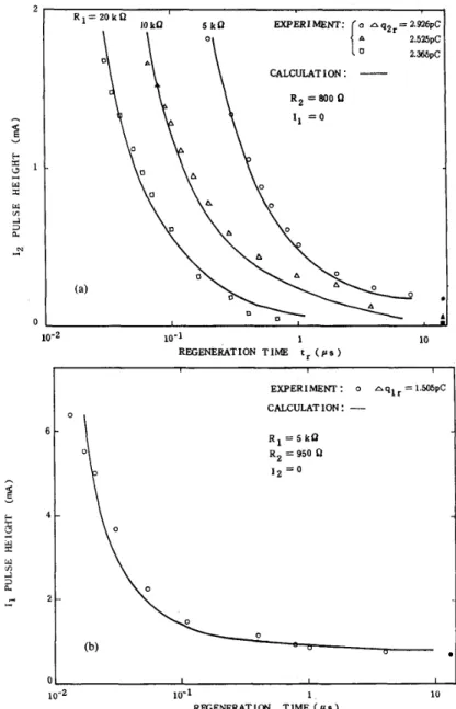
To verify the proposed criterion, the regeneration time t, is calculated by using the above procedure for different pulse heights of I , and I2 and compared to that obtained from SPICE simulations. The results are shown in Fig. 5 where the adopted device parameters are shown in Table I with Aq,,. ( A q 2 , ) found to be 1.49 pC (2.59 pC). As
YANG A N D W U : NEW CRITERION FOR TRANSIENT LATCHUP ANALYSIS U a a 1 - Y - U Q U 0 1341 1 1 PULSE WIDTH=50ns 1 * = 0 I 5 IO 15 20 0 3 c 2 Q
-
n U a Y 3 , Q 1 2 WLSE W I D T H = 5 0 m I , = o 0 5 1 1 5 2 2 5 01’ 0 TIME (ns) (b)Fig. 4. Variation of the charge (a) Aq, and (b) Aq2 with time for different pulse heights of I, or I z applied.
tween theoretical and SPICE simulated results. This sub- stantiates the validity of the dynamic latchup criterion.
It is seen from (20) and (21) that A q , or Aq2 (thus Aql,
or A q 2 , ) are linearly proportional to the average collector junction depletion capacitance ( Tiel
+
cjc2).
Therefore, from the proposed latchup criterion, the regeneration time - t, is also expected to be linearly proportional to ( CjeI+
CJc2).
Fig. 6 shows the variations of calculated and SPICE simulated t, with different zero-biased collector junction depletion capacitances. As can be seen from Fig. 6, the regeneration time indeed increases linearly with the in- crease of the collector junction depletion capacitance, which corresponds to the well-substrate junction deple- tion capacitance. Thus, in contrast to the results of power-up ramp induced latchup [9], larger well-substrate junc- tion depletion capacitance leads to larger regeneration time and higher latchup immunity against pulsed trigger- ing currents.
Fig. 7(a) and (b) shows the variations o f t , with forward transit times of Q , and Q 2 for 5-mA pulse height of I2 and
II , respectively. As the current I2 is applied to the base of Q2, the forward transit time of Q 2 has a stronger effect on t, than that of Q l and t, increases drastically as rF2 increases. However, rFl has a limited effect on the in- crease oft,, as can be seen from Fig. 7(a). The asymmetry in the sensitivity of t, to rFl and 7 F 2 results because the increase of Aq2 ( t ) becomes much slower when 7 ~is in- 2 creased, as compared with that when rF1 is increased.
1342 IEEE TRANSACTIONS O N E L E C T R O N DEVICES, VOL. 36, N O . 1. JULY 1989 S I M U L A T I O N : 0 0 0 C A L C U L A T I O N : - A q Ir = 1.49pC 0 5 10 15 REGENERATION TIME t r (ns) 20
Fig. 5 . Relation between the pulse height of I , or I2 and the regeneration time required for initiating latchup
I I I
S I M U L A T I O N : o o o
CALCULATION -
0 2 4 6 8 10
COLLECTOR JUNCTION CAPACITANCE Cj, ( p f )
Fig. 6. Variation of the regeneration time with collector junction capacitance for 5-mA pulse height of I , or I? applied.
Therefore, increasing the forward transit time T~~ of the lateral p-n-p transistor results in a limited effect on the transient latchup immunity against the well triggering cur- rent. For the current
ZI
applied to the base of Q , , both the increases of 7 ~ 1 and 7 F 2 lead to the increase of t, , but T~~ has a stronger effect on increasing t,, as shown in Fig. 703).The effects of substrate and well resistances on t, are shown in Fig. 8(a) and (b) under
ZI
and Z2 triggerings, respectively. The decrease of R I or R2 leads to an increase oft,.
However, because of the small current gain and large transit time of the lateral p-n-p transistor, which results in a slower increase of Aql with time, the increase of r,. due to the decrease of R2 or R I in the Z2 triggering case is muchYANG A N D W U : NEW CRlTERION FOR TRANSIENT LATCHUP ANALYSIS 5 1343 I I I 0.1 r n = 2 0 n s : - - - rF2 = 0 .Bns :
-
I 2 PULSE HEIGliT=B nu9 I = o I I I I I I I I 1 10 100
FORWARD TfWNSIT TIME ( n s )
(a) '. I r F 1 = 2 0 n s : - - - r F 2 =025ns:
-
l 1 PULSE HEIGHT=5mA I = osmaller than that in the
Zl
triggering case, as can be seen in Fig. 8(a) and (b). This reveals that the efforts of de- creasing the substrate resistance R2 have a limited effect on the transient latchup immunity against the pulsed well triggering current. It should be noted that the decrease of R , or R2 also increases the value of the static well and substrate triggering currents so that latchup immunity is greatly enhanced [6]. However, as long as the pulse height of the triggering current exceeds the static triggering cur- rent, the decrease of R I or R2 becomes more effective inincreasing the regeneration time of
Zl
than that of Z2 in the transient case. Moreover, as shown in Fig. 8, the varia- tion of t , is more sensitive to R 2 ( R 1 ) than to R, ( R 2 ) for the case ofZl
( Z2) triggering current, similar to the results in [lo].The results of Figs. 7 and 8 show that the sensitivity of
r,
to the parameters of Ql and Q 2 depends also on whether the applied pulsed triggering current is a well triggering current or a substrate triggering current. When the well triggering current Z2 is applied to the base node of Q 2 , the1344 IEEE TRANSACTIONS ON ELECTRON DEVICES, VOL. 36. NO. 7, JULY 1989
....
RI =10Kn : - -- R z = I K R : -
12 WLSE HEIGHT = 5mA
l , = O 0 0.1
j
10 100 RESISTANCE (Kn) (a) I I I I R 1 = l O K R :_ _ _ _ _ _
R2 = 1 K R :-
I I I I 1, PULSE H E I G K T = 5 m A I 1 2 = 0\
I I I I I \ 7 1 1 I I 0 . 1 1 1 0 100 R E S I S T A N C E ( K O ) (b)Fig. 8. Dependence of the regeneration time on the substrate and well resistance for 5-mA pulse height of (a) I , and (b) I , applied.
well resistance R I and the parameters of Q 2 have larger effects on t, than the substrate resistance R2 and the pa- rameters of Ql
.
Similarly, rr has a higher sensitivity to the substrate resistance R2 and the parameters of Q , when the substrate triggering currentZI
is applied.V . EXPERIMENT
A p-n-p-n test pattern was designed and fabricated by using the 2-pm p-well technology to investigate the dy- namic triggering characteristics of latchu The surface concentration of the p-well was 1 X 101gcm-3 and the resistivity of the n-substrate was 2-3 Q-cm. The spacing
between n+ and p+ regions in the well was 30, 70, or 170 pm whereas that in the substrate was 40 or 180 pm. The resistance R I or R2 varies with the n + to p+ spacing in the well or substrate. With a 5-V power supply, current pulses with different pulse widths and pulse heights were applied to the n+ region in the substrate or p+ region in the well as the triggering current. At the instant latchup occurred, the pulse width was measured as the regeneration time t ,
.
In the theoretical calculation, the base-emitter voltages VEBl ( t ) and V B E 2 ( t ) are calculated from (1 1) and (12) or from SPICE simulations for each pulse height by using the device parameters in Table 11. The values of Aql and
YANG A N D WU: NEW CRITERION FOR TRANSIENT LATCHUP ANALYSIS Parameter 1345 Q ~ ( P N P )
I
Q ~ ( N P N ) 2 k 1.94 W 236 w v) a 3 0 10-2 10-1 1 10 REGENERATION TIME t r ( p s ) 1 1 I w a a d L-l EXPERIMENT: 0 A q l r = 1 . m P C CALCULATION : - R 1 = 5 k a R2 = 950 Ci 1 2 = oo t
I I I 10-2 10-1 1 10 REGENERATION TIME t r s )Fig. 9. Experimental and calculated results of (a) pulse height of 1, versus regeneration time for different values of R I and (b) pulse height of I , versus regeneration time. The dark circle, triangle, and square represent the corresponding measured static triggering currents.
8,
I
0.0461I
0.048I , ( A )
I
l.lE-16I
1 . 2 6 E - 1 66'
I
4.8E-6I
4.OE-6Aq2 are then calculated from the calculated VEB, ( t ) and
VBE2(t) by using (20) and (21). The regeneration time is thus calculated as the time at which Aql ( A q 2 ) is equal to Fig. 9(a) shows the calculated and experimental results o f t , for various pulse heights of
Z2
with R I as a parameter. The values of the corresponding measured static Z2 trig- gering current from the same structure are also shown in Fig. 9(a) by solid symbols. For the calculated Aq2,
shown in Fig. 9(a), good agreement is obtained between theo- retical and experimental results. As can be seen from Fig. 9(a), t, increases with the decrease of the pulse height ofZ2
and drastically increases with the decrease of R I . More- over, for large values of t,, the value of the pulse height ofZ2
approaches to that of the corresponding static trig-1346 IEEE TRANSACTIONS ON ELECTRON DEVICES, VOL. 36, NO. 7. JULY 1989
gering current as expected. The experimental and calcu- lated results of t,. for various pulse heights of I , and the measured value of I, in the static triggering case are shown in Fig. 9(b), where good agreement is also obtained.
VI. CONCLUSION
The dynamic triggering characteristics of the p-n-p-n structure are described. The junction depletion capaci- tances of parasitic bipolar transistors are found to have significant effects on the transient variations of transistor terminal currents and voltages. Moreover, the charge stored in junction depletion capacitances of a p-n-p-n structure must be larger than some threshold value to maintain the regeneration of the p-n-p-n structure that leads to latchup. This threshold value is found to be in- dependent of the pulse height of the applied triggering currents. The dynamic latchup criterion, therefore, is constructed in terms of the constant charge-storage within the p-n-p-n structure. Both SPICE simulation and exper- imental results show the validity of the proposed crite- rion. It is found that large forward transit times of para- sitic bipolar transistors and large well-substrate junction depletion capacitances lead to the long regeneration time required for sustaining the regeneration of a p-n-p-n struc- ture and thus high latchup immunity against pulsed trig- gering currents.
APPENDIX A
Taking both the high-level injection effect and the sur- face leakage current effect into consideration, the static terminal currents of both transistors can be written as [ 121
APPENDIX B
The collector and emitter junction depletion capaci- tances in (1) to (4) can be written, respectively, as
G e l = q c l O / [ - (VB/BE2
+
VEBI - vDD)/$6]1/3 ( B 1 )G c 2 = G c 2 0 / [ 1 - ( V B E 2 + ‘/BEE, - v D D > / d ) 6 ]
I /3 (B2) for graded junctions and
0 3 3 ) ( B 4 ) 0 5 CJel = G e l O / ( l - V E B l / $ b ) c j e 2 = cje20/(1 - V B E 2 / @ 6 ) 0 5
for abrupt junctions.
- The average junction depletion capacitances
Gel
andGel
can be written from ( B l ) and (B3) asand
where VEBlo and VBno are the corresponding cut-in volt- ages ( = O S 5 V ) of the base-emitter junctions of Q, and Q 2 , respectively.
Ge2
andCje2
have similar expressions.REFERENCES
D. B . Estreich and R. W. Dutton, “Modeling latchup in CMOS in- tegrated circuits,” IEEE Trans. Compurer-Aided Design - of - ICAS, vol. CAD-1, pp. 157-162, 1982.
R. D. Rung and H. Momose, “DC holding and dynamic triggering characteristics of bulk CMOS latchup,” IEEE Trans. Electron De-
vices, vol. ED-30, pp. 1647-1655, 1983.
G. J. Hu, “A better understanding of CMOS latchup,” IEEE Trans.
Electron Devices, vol. ED-31, pp. 62-67, 1984.
J. A. Seitchik, A. Chatterjee, and P. Yang, “An analytic model of holding voltage for latchup in epitaxial CMOS,” IEEE Elecrron De-
vice Lerr., vol. EDL-8, pp. 157-159, 1987.
A. G. Lewis, “Latehup suppression in fine-dimensional shallow p-well CMOS circuits,’’ IEEE Trans. Electron Devices, vol. ED-31, C.-Y. Wu, Y.-H. Wang, C. Chang, and C.-C. Chang, “A new ap- proach to model CMOS latchup,” IEEE Trans. Electron Devices, vol. S . Odanaka, M. Wakabayashi, and T. Ohzone, “The dynamics of latchup turn-on behavior in scaled CMOS,” IEEE Trans. Electron
Devices, vol. ED-32, pp. 1334-1340, 1985.
M. Strzempa-Depre, J. Harter, C. Werner, H. Skapa, and R. Hass- ing, “Static and transient latchup simulation of VLSI-CMOS with an improved physical design model,” IEEE Trans. Electron Devices, R. R. Troutman and H. P. Happe, “A transient analysis of latchup in bulk CMOS,” IEEE Trans. Electron Devices, vol. ED-30, pp. 170- 179, 1983.
G. Goto, H. Takahashi, and T. Nakamura, “Modeling and analysis of transient latchup in double-well bulk CMOS,” IEEE Trans. Elec-
rron Devices, vol. ED-33, pp. 1341-1347, 1987.
pp. 1472-1481, 1984.
ED-32, pp. 1642-1653, 1985.
YANG AND W U : NEW CRITERION FOR TRANSIENT LATCHUP ANALYSIS 1347
[ l l ] W. Li and M. El Nokali, “Transient analysis for a new CMOS latchup model,” Solid-Slate Electron., vol. 30, pp. 1331-1339, 1987. [ 121 I . Getreu, Modeling The Bipolar Transistor. Oregon: Tektronix,
1976.
*
Yeu-Haw Yang was born in Taiwan, Republic of
China, on December 16, 1960. He received the
B . S . degree in electrical engineering from Na- tional Cheng-Kung University, Taiwan, in 1982 and the M S. degree in electrical engineering from National Chiao-Tung University, Hsin-Chu, Tai- wan, in 1984. Currentlv, he is workinn toward the Ph.D. degree at the Institute of Electronics, Na- tional Chiao-Tung University, Hsin-Chu, Tai- wan. His research interests include device tech- nology, CMOS latchup, and timing analysis. During 1987-1988, he was the Research Consultant of United Micro- electronic Corp. (UMC), Hsin-Chu, Taiwan.
Chung-Yu Wu (S’75-M’77) was born i n Chiayi. Taiwan, Republic of China, on May 3 I , 1950 He received the B S degree from the Department of Electrophysics, and the M . S and Ph D degree\ from the Institute of Electronics, National Chiao- Tung University, Hsinchu, Taiwan, Republic of China, in 1972, 1976, and 1980, respectively
During 1975-1976, he studied ferroelectric films on silicon and their device applications During 1976-1979, he engaged in the develop- ment of integrated differential negative resistance devices and their circuit applications, with support from the National Elec- tronics Mass Plan (Semiconductor Devices and Integrated Circuit Tech- nologies) of the National Science Council From 1980 to 1984. he was an Associate Professor at the Institute of Electronics, National Chiao-Tung University During 1984-1986, he was an Associate Professor in the De- partment of Electrical Engineering, Portland State University, Portland, OR Presently he is Professor i n the Department of Electronics Engineering and the Institute of Electronics, National Chiao-Tung University His re- search interests have been in device modeling, integrated-circuit technol- ogies, semiconductor memories, analog integrated circuits, digital inte- grated circuits, and computer-aided circuit design.