New
distributed arithmetic algorithm and its application
to
IDCT
T.-S.Chang, C.Chen and C.-W.Jen
Abstract: Distributed arithmetic @A) has been widely used to implement inner product computations with a fixed input. Conventional ROM-based DA suffers from large ROM requirements. A new DA algorithm is proposed that expands the fxed input instead of the variable input into bit level as in ROM-based DA. Thus the new DA algorithm can take advantage of shared partial sum-of-products and sparse nonzero bits in the fixed input to reduce the number of
computations. Unlike ROM-based DA that stores the precomputed results the new DA algorithm uses a predefined structure to compute results. When applied to a 1-D eight-point DCT system the new DA algorithm only needs 30% of hardware area and has faster speed as compared with ROM- based DA. To illustrate the efficiency of the proposed algorithm a 2-D IDCT chip was implemented using 0 . 8 ~ SPDM CMOS technology. The chip with size 4575 x 5 5 2 5 ~ can deliver a processing rate of 50 Mpixels per second.
1 Introduction
Computation of inner products dominates computation cost in many digital signal processing (DSP) applications. Though inner-product designs using multipliers and accu- mulators (MAC) are fast, the associated cost is intolerable when long-length inner-product computation is considered. Instead of using MAC, distributed arithmetic (DA) [l] uses ROM that stores the precomputed partial sum of inner products. Ths computational efficiency makes DA popular in various DSP applications in which one of the multiplica- tion operands is futed, including filters, convolution and
video processing applications like discrete cosine transfom @CT) and inverse DCT (IDCT) [2, 31.
DCT and IDCT [4] has been selected as an important approach in many video codec standards [5] to reduce the spatial redundancies induced from the correlation of sig- nals. Due to the inherent high computation complexity requirement, high-speed and low-cost designs are inevitable in many real-time video applications. To achieve the goals, most of the VLSI implementations of 2-D DCTflDCT use row-column decomposition to convert a 2-D transform into consecutive 1-D ones and adopt DA to compute I-D DCT/IDCT.
The DA technique distributes arithmetic operations rather than lumps them as multipliers do. Conventional DA [l] called ROM-based DA decomposes the variable input of the inner product into bit level to generate precom- puted data. ROM-based DA uses a ROM table to store the precomputed data, which makes it regular and efficient in silicon area in VLSI implementation. However, when the 0 IEE, 1999
IEE Proceehgs online no. 19990537
DO1 10.lO49/igcds: 19990537
Paper f i t received 11th May 1998 and in revised form 29th March 1999 The authors are with the Department of Electronics Engjneeting National Chiao Tung University, 1001 Ta Hsueh Road, Hsinchu 300, Taiwan, Republic of China
size of the inner product increases the ROM area increases exponentially and becomes impractically large, even using ROM partition [6].
We present a new DA algorithm [7] called adder-based DA for solving the problem. This algorithm, in contrast to conventional DA, decomposes the other operand of inner product into bit level, distributes the multiplication opera- tion, and shares the common summation terms. The adder- based DA exploits the distribution of binary value pattern and may maximise the hardware sharing possibility in the implementation. Therefore the adder-based DA requires
less hardware area and smaller computation cycle time than ROM-based DA. Due to its inherent sharing prop- erty, the proposed adder-based DA technique is very suita- ble for multiple inner-product calculations like DCT and IDCT [7]. Since the adder-based DA shares common sum-
mation terms between computations, it can be regarded as one of the class of the common subexpression algorithms [7-101. Unlike previous word-level sharing algorithms, the bit-level DA formulation provides implementation benefits for efficient bit-serial hardware designs.
2
An inner product of length L is defined as Algorithms and architectures of DA
L
Y
= C A Z X Z (1)2=I
where A , is a fned coefficient, and
X,
is a variable input. To keep equations simple, A , and X , are expressed in unsigned fraction (two’s complement form can also be used) as fol- lows: M A, = A,,,2-j ( 2 )x,
= X z , k 2 - k (3) j = 1 N k = lwhere M is the word length of Ai and N is the word length of
X,.
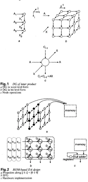
To realise the inner-product computation in eqn. 1 efficiently, using DA is a good strategy from the hardware cost and computing speed points of view. To help the deri- vation and illustrate the difference of different DA approaches, we use both mathematical forms and the dependence gaph (DG) [ll] to represent the two DA approaches. The DG of the two approaches can be derived by proper projection and scheduling of the bit-level DG shown in Fig. 1. A i b 3 f A3 x3 A d4
a b Ci-i C Fig. 1a DG in word level form
b DG in bit level form c Node operations DG of inner product a ... . . . * . . , e , ix :x ' X '
.
. . . .
13; 12; i l j. . . .
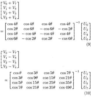
. . . . i%3ix22i%1i I . * . . . . . ... bFig.2 , ROM-hedDA &si@
a Projection along [i k Q = IO 1 01
b SFG
c Hardware implementation
memory
2.1 ROM-based DA
ROM-based DA decomposes the variable input
4
into bit level. Substituting eqn. 3 into eqn. 1 obtainsi=l k l \ k = l
(4) It precomputes these partial products X k I AiX& and stores them in a lookup table ROM for all possible combinations of value. The precomputed values are accessed by the
160
input data and accumulated by shifts. Fig. 2 illustrates the signal flow graph (SFG) of the ROM-based DA design derived by projection along 10 1 01 and the corresponding implementation. Since all nodes along k-planes are
con-
stant, their values can be precomputed and stored in a ROM table. The size of the required ROM tables is pro- portional to 2L. As the length of inner products L becomes
large, the ROM-based DA suffers from extremely large ROM requirements.
2.2 Adder-based DA
Adder-based DA decomposes the fKed coefticients Ai
instead of variable input Xi into bit level. Substituting eqn. 2 into eqn. I obtains
i=l i=l \j=l
A4 / L \
( 5 )
The term ZkIAijX, 3
SJ
is a combination ofX,
since Aij is only 0 or 1. If Xi is a senally input one can obtain Sj bit by bit via serial adders, that isP t=l
Thus eqn. 5 can be rewritten
M M / P \ j=1
P / M \
=
[
c S , , $ 2 - 3)
2-t ( 7 )t=l \;=I 1
Thus, one can shift and then accumulate the term
Sj,r2-J at each cycle t to obtain the inner product. Since
S,
is computed using adders the proposed DA algorithm is called adder-based DA. There are two representations of the adder-based DA for two implementation styles. One isbit-parallel form of eqn. 5 and the other is bit-serial form of eqn. 7. Fig. 3 shows the SFG of the adder-based DA design and the corresponding implementation. All j-planes are combined and collapsed into a summation network, in whch only unique and nonzero nodes have to be com- puted. ... . . . . iA :A j A : , 13; 12: 11; . . . . . . . . . . . . ; b ! A 2 2 ! 4 1 ; . . . . . . . . . . . . iA33j&2i . . . . ... b
Fig. 3 A&-bmed DA &sign
U Projection along k I] = [I 0 01
h SFG
c Hardware implementation
network
Fig. 4 shows an adder-based DA example to illustrate how adder-based DA works. The adder-based DA algo- rithm first decomposes fured coefficients into bit level. After rearranging these terms, one finds that additions are needed only at the nonzero bits of fixed coeficients. This is called zero-one pattern property. In addition, the summation term X I
+
X,
can be shared between bit weights 2l and 2O. This is called common term sharing property. Thus, hard- ware area is saved by exploiting these two properties.input known &fixed * 2'+
Fig. 4 Example ofadder-bmed DA
Fi .5
J a i g o r i l / m A&r-based DA urchitectlae reuhmg bit-seriu/&rm of &r-based
2.3 Architecture design
Fig. 5 shows the adder-based DA architecture realising the bit-serial form of eqn. 5. The architecture consists of an input buffer ('parallel-to-serial converter), a summation net- work, and a shlft-add part. The input buffer converts paral- lel inputs and serially outputs bits of each input. The parallel-to-serial converter can be omitted in the archtec- ture realising the bit-parallel form of eqn. 7. The summa- tion network is a tree structure that connects the required input and generates their summation terms. The summa- tion network of the example is shown in Fig. 6. The shift- add part shifts and accumulates the output of the summa- tion network to generate final inner-product results.
I , I I 1- Fig. 6 2.4 Precision analysis
Given the error constraint, one can derive the required word length of coefficient Ai. If-the coefficient A; has infi- nite precision, Ai has finite word length A4 and \AT - Ad s 2-', the maximum error of the adder-based DA design is
IEE Proc.-Circuits Devices Syst., Vol. 146, No. 4, August 1999
I
L+ L m a x ( X i ) A z 2 - j
j = M + l = L max(Xi) IAi - A,"
1
5
L max(Xi)2-"3 Comparisons with relevant approaches
3. I Comparisons of DA algorithms
To illustrate the area and speed advantages we used 1-D eight-point DCT as an example whose results are shown in Table 1. We only compare ROM tables and summation networks since the two DA methods mainly differ on t h s part. All the data are estimated by using a 0 . 8 ~ SPDM CMOS standard-cell library. The summation network only requires 10Y0 of the transistor counts and 30% of hardware area compared with ROM tables in the ROM-based DA design. The gate area in the summation network is 0.378mm2 that occupies 47.25% of the summation network area. From the Table the adder-based DA design consumes less hardware area and is faster than the ROM-based DA design.
Table 1: Comparisons of ROM and summation network in split kernel eight-point DCT design
Hardware Transistor Estimated Estimated cost count area (include delay time
routing) ROM Eight r6000 2.6mm2 3.6ns 16w x 18b ROM tables Summation 22 serial I 750 0.8mm2 2.4ns network adders
Utilising dflerent function units, the ROM and summa- tion network, results in the different requirements of word length and numbers of accumulation cycle in shift-adders. From eqn. 4, the maximum value of the ROM data in the ROM-based DA design is maxpilAiT,k] = ZslIAiJ. So the output of the ROM should be at least Llog2(E,LI(Ai[)]
+
1 bits wide and the width of the accumulator should also be the same. In the adder-based DA design the accumula- tor is M-bits wide because the summation network gener- ates M-bits output. Hence the adder-based DA design needs shorter word length of shift adders in generating final inner-product results.The number of accumulation cycles in the ROM-based DA design is smaller than that in the adder-based DA design. It needs N accumulation cycles in the ROM-based DA design. However, the accumulators in the adder-based DA design need additional cycles to add the carry from the summation network. The additional number of cycles is
( [log2 maxlCkl
AijTill
+ 1) - N 5 log2 M , which dependson the application specifications. Considering the 2-D IDCT [I31 design example, the input is 12 bits wide and the output will not exceed 12 bits. In this situation no addi- tional cycles are needed.
3.2 Comparison with other subexpression sharing approaches
The proposed DA-based algorithm can be regarded as one of the classes of subexpression sharing techniques whch can be classified according to how the shared common term is generated, as illustrated in Fig. 7. It shows the com- putation of the equation Y = a*xl
+
b*x2+
c*x3+
@x,,where a = OO101Olb, b = 01O101Ob, c = 11101Olb, and d =
11O01Olb. For each sharing type the input to the common term should be available simultaneously for computations. Approaches in [8, 91 generated the shared teims in the word-serial bit-parallel input direction (horizontal circles in Fig. 7). The shared-term generation in [lo] was extended to be in the skewed direction (diagonal circles in Fig. 7). Our proposed approach shared the common terms in the word- parallel bit-serial direction (vertical gray circle in Fig. 7), which is very suitable for the hardware implementation when exploiting the parallel processing features. DA-based approaches can separate the low transition probabihty MSBs from the h g h transition probability LSBs, whch is beneficial to the power management.
Fig. 7 Stuumg tern firnukztwm by dcerent deipressrion sharug approaches
4
For the implementation of the adder-based DA design, eqn. 5 or eqn. 7 can be utilised. Eqn. 5 is suitable for soft- ware implementation while eqn. 7 is suitable for VLSI implementation due to the DA bit-serial nature. Software implementation of eqn. 5 is suitable for simple programma-
ble processor without multipliers since the multiple multi- plication and additions are reduced to just a few operations of shift and addition. Further reduction of operation num- bers can be achieved by combining adder-based DA with fast algorithms. Software implementation of eqn. 5 also
enables adder-based DA to apply to the adaptive designs since we can examine coeficient bits dynamically.
Due to the inherent sharing property, adder-based DA is
very suitable for calculations of multiple inner products. Adder-based DA can share the common computations among multiple inner products and combine them into a summation network. In contrast, the ROM-based DA design has to store-separated ROM tables for each set of
coefficients. The coefficients of multiple inner products can be either multiple dimensional coefficients like DCT or dif- ferent sets of coefficients like DCT and DST. To calculate multiple inner products, just use a summation network to generate the desired subexpressions. If the coeEcient sets are different like DCT and IDCT, use a shuMe network to select the terms required. Fig. 8 shows the architecture for multiple inner product calculations. The drawback of such design is extra shuffle network area and delay.
Issues of adder-based DA design
summation network shuffle network selection Fig. 8 162
Architecture for multiple inner product calculatwns
The optimisation problem of the proposed adder-based design is how to find the common terms from the nonzero subexpressions to reduce the summation network area. Ths is analogous to the logic minimisation problem that extracts the common terms, i.e. a
NP
complete problem. Fortunately, in some real systems like DCT and IDCT, the search space is not large such that one can find the optimal solution by exhaustive search. For more complicated cases, logic minimisation tools can be used to find the solution. Algorithms and optimisation techniques developed in pre- vious subexpression techniques [8-101 can be modified to find efficient common subexpressions by considering the type of adder-based DA subexpressions.In addition to direct optimisation, data partition provides a tradeoff between performance and area as the design specification changes. Data partition can be either data- independent or data-dependent. Data independent method directly partitions vector size L and input word length N , which has been used in previous work on ROM-based DA designs [6]. Data-dependent partition exploits bit patterns of coefficients. The rule for this type of partition is to group the coefficients with similar zero-one patterns into one par- tition. Fig. 9 shows an example on DCT coefficients. Depending on the bit patterns, different realisation meth- ods can achieve lower hardware cost.
~0.11111011~010101
I
,;ze
*1.00000~01p0010101j 0.1 1101 1001000001 1 !
+network ; 0.1 10101001 101 101 1
~0.1011010100000101~
Fig. 9 Exmple ofa'uta-&pe&it parlitition
CSD denotes canonical signed digit coding
5 Application to 2-D IDCT processor
We illustrate a design example of 2-D 8 x 8 IDCT proces-
sor based on proposed adder-based DA approach. This IDCT chip adopts the row-column decomposition to com- pute 2-D IDCT via l-D IDCT. The l-D eight-point IDCT
is first reformulated by the split-kernel method to split the
8 x 8 kernel into two 4 x 4 kernels to reduce computations. The split kernel equations of I-D eight-point IDCT are
vo +
v7 v3+
v4
cos48 cos48 cos48 cos48 cos28 cos60 -cos60 -cos28 cos48 - cos48 -cos48 cos48
cos68 -cos28 cos28 -cos68
(9)
vo
- v7cos8 cos38 cos56 cos78
cos38 cos98 cos158
COS?^^]
[
g]
cos78 cos218 cos358 cos498C O S 5 8 cos158 c0s250 cos35e
(10)
Fig. 10 shows the block diagram of I-D eight-point IDCT. The target throughput rate is one pixel per cycle, that is, the design has to complete 1-D eight-point IDCT computation in eight cycles. To attain such throughput, the
speed of summation networks is designed to do a two-bits addition per cycle since the word length of the input is 12 bits. The common terms of summation networks are searched by the exhaustive method. The IDCT coefficients are first scaled by 42 to reduce the nonzero bits. The scal- ing factor is easily ‘recovered by a shift since row-wise IDCT following by columnwise IDCT willmake the scale factor be two. The serial adder in the summation network is composed of two full adders and a D-fip-flop (DFF)
with reset. The two networks contain 22 full adders, 11 DFFs and 30 output latches. The total gate count of the network is 481, while 40% of the gate count is needed for output latches. The final shift-adders accumulate two 16-bit words per cycle by using a carry save adder and a BLC adder [12].
:I%%; h-h-: ioutwt enable,
I L
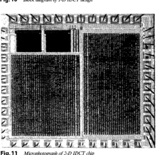
Fig. 11 Microphotograph oj2-D IDCT ch@
Fig. 11 shows the microphotograph of the chip fabri- cated using 0 . 8 ~ SPDM CMOS technology. The chip size is 4575 x 5 5 2 5 ~ and it achieves SOME working fre- quency. The precision of the chip meets the requirement of the IEEE standard [13], as listed in Table 2.
6 Conclusion
We have presented a new DA algorithm called the adder- based DA and its application to 2-D IDCT processor. This algorithm decomposed the fixed coefficients into bit level
Table 2: Precision requirements of IDCT and simulation result
Items Standard Max value
specification of chip
Pixel peak error 1 1
Peak mean square error 0.06 0.0224
Peak mean error 0.015 0.0145
Overall mean square error 0.02 0.0148
Overall mean error 0.0015 0.0012
All zero in all zero out all zero out
instead of decomposing variable input into bit level. Thus, one can exploit the constant and numerical characteristics of the fned input to share and save hardware cost. This effectiveness makes the adder-based DA be a superior design choice over the ROM-based DA in current DA applications. Considering a 1-D DCT design, the adder- based DA only needs 30% of ROM area as compared with the ROM-based DA approach. A 2-D IDCT chp was designed and implemented based on the proposed adder- based DA approach to illustrate the efficiency associated with the proposed approach.
7 Acknowledgment
This work is supported by National Science Council, R.O.C., under the grant NSC-86-2221-E-009-014. 8 References
1 WHITE, S.A.: ‘Applications of distributed arithmetic to digital sequence processing: a tutorial review’, IEEE ASSP Mag., 1989,6, (3), pp. S 1 9
2 SUN, M.T., CHEN, T.C., and GOlTLIEB, A.M.: ‘VLSI implemen- tations of a 16x16 discrete cosine transform’, IEEE Tram. Circuits Svst., 1989. CAS-36, , (4). ~ , I DD.
.-
61M173 URAMOTO,
s.,
INOUE, Y., TAKABATAKE, A., TAKEDA, J., YAMASHITA, H., TERANE, H., and YOSHIMOTO, M.: ‘A 100Mhz 2-D discrete cosine transform core processor’, IEEE J. Solzd- State Circuits, 1992, 21, (4), pp. 492499
4 RAO, K.R. and YIP, P.: ‘Discrete cosine transforms - Algorithms, advantages, applications’ (Academic, Boston, MA, 1990)
5 M O , K.R. and HWANG, J.J.: ‘Techniques and standards for image, video and audio coding’ (Prentice Hall, New Jersey, 1996)
6 NOURJI, K., and DEMASSIEUX, N.: ‘Optimization of real-time VLSI architectures for distributed arithmetic-based algorithms: appli- cation to HDTV filters’. Proceedings of IEEE international sympo- sium on Circuits and systems, 1994, Vol. 4, pp. 223-226
CHEN, C.-S., CHANG, T.-S., and JEN, C.-W.: ‘The IDCT proces- sor on the adder-based distributed arithmetic’. Proceedings of sympo- sium on VLSI circuits, June 1996, pp. 36-37
8 DEMPSTER, A.G., and MACLEOD, M.D.: ‘Use of minimum-adder multiplier blocks in FIR filters’, IEEE Trans. Circuits Syst. II, Analog Digit. Signal Process., 1994,42, (9), pp. 569-577
9 POTKONJAK, M., SRIVASTAVA, M.B., and CHANDRA- KASAN, A.P.: ‘Multiple constant multiplications: eflicient and versa- tile framework and algorithms for exploring common subexpression elimination’, IEEE Trans. Comymt.-Aided Des. Infegr. Circuits Syst.,
10 HARTLEY, R.I.: ‘Subexpression sharing in filters using canonic signed digit multiplier’, IEEE Tram Circuits S-vst. II, Analog Digit. Signal Process., 1996, 43, (lo), pp. 677488
11 KUNG, S.Y.: ‘VLSI array processors’ (Prentice-Hall, New Jersey, 1988)
12 SUZUKI, K., YAMASHINA, M., GOTO, J., INOUE, T., KOSEKI, Y., HORIUCHI, T., HAMATAKE, N., KUMAGAI, K., ENOMOTO, T., and YAMADA, H.: ‘A 2.4 m, 16-bit, 0.5 p,
CMOS arithmetic logic unit for microprogrammable video sequence processor LSIs’. Proceedings of IEEE CICC, May 1993, pp. 12.4.1- 12.4.4
13 IEEE Std 1180-1990: ‘IEEE standard specifications for the implemen- tation of 8x8 inverse discrete cosine transform’
7
1996, 15, (2), pp. 151-165