The resistive switching characteristics in TaON
films for nonvolatile
memory applications
Min-Chen Chen
a, Ting-Chang Chang
a,b,⁎
, Yi-Chieh Chiu
c, Shih-Cheng Chen
d, Sheng-Yao Huang
a,
Kuan-Chang Chang
e, Tsung-Ming Tsai
e, Kai-Hsiang Yang
f, Simon M. Sze
a,c, Ming-Jinn Tsai
ga
Department of Physics, National Sun Yat-Sen University, Kaohsiung 804, Taiwan
b
Advanced Optoelectronics Technology Center, National Cheng Kung University, Taiwan
c
Department of Electronics Engineering, National Chiao Tung University, Hsin-Chu 300, Taiwan
d
Department of Electrical Engineering & Institute of Electronic Engineering, National Tsing Hua University, Hsin-Chu 300, Taiwan
eDepartment of Materials and Optoelectronic Science, National Sun Yat-Sen University, 70 Lien-hai Road, Kaohsiung 804, Taiwan f
Division of Engineering Science, Faculty of Applied Science & Engineering, University of Toronto, Toronto, Ontario, Canada
g
Electronics and Opto-electronics Research Laboratories, Industrial Technology Research Institute, Hsin-Chu 300, Taiwan
a b s t r a c t
a r t i c l e i n f o
Available online 5 November 2012 Keywords:
Resistive switching Nonvolatile memory Tantalum oxynitride (TaON)
In this study, the bipolar resistive switching characteristics of the resistive random access memory (RRAM) device based on sputter-deposited TaON thinfilm were investigated. The proposed memory device exhibits excellent resistance switching behavior with a high resistance state to low resistance state ratio of 2.5 order, write/erase endurance of about 1.5 order, and long retention time of 104s at 85 °C. In addition, the device was investigated to achieve multilevel operation, which could increase storage density for next generation memory application. It was also found that the polarity of the forming process would not influence the resis-tive switching characteristic but would affect thefirst reset process behavior. The switching behavior could be regarded as the oxygen redox near the TiN interface. However, thefirst reset behavior of negative forming process was related to the oxygen concentration gradients near the Pt electrode and the Joule heating en-hanced oxidation.
© 2012 Elsevier B.V. All rights reserved.
1. Introduction
As the demand of powerful mobile electronic products continues to grow, semiconductor nonvolatile memories have been widely applied due to its low power consumption. However, for conventional charge storage-based memories[1–3], the increasing demand for device densi-ties by scaling dimension is expected to be a major challenge due to technical and physical limitations. In order to overcome these problems, new concepts for high density and high-speed nonvolatile memory de-vices have been extensively investigated, including ferroelectric ran-dom access memory (FeRAM)[4], magnetic random access memory (MRAM)[5], phase-change random access memory (PCRAM)[6], and resistive random access memory (RRAM)[7–9]. Among these memo-ries, RRAM has been considered to be the most promising candidate owing to the advantages of its simple structure, low operating power, and fast switching speed. Compared to other current materials, such as perovskite and organic oxides, transition metal oxides have been widely investigated for RRAM devices due to their simple composition and reported outstanding performance[10–15].
In this study, tantalum oxynitride (TaON) fabricated by conventional physical deposition system at room temperature is chosen for RRAM switching layer since the Ta–N thin films, such as Ta2N or TaN, are the
most compatible with the current complementary metal oxide semicon-ductor (CMOS) process[16]. Furthermore, in previous literatures, the TaON interface layer between CuxO and TaN has been regarded as the
main reason for the excellent data retention capability of CuxO RRAM
[17,18].
2. Experimental
A 20 nm-thick TaONfilm was deposited on Si/SiO2/TiN substrates by
RF magnetron sputter deposition using a TaN target in a gas mixture of argon and oxygen (Ar:O2=1:1) at room temperature. The sputtering
power and working pressure werefixed at 100 W and 8 mTorr, respec-tively. Subsequently, 200 nm-thick Pt top electrode was deposited by DC magnetron sputtering system on TaONfilms to form TiN/TaON/Pt struc-ture. Finally, photolithography and lift-off technique were employed to shape the memory cells into a square pattern of 16μm2. Electric
charac-teristics were measured in dark by using an Agilent B1500 semiconduc-tor parameter analyzer. During these measurements, bias was applied to the bottom electrode (TiN) while the top electrode (Pt) was grounded. In addition, X-ray photoelectron spectroscopy (XPS) was used to determine
⁎ Corresponding author at: Department of Physics, National Sun Yat-Sen University, Kaohsiung 804, Taiwan.
E-mail address:[email protected](T.-C. Chang). 0040-6090/$– see front matter © 2012 Elsevier B.V. All rights reserved.
http://dx.doi.org/10.1016/j.tsf.2012.09.081
Contents lists available atSciVerse ScienceDirect
Thin Solid Films
the composition of the TaONfilms. In XPS spectroscopy of as-deposited TaON thinfilms, the binding energies have been corrected by taking the carbon C 1 s peak (285.0 eV) as reference.
3. Results and discussion
Fig. 1(a) shows the XPS spectra in the O 1 s core level region. The en-ergy state at about 530.8 eV is corresponding to TaON[19]. On the other hand, the Ta 4f peak shows an asymmetric shape, which can befitted by four Gaussian distributions, as shown inFig. 1(b). The binding energies of the low-energy-side doublet (Ta 4f7/2=21.8 eV and Ta 4f5/2=23.7 eV)
are in agreement with the values for metallic Ta[19,20]. The energy states at about 25.8 eV and 27.7 eV were corresponding to TaON and TaO bonds, respectively[19,21,22]. According to the analyses and comparison of the peak area of TaON and TaO in Ta 4f XPS spectrum, the chemical composition of TaON layer in this switchingfilm can be indicated as Ta0.3O0.15N0.55. The results revealed that the oxygen reacted with TaN
during the deposition process.
Fig. 2shows the bipolar current–voltage (I–V) characteristics of the TiN/TaON/Pt memory cell in semi-logarithmic scale under DC voltage sweeping mode at room temperature. The initial state of the as-fabricated device is in high resistance state (HRS), and the resistance switching behavior can be obtained repeatedly after a forming process. During the forming process, a positive voltage is applied with a current compliance of 5 mA to prevent device hard breakdown, as shown in the inset ofFig. 2. After the forming process, the memory cell was translated from HRS to low resistance state (LRS). By sweeping the bias from zero to negative over reset voltage of about−0.7 V, the resistance state is transformed from LRS to HRS, called as“reset process”. Conversely, as the voltage sweeps from zero to a positive value, the resistance state turns back to LRS, called as“set process”. During set process, a compli-ance current of 5 mA is applied to prevent permanent breakdown.
To further evaluate the memory performance of TiN/TaON/Pt cell, the endurance test and retention test were measured.Fig. 3(a) shows the endurance characteristics of the device. The resistances are extracted
at afixed voltage of 0.2 V, and the resistance ratio of HRS to LRS is about 101.5times. After 100 switching cycles, it can be seen that the device still
has an acceptable memory window, demonstrating its repetitive switching capability. The retention characteristics of HRS and LRS at T= 85 °C are shown inFig. 3(b). No significant degradation of resistance in HRS and LRS was observed. It indicates that TiN/TaON/Pt device has good reliability for nonvolatile memory applications.
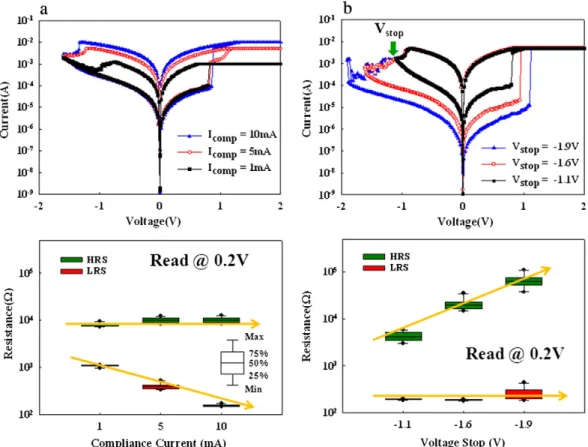
Moreover, multilevel storage technology will be of importance in the development of the next generation memory[23,24]. Hence, the device was investigated to achieve multilevel operation. Fig. 4(a) shows the I–V curves of the device and the statistical charts of the re-sistance in LRS and HRS during 50 switching cycles with different compliance currents. By applying the compliance currents (Icomp) of
1 mA, 5 mA, and 10 mA, three reproducible resistance states can be
Fig. 1. The (a) O 1 s and (b) Ta 4f XPS spectra of as-deposited TaON thinfilms.
Fig. 2. Typical bipolar I–V switching characteristic of the TiN/TaON/Pt memory device with area of 16μm2
in voltage sweeping mode. Inset shows the forming process.
Fig. 3. (a) The endurance performance of the TiN/TaON/Pt cell. (b) Retention behaviors of the HRS and LRS show no degradation at 85 °C. The reading voltage was maintained as 0.2 V.
achieved. The ON-state current increases as Icomp rise while the
OFF-state current seems to not change. The resistance ratio of HRS to LRS ranges from 10 times to 102times as the I
compchange from
1 mA to 10 mA. On the other hand, the multilevel operation can also be performed by controlling the stop voltage (Vstop) at−1.1 V,
−1.6 V, and −1.9 V. Significant changes in OFF-state current during widening the Vstopcan be seen inFig. 4(b). Three states can be
distin-guished clearly. The above results imply that the TiN/TaON/Pt device can be suitable for multilevel application.
In addition, the negative bias forming process was also employed to activate the as-deposited cells, as shown in the inset ofFig. 5. Particular-ly, the polarity of the forming process would not influence the resistive switching behavior. After the negative bias forming, the set process is still achieved under a positive voltage while the reset process is performed under a negative voltage. It should be noted that the reset process was not observed when a positive voltage was applied to the TiN electrode. Besides, the endurance characteristics during continuous 100-times switching cycles are not stable compared to the positive forming device (Fig. 3(a)). According to the above results, Fig. 6(a) shows the schematic diagram of the resistive switching behavior with positive forming process. During the positive forming process, the oxy-gen ions (O2−) are created and drifted toward the TiN electrode, ac-companied by oxygen vacancies (V2+
O) to form the local conductive
paths. Hence, the resistance state is transformed from HRS to LRS. When a negative voltage is applied to the TiN, the movable oxygen ions are repelled from TiN electrode, and recombined with oxygen va-cancies to rupture the conductive paths and induce the reset process. For the negative forming process, as shown inFig 6(b), the movable ox-ygen ions will drift toward the Pt electrode induced by the electrical field. However, the oxygen ion will diffuse away since the inert Pt is un-able to adopt oxygen ions. Applying a negative bias to the TiN after the
negative forming process can present reset behavior by Joule heating due to the higher concentration of oxygen ions near the Pt electrode and cause the rupture offilaments by oxidation close to the Pt electrode
[25]. After that, the mechanism of the resistive switching behavior is the same with the positive forming process, as diagramed inFig. 6(a). In contrast, the reset behavior cannot be observed by applying a positive bias at TiN after the negative forming process. The free oxygen ions will be attracted toward the TiN electrode and absorbed on the TiN elec-trode. Therefore, the conductive paths cannot be ruptured near the Pt electrode due to lack of oxygen ions. On the other hand, thefilament near the TiN electrode cannot be oxidized through Joule heating effect
Fig. 4. The I–V curve of the TiN/TaON/Pt cell and the statistical charts of the resistance in LRS and HRS during 50 switching cycles under (a) different compliance currents and (b) different stop voltages (Vstop).
Fig. 5. The I–V curve of the TiN/TaON/Pt cell with negative forming process. Inset shows the endurance performance of the device.
since the oxygen ions are absorbed on TiN. Therefore, the polarity of the forming process would not influence the resistive switching character-istic but influence the first reset process behavior.
4. Conclusion
In summary, this study investigated the bipolar resistance switching characteristics of the TaON RRAM with the TiN/TaON/Pt structure. The proposed memory device could maintain a HRS/LRS ratio of about 101.5 times during 100 cycle endurance test and the sequential 85 °C retention test for 104s. In addition, multiple levels of resistances can be achieved
using different compliance currents and stop voltages. The resistive switching behavior could be regarded as the formation/rupture of con-ductivefilaments in the TaON layer.
Acknowledgment
This work was performed at National Science Council Core Facilities Laboratory for Nano-Science and Nano-Technology in Kaohsiung-Pingtung area and was supported by the National Science Council of the Republic of China under Contract No. NSC 100-2120-M-110-003.
References
[1] T.C. Chang, F.Y. Jian, S.C. Chen, Y.T. Tsai, Mater. Today 14 (12) (2011) 608. [2] F.M. Yang, T.C. Chang, P.T. Liu, P.H. Yeh, Y.C. Yu, J.Y. Lin, S.M. Sze, J.C. Lou, Appl.
Phys. Lett. 90 (2007) 132102.
[3] F.M. Yang, T.C. Chang, P.T. Liu, U.S. Chen, P.H. Yeh, Y.C. Yu, J.Y. Lin, S.M. Sze, J.C. Lou, Appl. Phys. Lett. 90 (2007) 222104.
[4] N. Setter, D. Damjanovic, L. Eng, G. Fox, S. Gevorgian, S. Hong, A. Kingon, H. Kohlstedt, N.Y. Park, G.B. Stephenson, I. Stolitchnov, A.K. Taganstev, D.V. Taylor, T. Yamada, S. Streiffer, J. Appl. Phys. 100 (2006) 051606.
[5] S. Tehrani, J.M. Slaughter, E. Chen, M. Durlam, J. Shi, M. DeHerrera, IEEE Trans. Magn. 35 (1999) 2814.
[6] S. Lai, IEDM Tech. Dig. (2003) 10.1.1.
[7] Y.E. Syu, T.C. Chang, T.M. Tsai, Y.C. Hung, K.C. Chang, M.J. Tsai, M.J. Kao, S.M. Sze, IEEE Electron Device Lett. 32 (4) (2011) 545.
[8] S. Seo, M.J. Lee, D.H. Seo, E.J. Jeoung, D.-S. Suh, Y.S. Joung, I.K. Yoo, I.R. Hwang, S.H. Kim, I.S. Byun, J.-S. Kim, J.S. Choi, B.H. Park, Appl. Phys. Lett. 85 (2004) 5655. [9] M.J. Lee, S. Han, S.H. Jeon, B.H. Park, B.S. Kang, S.E. Ahn, K.H. Kim, J.H. Lee, Y. Park,
Nano Lett. 9 (2009) 1476.
[10] P.C. Yang, T.C. Chang, S.C. Chen, Y.S. Lin, H.C. Huang, D.S. Gan, Electrochem. Solid State Lett. 14 (2) (2011) H93.
[11] K. Fujiwara, T. Nemoto, M.J. Rozenberg, Y. Nakamura, H.J. Takagi, Jpn. Appl. Phys. 47 (2008) 6266.
[12] M.C. Chen, T.C. Chang, S.Y. Huang, S.C. Chen, C.W. Hu, C.T. Tsai, Simon M. Sze, Electrochem. Solid State Lett. 13 (6) (2010) H191.
[13] M.C. Chen, T.C. Chang, C.T. Tsai, S.Y. Huang, S.C. Chen, C.W. Hu, S.M. Sze, M.J. Tsai, Appl. Phys. Lett. 96 (2010) 262110.
[14] C. Yoshida, K. Kinoshita, T. Yamasaki, Y. Sugiyama, Appl. Phys. Lett. 93 (2008) 042106.
[15] Y.E. Syu, T.C. Chang, C.T. Tsai, G.W. Chang, T.M. Tsai, K.C. Chang, Y.H. Tai, M.J. Tsai, S.M. Sze, Electrochem. Solid State Lett. 14 (10) (2011) H419.
[16] A.E. Kaloyeros, E. Eisenbraun, Annu. Rev. Mater. Sci. 30 (2000) 363.
[17] H.J. Wan, P. Zhou, L. Ye, Y.Y. Lin, J.G. Wu, H. Wu, M.H. Chi, J. Vac. Sci. Technol. B 27 (6) (2009) 2468.
[18] P. Zhou, M. Yin, H.J. Wan, H.B. Lu, T.A. Tang, Y.Y. Lin, Appl. Phys. Lett. 94 (2009) 053510.
[19] W.J. Chun, A. Ishikawa, H. Fujisawa, T. Takata, J.N. Kondo, M. Hara, M. Kawai, Y. Matsumoto, K. Domen, J. Phys. Chem. B 107 (2003) 1798.
[20] J.F. Moulder, W.F. Stickle, P.E. Sobol, K.D. Bomben, Handbook of X-ray Photoelec-tron Spectroscopy, Physical ElecPhotoelec-tronics Inc., Minnesota, 1995.
[21] Q.S. Gao, S.N. Wang, Y.C. Ma, Y. Tang, C. Giordano, M. Antonietti, Angew. Chem. 124 (4) (2012) 985.
[22] K. Kato, H. Toyota, Y. Jin, T. Ono, Vacuum 83 (2008) 592.
[23] S.C. Chen, T.C. Chang, S.Y. Chen, H.W. Li, Y.T. Tsai, C.W. Chen, S.M. Sze, F.S. Yeh(Huang), Y.H. Tai, Electrochem. Solid State Lett. 14 (2) (2011) H103. [24] U. Russo, D. Kamalanathan, D. Ielmini, A.L. Lacaita, M.N. Kozicki, IEEE Trans
Elec-tron Dev. 56 (5) (2009) 1040.
[25] M.C. Chen, T.C. Chang, S.Y. Huang, G.C. Chang, S.C. Chen, H.C. Huang, C.W. Hu, S.M. Sze, T.M. Tsai, D.S. Gan, F.S. Yeh(Huang), M.J. Tsai, Electrochem. Solid State Lett. 14 (12) (2011) H475.