Optoelectronic Properties of Single-Crystalline Zn
2
GeO
4
Nanowires
Chi-Hung Liao,
†Chun-Wei Huang,
†Jui-Yuan Chen,
†Chung-Hua Chiu,
†TzungChuen Tsai,
†Kuo-Chang Lu,
‡Ming-Yen Lu,
§and Wen-Wei Wu*
,††Department of Materials Science and Engineering, National Chiao Tung University, No.1001, University Rd., East Dist., Hsinchu
City 300, Taiwan
‡Department of Materials Science and Engineering, National Cheng Kung University, Tainan 701, Taiwan §Graduate Institute of Opto-Mechatronics, National Chung Cheng University, Chia-yi 621, Taiwan
*
S Supporting InformationABSTRACT: In this work, Zn2GeO4nanowires (NWs) were successfully synthesized on Si(100) substrates through carbon thermal reduction and a vapor−liquid−solid method. The NWs were of around 100 nm diameter and high aspect ratio (AR > 150). High-resolution transmission electron microscopy studies indicate that the NWs are single-crystalline with [110] growth direction. Moreover, the atomic resolution high-angle annular dark-field and bright-dark-field images of scanning transmission electron microscopy have distinguished the different elements. They also further identified the structure of Zn2GeO4 and located the positions of the elements. Additionally, we have fabricated devices and measured the electrical properties of a single NW. It is remarkable that individual Zn2GeO4NW devices exhibited excellent optoelectronic properties with fast switching speed under 254 nm UV illuminations. Furthermore, with short wavelength
UV illumination, as we soaked Zn2GeO4NWs in methyl orange solution, the methyl orange was degraded. Therefore, Zn2GeO4 NWs have potential applications in UV photodetectors and degradation of organic pollutants.
■
INTRODUCTIONRecently, nanoscaled and multifunctional metal oxide nano-structures have attracted extensive attention for potential applications because of their electrical and optoelectrical properties.1−8 As a result, functional 1-D nanostructures of metal oxide nanowires and nanorods have been fabricated by plenty of methods.2 For decades, ternary materials such as Zn2SnO4,9,10Zn2SiO4,11Zn2Ga2O4,12and Zn2GeO413−17 have been of interest because they exhibit physical or chemical advantages by tuning their components. Among these func-tional oxide NWs, the wide-band gap material Zn2GeO4(Eg = 4.68 eV) has promising properties in diverse areas. Also, Zn2GeO4 nanorods were found to be stable photocatalysts in degradation of benzene18and RuO2-dispersed Zn2GeO4showed the potential for decomposing water.19The sheaflike, hyper-branched Zn2GeO4nanostructure displayed photocatalytic properties for reducing CO2 into renewable hydrocarbon fuel.20 Feng et al. proved that Zn2GeO4nanorods could be a candidate as a high-capacity anode for lithium batteries.21Liu et al. reported that native defect phosphor of Zn2GeO4presented white-bluish emission and its photoluminescence was brighter than that of ZnO phosphor,22while Williams et al. reported that Mn2+-doped Zn
2GeO4showed green luminescence.
23
Zn2GeO4has been synthesized by various methods. Tsai et al. fabricated Zn2GeO4 nanostructures by submerging Zn-containing Ge nanoparticles in water at room temperature.13 Yan et al. synthesized nanowires by a chemical vapor transport
method.14 Sun et al. synthesized nanorods by a simple hydrothermal method.24 In this work, we synthesized Zn2GeO4 nanowires by a carbon thermal reduction method. With Au-coatedfilm on Si(100) substrate for catalysis, the high aspect ratio Zn2GeO4 nanowires were synthesized by the vapor−liquid−solid (VLS) mechanism. Furthermore, the atomic resolution annular dark-field (ADF) and annular bright-field (ABF) images of scanning transmission electron microscopy (STEM) were utilized to distinguish the different elements of atoms within the single nanowire. Moreover, we have fabricated devices to measure electrical properties of the single NW. Depositing Au on the nanowires led to a better photocatalytic activity on degrading ethyl range; thus, the effect of Au nanoparticles on degradation has been studied.
■
EXPERIMENTAL SECTIONThe Zn2GeO4 nanowires were synthesized by a three-zone furnace, using the carbon thermal reduction method and vapor−liquid−solid mechanism. The temperature setups of the furnace were 950, 800, and 800°C. The ZnO and Ge powders were prepared with atomic ratio of 2:1 and mixed with 0.23 g of graphite powder in an alumina boat at the upstream zone (950 °C). The 3 nm thick gold film serving as the catalyst was
Received: January 23, 2014 Revised: March 12, 2014 Published: March 21, 2014
deposited on a Si(100) substrate at the midstream zone (800 °C). Carrier gases, argon and oxygen, were adjusted to 50 and 10 sccm, respectively. The temperature was elevated at the rate of 15°C min−1and maintained at specific temperatures for 1 h, while chamber pressure was kept at 3 Torr during the growth of nanowires.
The morphology and crystal structure of Zn2GeO4nanowires were characterized by field emission scanning electron microscope (FESEM, JEOL 6500F) and X-ray diffractometer (XRD, Bruker D2 phaser) using the Cu Kα radiation (λ = 1.54 Å). The crystal structure was further examined by a spherical-aberration corrected field emission transmission electron microscope (Cs-corrected FE TEM, JEOL-ARM200FTH). The electrical and photoresponse properties of a single-wire electric chip exposed to a portable 4 W UV lamp were measured with semiconductor analyzers (Agilent B1500A). The photocatalytic activity for degradation of methyl orange (MO) by Zn2GeO4 NWs was characterized by a Jasco V-670 instrument. The Zn2GeO4 NWs grown on the Si substrate were placed in 20 mL of 5 ppm MO solution under the radiation of a UV lamp (Germicidal Lamps, EYE, G10T8, 10 W). After irradiation for 1 h, the aborption of MO solution was measured by a UV−vis spectrometer. Furthermore, we deposited a 3 nm Au film on the surface of Zn2GeO4 NWs by an e-gun evaporator. After being annealed at 500°C, the Au film transformed to nanoclusters.
■
RESULTS AND DISCUSSIONSynthesis of Zn2GeO4Nanowires. In this study, we used ZnO and Ge powders as experimental sources. The powders were placed upstream at 950°C, evaporated, and transported to midstream by the carrier gases. The melting point of the germanium is 937°C,so the setting temperature would produce germanium vapor. As we mixed ZnO and graphite powders at such a high temperature, zinc vapor was supplied based on previous studies.25 As shown in Figure 1a, high-density Zn2GeO4 NWs were synthesized on the Si(100) substrate under the pressure of 3 Torr. Different synthesis conditions are discussed in Figure S1 of the Supporting Information. Figure 1a shows the high aspect ratio (>150) when the length of grown NWs is greater than 20μm; also, the inset shows the nanowire diameter was about 120 nm. The X-ray diffraction spectrum in Figure 1b corresponds to Zn2GeO4 of a rhombohedral structure (JCPDS card 11-0687) with lattice constants of a = b = 14.231 Å and c = 9.53 Å. The high crystallinity and high aspect ratio of Zn2GeO4 NWs are beneficial for their future applications. In addition, the crystal structure and composition of Zn2GeO4 NWs were analyzed by high-resolution trans-mission electron microscopy (HRTEM) and energy-dispersive spectrometry (EDS). Figure 2a is a low-magnification TEM image of a single Zn2GeO4 nanowire. Figure 2b shows the HRTEM image of the NW, and the inset is its corresponding fast Fourier transform (FFT) diffraction pattern, revealing that the Zn2GeO4nanowire was perfect single-crystalline with [110] growth direction. Figure 2c,d show EDS point and line element analysis. The EDS point analysis indicated that the atomic ratio of Zn and Ge was about 2, which is coherent with the stoichiometry of Zn2GeO4. Also, the line element analysis spectra shows uniform distribution of Zn, Ge, and O.
Panels c and d of Figure 3 are the atomic resolution ADF and ABF images of a Zn2GeO4nanowire along the [001] zone axis, respectively. As we compare Figure 3a,b with the crystal structure illustration, the six-member rings appear explicitly.
The Zn2GeO4belongs to willemite structure (space group 148, R3H). Every Zn and Ge are bonded with four oxygen atoms in tetrahedral structure. Each oxygen is coordinated with one Ge ion and two Zn ions. In conclusion, Zn2GeO4 contains one GeO4 tetrahedron and two ZnO2 tetrahedrals. Because the high-angle annular dark-field and bright-field images were based on the atomic number, we could not identify Zn and Ge because of their similar atomic number. However, remarkably, we observed the atoms with spherical-aberration correctedfield emission transmission electron microscope (Cs correctedfield emission TEM). Because Zn2GeO4is composed of tetrahedral ZnO4 and GeO4, we also analyzed the complex vibration models with FTIR and Raman. The detailed information is represented in Figures S2 and S3 of the Supporting Information.26−28
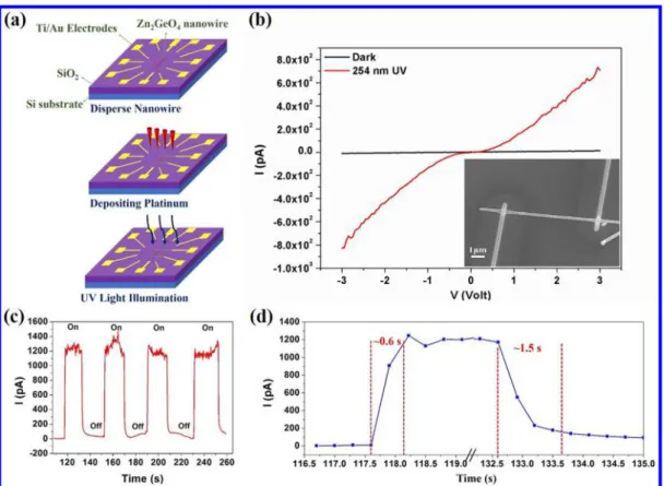
Photodetectors. As illustrated in Figure 4a, we fabricated a single Zn2GeO4nanowire photodetector electrical chip. The Pt electrodes of the device were deposited on the edges of the nanowire by focused ion beam (FIB) which contacted external Au/Ti electrodes. In this study, we compared the current gain in the dark and exposed to 254 nm UV light. The I−V curve in Figure 4b shows that the current in the dark condition was extremely low with a bias of±3 V. Notably, it was exciting that the Zn2GeO4nanowire was sensitive to 254 nm UV light; the Figure 1.(a) FESEM image of Zn2GeO4NWs. The inset is a high-magnification image of the NWs. (b) The XRD pattern shows the high crystallinity of Zn2GeO4.
photocurrent was enhanced at about 800 pA with forward bias of 3 V, which was about 80 times the dark current. While the wide band gap Zn2GeO4was exposed to 254 nm wavelength light, electron−hole pairs were created within the nanowire. We assume the long channel length of the chip from the inset of Figure 4b and high crystallinityof Zn2GeO4NWs as discussed
above, a number of electron−hole pairs would be generated by 254 nm UV light. The response time is defined to be the required interval for increasing 90% of photocurrent variation, while the recovery time is defined to be the decay interval for decreasing 90% of photocurrent variation. The results of photoresponse shown in Figure 4c were conducted at the bias of 3 V. In Figure 4c, we can find alternatively switching behaviors. As for detailed switching time analysis, the response time and recovery time were ∼0.6 and ∼1.5 s, respectively. Schematic illustration of the band structure diagrams and photoconduction mechanism of Zn2GeO4nanowires are shown in Figure 5. Oxygen molecules around the surface of NWs were believed to capture the free electrons within NWs in the dark condition (eq 1), forming the low-conductivity depletion region.1 Plenty of electron−hole pairs could be generated under the illumination of 254 nm UV light (eq 2). Thus, the photocurrent was rapidly generated by the excess moving electrons under the effect of the applied electric field. The generated holes would migrate to the surface, resulting in the recombination of adsorbed negative oxygen ions (O2−) and the decrease of depletion regions. Also, the oxygen molecules could be released to air and residual electrons enhance the photocurrent, which led to optoelectronic properties at the same time (eq 3). After the UV lamp was turned off, the oxygen molecules became negative oxygen ions by charging electrons at the surface as the initial type.
+ −→ − O (g)2 e O (ad)2 (1) → −+ + hv e h (2) + → + − h O (ad)2 O (g)2 (3)
Figure 2.(a) Low-magnification TEM image and (b) HRTEM image of a single Zn2GeO4NW. The inset in (b) is the FFT diffraction pattern corresponding to the [11̅0] zone axis with [110] growth direction. Panels (c) and (d) are the EDS point and line element analysis of the Zn2GeO4 NW, respectively.
Figure 3.(a) Schematic illustration of Zn2GeO4crystal structure along [001] zone axis. (b) Crystal structure with a slight tilt along [001] zone axis and without oxygen atoms. (c,d) Atomic resolution high-angle annular dark-field and bright-field images of a Zn2GeO4 nanowire along [001] zone axis.
According to the above equations and our experimental data, the surface of NWs plays the important role for adsorption and desorption of oxygen molecules. We can attribute the fast switching behaviors to the high aspect ratio of the Zn2GeO4 NWs. Thus, the chip we created with long channel length would acquire the advantage.
Photocatalytic Activity. With the advantage of high aspect ratio of Zn2GeO4NWs, we applied it for degradation of MO. First, we prepared raw Zn2GeO4NWs soaked in MO solution. In Figure 6a, the absorbance at the wavelength of 464 nm
decreased during the increase of reaction time and under the irradiation of 254 nm UV light. Moreover, we fabricated Zn2GeO4 NWs coated with Au nanoparticles. According to previous reports, constructing the heterojunction would decrease the rate of recombination of electron−hole pairs.29,30 As illustrated in Figure 6b and the inset, the Au nanoparticles with diameter of about 10 nm were deposited by e-gun evaporator at the surface of Zn2GeO4 NWs; the EDS spectrum shown in Figure 6c indicated the existence of Au. Moreover, we conducted the blank experiment exposed to 254 nm UV light but without Zn2GeO4NWs. The measurements of degradation of MO are shown in Figure 6d, showing that the UV light had no influence on the pure MO solution. Thus, the reactions for degradation of MO would occur based on the following equations. +hv→e−+h+ Zn GeO2 4 (4) + h+→ · + + H O2 OH H (5) + → · + − h OH OH (6) + · → MO OH degradation of MO (7)
Zn2GeO4NWs obtained sufficient photoenergy to generate electron−hole pairs under irradiation of 254 nm UV light (eq 4). Therefore, the strong oxidation of hydroxyl radicals would happen while H2O reacted with holes (eq 5). Additionally, the hydroxide ions could react with holes to produce hydroxyl radicals. Eventually, the MO solution was degraded by the highly effective hydroxyl radicals (eq 6). With the remarkable photoactivity of Au-coated Zn2GeO4NWs, we propose that the Au nanoparticles would construct a Schottky barrier between Figure 4.(a) Fabricationflow of a single Zn2GeO4nanowire-based electrical chip. (b) I−V curve measured between ±3 V bias in the dark and under exposure to 254 nm UV light. The inset is the SEM image of the photodetector. (c) Switching behaviors for time-dependent photoresponse with 254 nm UV turned on and off repeatedly. (d) Photoresponse and recovery time for a single period of UV light on−off cycle.
Figure 5. Schematic illustration of the mechanism for the photo-detector showing (a) the schematic of the band structure diagrams of a NW in the dark condition and (b) under exposure of 254 nm UV light.
the surface of Zn2GeO4NWs and Au nanoparticles. The shift of Fermi level for decreasing built-in potential resulted from the enhancement of the photocatalytic activity for degradation of MO. The photogenerated electrons would transfer to Au nanoparticles, hindering the recombination of electrons and holes in Zn2GeO4 NWs. Also, the residual holes would continuously react with hydroxide ions and H2O, producing more hydroxyl radicals. Thus, the enhancement of degradation of MO was achieved by the above reactions.
■
CONCLUSIONSIn this study, high-density single crystalline Zn2GeO4 NWs were successfully synthesized on Si(100) substrates by a carbon thermal reduction method. HRTEM images showed the high crystallinity of Zn2GeO4 NWs with [110] growth direction. Furthermore, we have observed the NWs with atomic resolution high-angle annular dark-field and bright-field images of scanning transmission electron microscopy (STEM), on the basis of which we could specify the locations of the atoms. Moreover, the fast switching behaviors demonstrated that the Zn2GeO4NWs of high aspect ratio may serve as building blocks for UV photodetectors. Additionally, the enhancement of the photocatalytic activity for degradation of MO was achieved with Au-coated Zn2GeO4 NWs. For electrons transferred to Au nanoparticles, the recombination of electron−hole pairs was decreased in Zn2GeO4NWs. Thus, the residual holes reacted with H2O and hydroxide ions played the important role in degradation of MO.
■
ASSOCIATED CONTENT*
S Supporting InformationFTIR and Raman spectra of Zn2GeO4 NWs. This material is available free of charge via the Internet at http://pubs.acs.org.
■
AUTHOR INFORMATIONCorresponding Author
*E-mail: [email protected]. Notes
The authors declare no competingfinancial interest.
■
ACKNOWLEDGMENTSThe authors acknowledge the support by National Science Council through Grants 100-2628-E-009-023-MY3, 102-2221-E-009-039, 102-2221-E-006-077-MY3, and 102-2221-E-194-055.
■
REFERENCES(1) Kind, H.; Yan, H. Q.; Messer, B.; Law, M.; Yang, P. D. Nanowire Ultraviolet Photodetectors and Optical Switches. Adv. Mater. 2002, 14, 158−160.
(2) Dai, Z. R.; Pan, Z. W.; Wang, Z. L. Novel Nanostructures of Functional Oxides Synthesized by Thermal Evaporation. Adv. Funct. Mater. 2003, 13, 9−24.
(3) Xu, S.; Qin, Y.; Xu, C.; Wei, Y.; Yang, R.; Wang, Z. L. Self-Powered Nanowire Devices. Nat. Nanotechnol. 2010, 5, 366−373.
(4) Bao, J.; Zimmler, M. A.; Capasso, F.; Wang, X.; Ren, Z. Broadband ZnO Single-Nanowire Light-Emitting Diode. Nano Lett. 2006, 6, 1719−1722.
(5) Chang, S. J.; Hsueh, T. J.; Chen, I. C.; Huang, B. R. Highly Sensitive ZnO Nanowire CO Sensors with the Adsorption of Au Nanoparticles. Nanotechnology 2008, 19, 175502−175506.
(6) Zhou, J.; Gu, Y.; Hu, Y.; Mai, W.; Yeh, P. H.; Bao, G.; Sood, A. K.; Polla, D. L.; Wang, Z. L. Gigantic Enhancement in Response and Reset Time of ZnO UV Nanosensor by Utilizing Schottky Contact and Surface Functionalization. Appl. Phys. Lett. 2009, 94, 191103.
(7) Hsieh, C. Y.; Lu, M. L.; Chen, J. Y.; Chen, Y. T.; Chen, Y. F.; Shih, W. Y.; Shih, W. H. Single ZnO Nanowire−PZT Optothermal Field Effect Transistors. Nanotechnology 2012, 23, 355201−355205. Figure 6.(a) Absorbance spectra for degradation of MO with raw Zn2GeO4NWs during increasing irradiation time. (b) TEM image of Au coated on the surface of Zn2GeO4NWs. The inset is a high-magnification TEM image. (c) EDS pattern of Au-coated Zn2GeO4NWs. (d) Photodegradation of MO under different conditions.
(8) Liang, S.; Sheng, H.; Liu, Y.; Huo, Z.; Lu, Y.; Shen, H. ZnO Schottky Ultraviolet Photodetectors. J. Cryst. Growth. 2001, 225, 110− 113.
(9) Wang, L. S.; Zhang, X. Z.; Liao, X.; Yang, W. G. A Simple Method to Synthesize Single-Crystalline Zn2SnO4(ZTO) Nanowires and Their Photoluminescence Properties. Nanotechnology 2005, 16, 2928−2931.
(10) Jie, J. S.; Wang, G. Z.; Han, X. H.; Fang, J. P.; Yu, Q. X.; Liao, Y.; Xu, B.; Wang, Q. T.; Hou, J. G. Growth of Ternary Oxide Nanowires by Gold-Catalyzed Vapor-Phase Evaporation. J. Phys. Chem. B. 2004, 108, 8249−8253.
(11) Zhou, J.; Liu, J.; Wang, X.; Song, J.; Tummala, R.; Xu, N. S.; Wang, Z. L. Vertically Aligned Zn2SiO4 Nanotube/ZnO Nanowire Heterojunction Arrays. Small 2007, 3, 622−626.
(12) Feng, P.; Zhang, J. Y.; Wan, Q.; Wang, T. H. Photocurrent Characteristics of Individual ZnGa2O4Nanowires. J. Appl. Phys. 2007, 102, 074309.
(13) Tsai, M. Y.; Yu, C. Y.; Wang, C. C.; Perng, T. P. Water-Driven Formation of Luminescent Zn2GeO4Nanorods From Zn-Containing Ge Nanoparticles. Cryst. Growth. Des. 2008, 8, 2264−2269.
(14) Yan, C.; Lee, P. S. Synthesis and Structure Characterization of Ternary Zn2GeO4Nanowires by Chemical Vapor Transport. J. Phys. Chem. C. 2009, 113, 14135−14139.
(15) Bender, J. P.; Wager, J. F.; Kissick, J.; Clark, B. L.; Keszler, D. A. Zn2GeO4:Mn Alternating-Current Thin-Film Electroluminescent Devices. J. Lumin. 2002, 99, 311−324.
(16) Hung, C. C.; Chang, M. P.; Ho, C. Y.; Yu, C. K.; Lin, W. T. Growth of Zn2GeO4and Cu-Doped Zn2GeO4Nanowires by Thermal Evaporation. J. Electrochem. Soc. 2010, 157, 80−83.
(17) Yan, C.; Singh, N.; Lee, P. S. Wide-Band Gap Zn2GeO4 Nanowire Networks as Efficient Ultraviolet Photodetectors with Fast Response and Recovery Time. Appl. Phys. Lett. 2010, 96, 053108.
(18) Huang, J. H.; Wang, X. C.; Hou, Y. D.; Chen, X. F.; Wu, L.; Fu, X. Z. Degradation of Benzene over a Zinc Germinate Photocatalyst under Ambient Conditions. Environ. Sci. Technol. 2008, 42, 7387− 7391.
(19) Sato, J.; Kobayashi, H.; Ikarashi, K.; Saito, N.; Nishiyama, H.; Inoue, Y. Photocatalytic Activity for Water Decomposition of RuO2 -Dispersed Zn2GeO4with d10Configuration. J. Phys. Chem. B. 2004, 108, 4369−4375.
(20) Liu, Q.; Zhou, Y.; Tian, Z. P.; Chen, X. Y.; Gao, J.; Zou, Z. G. Zn2GeO4 Crystal Splitting Toward Sheaf-like, Hyperbranched Nanostructures and Photocatalytic Reduction of CO2 into CH4 under Visible Light after Nitridation. J. Mater. Chem. 2012, 22, 2033−2038.
(21) Feng, J. K.; Lai, M. O.; Lu, L. Zn2GeO4Nanorods Synthesized by Low-Temperature Hydrothermal Growth for High-Capacity Anode of Lithium Battery. Electrochem. Commun. 2011, 13, 287−289.
(22) Liu, Z. S.; Jing, X. P.; Wang, L. X. Luminescence of Native Defects in Zn2GeO4. J. Electrochem. Soc. 2007, 154, H500−H506.
(23) Williams, L. C.; Norton, D.; Budai, J.; Holloway, P. H. Cathodoluminescence from Thin Film Zn2GeO4: Mn Phosphor Grown by Pulsed Laser Deposition. J. Electrochem. Soc. 2004, 151, H188−H191.
(24) Sun, Y.; Yu, L.; Rao, P. Rational Growth of Ternary Zn2GeO4 Nanorods and Self-Assembled Hierarchical Nanostructures. J. Cryst. Growth. 2012, 347, 73−76.
(25) Wang, Z. L. ZnO Nanowire and Nanobelt Platform for Nanotechnology. Mater. Sci. Eng., R 2009, 64, 33−71.
(26) Boppana, V. B. R.; Hould, N. D.; Lobo, R. F. Synthesis, Characterization and Photocatalytic Properties of Novel Zinc Germanate Nano-Materials. J. Solid State Chem. 2011, 184, 1054− 1062.
(27) Xu, J.; Wang, C. R.; Zhang, Y.; Liu, X.; Liu, X. Y.; Huang, S. Y.; Chen, X. S. Structural, Vibrational and Luminescence Properties of Longitudinal Twinning Zn2GeO4 Nanowires. CrystEngComm 2013, 15, 764−768.
(28) Wu, S. P.; Ma, Q. Synthesis, Characterization and Microwave Dielectric Properties of Zn2GeO4Ceramics. J. Alloys Comd. 2013, 567, 40−46.
(29) Subramanian, V.; Wolf, E. E.; Kamat, P. V. Green Emission to Probe Photoinduced Charging Events in ZnO−Au Nanoparticles. Charge Distribution and Fermi-Level Equilibration. J. Phys. Chem. B. 2003, 107, 7479−7485.
(30) Subramanian, V.; Wolf, E. E.; Kamat, P. V. Catalysis with TiO2/ Gold Nanocomposites. Effect of Metal Particle Size on the Fermi Level Equilibration. J. Am. Chem. Soc. 2004, 126, 4943−4950.
![Figure 3. (a) Schematic illustration of Zn 2 GeO 4 crystal structure along [001] zone axis](https://thumb-ap.123doks.com/thumbv2/9libinfo/7717446.146692/3.938.106.426.614.944/figure-schematic-illustration-geo-crystal-structure-zone-axis.webp)