Effects of underlying films on the chemical-mechanical polishing
for shallow trench isolation technology
Y.-L. Wang
a , c ,*, C. Liu
b, M.-S. Feng
b, Jowei Dun
c, K.-S. Chou
c aInstitute of Electronics, National Chiao-Tung University, Hsin-chu, Taiwan b
Institute of Materials Science and Engineering, National Chiao-Tung University, Hsin-chu, Taiwan c
Taiwan Semiconductor Man. Com. Ltd., Fab-4 Eng-2, Science-Based Industrial Park, No. 9, Creation Road 1, Hsin-chu 300, Taiwan
Abstract
The effects of underlying films on the chemical-mechanical polishing (CMP) removal rate have been studied and characterized. A model for the underlying film mechanical properties such as hardness and Young’s modulus, relating to the polishing removal rate was proposed. In addition, a modified shallow trench isolation (STI) process with a thin nitride overcoat has been suggested to eliminate the dishing and oxide remaining on nitride issues. Furthermore, in order to minimize the residual particles and metallic contamination, a modified multi-chemical spray-cleaning process provided for the post-STI CMP cleaning was also studied.1997 Elsevier Science S.A.
Keywords: Chemical-mechanical polishing; Shallow trench isolation technology
1. Introduction
As device geometry continues shrinking, and circuit com-plexity continues growing, device isolation becomes a major factor limiting circuit density. The traditional local oxidation of silicon (LOCOS) has limitations for sub-half-micron generation, due to the lateral encroachment of field oxide upon the device active areas, field oxide thinning in sub-micron regions of exposed silicon, non-planarity, and stress-induced silicon defects [1]. In order to increase device packing density for high performance VLSI/ULSI technol-ogy, shallow trench isolation (STI) becomes attractive because it offers improved isolation between devices com-pared with conventional LOCOS-type isolation techniques. The implementation of STI provides greater packing den-sity, smaller channel-width encroachment, superior latch-up immunity and better planarity [2]. The early trench isolation process uses a plasma etch-back by eroding photoresist and trench oxide simultaneously for planarization [3,4]. How-ever, this complex scheme was not able to provide surface planarity. Recently, chemical-mechanical polishing (CMP) has been intensively studied in planarizing the trench sur-face [5–8]. Although it is well recognized as a powerful
means of global planarization, several issues associated with CMP, including dishing and oxide remaining on nitride, and post-CMP cleaning, have to be addressed before STI replaces LOCOS.
The use of silicon nitride, poly-Si, with thermal or CVD oxide, spin-on-glass (SOG) films to improve the STI process has been reported in the past [4–9]. Since the optimized processing conditions for STI with many kinds of under-lying layers are different than those for CMP of dielectric for back-end-of-line (BEOL), the effect of underlying layers on CMP removal rate needs to be studied in detail. Also, the conventional CMP process contaminates the wafer surface with silica particles and metallic impurities. The silica par-ticles induce defects in VLSI patterns, and metallic impu-rities, even in small quantities, will introduce many crystal defects in Si wafers during furnace processing. Since the planarization of STI is carried out in the front-end-of-line, it is of great importance to remove the residual particles and metallic impurities for improving device yield and perfor-mance. However, since the poly-Si surface is hydrophobic and the SiO2surface is hydrophilic, the Si3N4film charges
easily [9]. Therefore, defects are difficult to remove by con-ventional post-CMP cleaning techniques. Also, the Si sub-strate will be damaged by the conventional scrubber cleaning method if NH4OH chemicals are used only. In
this paper, a new post-CMP cleaning process from the
0040-6090/97/$17.00 1997 Elsevier Science S.A. All rights reserved
P I I S 0 0 4 0 - 6 0 9 0 ( 9 7 ) 0 0 4 9 0 - 2
* Corresponding author. Tel.: +886 3 5781688; fax: +886 3 5790298; e-mail: [email protected]
view point of contamination adhesion mechanism is inves-tigated.
2. Experimental
A Westech Model 472 CMP polisher was used in this study. The wafers used for polishing were 200 mm. Polish-ing was done with commercially available pads designed for global planarization and within wafer uniformity. A fumed silica colloidal suspended in an alkaline medium was rou-tinely used in this study. Five different underlying films were first coated on the blanket test wafers with a thickness of 1000 nm. They were: (1) LPCVD Si3N4(2) LPCVD
poly-Si (3) spin-on-glass (SOG) (4) sputtered aluminum and (5) thermal oxide. These wafers were etched back about 400 nm through the center of the wafer to form a step height across the wafer. A sub-atmospheric chemical vapor deposition (SACVD, 450 Torr) technique was employed to grow 2000 nm O3-TEOS on the wafers. These wafers were then
polished for testing. A SOPRA full spectrum Ellipsometer was used for thickness and removal rate measurement. For pattern wafer experiments, trench regions designed for quarter micron process were patterned and filled by O3
-TEOS for polishing and testing.
In order to develop a post-CMP cleaning method, an OnTrak DSS-200 mechanical scrubber and a multi-chemi-cal spray cleaner, modified from an FSI MERCURY spray processor with different chemical mixtures, such as NH4OH+ H2O2+H2O, HF+H2O and HCl+H2O2 +
H2O have been evaluated. The blanket wafers surface
defects were measured by a Tencor 6420 light-scattering system, and patterned wafer defects were measured by a KLA digital comparison system. The metal contamination was checked by a Rigaju-3700 total reflection of X-ray fluorescence (TXRF) system and secondary ion mass
spec-troscopy (SIMS). Surface roughness was measured by atomic force microscopy (AFM).
3. Results and discussion
3.1. The underlying film’s effect on removal rate
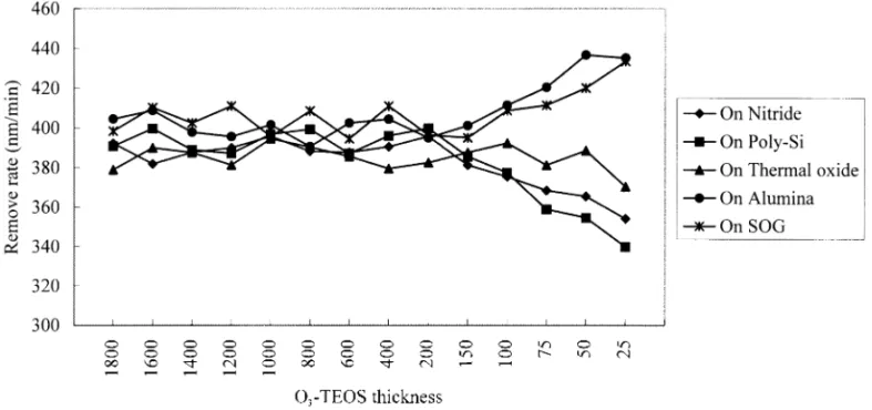
Fig. 1 shows the CMP polishing removal rates of O3
-TEOS for various underlying films versus thickness left of O3-TEOS oxide on the underlying layers, starting from
initial thickness to close to the underlying layers. The curves show that the initial removal rates of O3-TEOS oxide with
these five underlying films are almost the same. The removal rates close to the interface change, and depend on the existing underlying films. It can be seen that the removal rates decrease as the polishing gets close to the underlying layers with poly-Si and nitride films. However, the removal rates increase when the underlying layers are SOG and alu-minum. Scanning electron microscopy (SEM) cross-section pictures were used to check across the edges of underlying layers after polishing. Fig. 2 shows SEM pictures which used poly-Si and SOG as the underlying layers, respec-tively. The results show that a significant step height exists across the edge of the underlying films. In the case of poly-Si as the underlying layer, the O3-TEOS oxide surface is
lower than poly-Si film. In the case of SOG as the under-lying film, the O3-TEOS oxide surface is higher than SOG
film.
In order to characterize the effects of polishing para-meters, such as down force and platen speed, various pol-ishing conditions for the five underlying films were examined. Table 1 shows the results of step height after polishing. They are obtained from SEM directly. It shows that the step height increases with higher down force. No large difference is observed with increasing platen speed.
In order to find out the mechanism of the effects of lying layers, the mechanical properties of these five under-lying films and O3-TEOS oxide were checked. The basic
mechanical properties are presented in Table 2. Both hard-ness and Young’s modulus were measured using the Nano Test 500 Mechanical Properties Microprobe developed by
Micro Materials Ltd. (UK). It can be seen that the higher value of hardness and Young’s modulus of the underlying layers, correlates to a lower interface polishing rate.
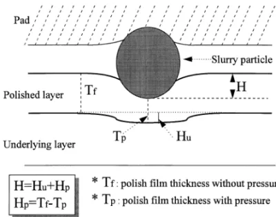
A micro-cutting mechanism is proposed to describe the relation between elastic and plastic deformation and the removal rates of CMP polishing. Fig. 3 displays schemati-cally the mechanical view involved in CMP polishing. As the silica abrasive particles are first driven into the films by the carrier down force, both elastic and plastic deformation occurs. As shown in Fig. 3, the total displacement, H, is a summation of the polished film, Hp, and underlying film Hu,
when the polish front is near underlying film. Thus, the micro-volume on the contact surfaces which will be removed is dependent on the depth pf penetration, H, as shown in Fig. 3. In Eq. (1), the proposed model is that the removal rate (RR ) is a function of H and the polishing distance, L:
R:R:(Removal Rate) =k1×n×d×H×L=t
=k1×n×d× (Hp+Hu) ×n (1)
where k1 is a constant dependent on the chemical and
mechanical effect; d is the cross-sectional area of the abra-sive particle; n is the number of slurry particles which contact the polishing wafer; t is the polishing time and n is the relative velocity between the pad and the surface of Fig. 2. The SEM pictures after CMP polishing for (a) using poly-Si (b)
SOG as underlying layers.
Table 1
The step height (nm) after polishing between O3-TEOS oxide and under-lying films
Underlying layer Polishing conditions
Down force (psi)/ platen rotation speed (rev./min) 6/50 10/50 6/80 Poly-Si −37 −48 −38 Nitride −88 −35 −27 Thermal oxide −10 −14 −10 Aluminum +32 +39 +34 SOG +31 +38 +30
−, O3-TEOS is lower;+, O3-TEOS is higher.
Table 2
The hardness and Young’s moduli for O3-TEOS oxide and underlying films Films Hardness (Gpa) Young’s modulus (Gpa) Poly-Si 89.8 253 Nitride 73.5 201 Thermal oxide 35.9 75 O3-TEOS oxide 27.3 59 SOG 19.8 41 Aluminum 17.4 32
the wafer. The penetration depth is a function of applied pressure p:
H=Hp+Hu
=j=Ep+j=Eu= (1=Ep+1=Eu)j= (1=Ep+1=Eu)k2p (2) where j is the stress and Epand Euare the Young’s moduli
of polishing film and underlying film, respectively. Accord-ing to Eqs. (1) and (2), the removal rate is a function of Young’s modulus, applied pressure, and relative velocity. R:R:=k1×n×d× (1=Ep+1=Eu) ×k2×p×n
=k(1=Ep+1=Eu) ×p×n (3)
where k=k1k2nj. A wear model for the CMP process,
similar in form to Preston’s equation [10] and Cook’s mechanics model, [11] has been developed. With this model, it can be explained that the removal rates with the underlying layers of poly-Si and nitride result in lower values than those of SOG or aluminum. It can be under-stood that the poly-Si and nitride have smaller Huvalues,
consistent with their high hardness and Young’s moduli. A
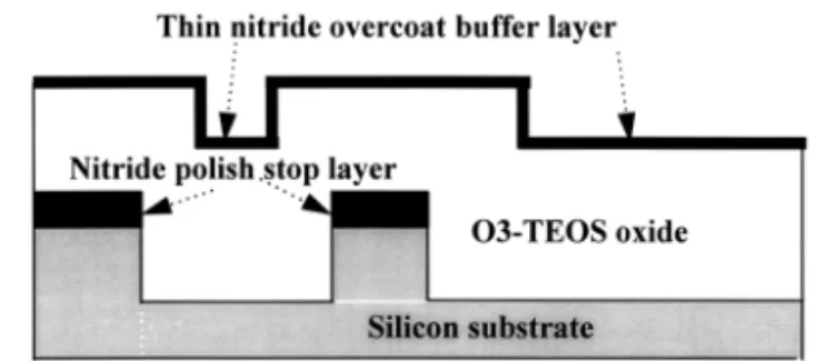
transmission electron microscopy (TEM) picture is pro-vided to prove this model. Fig. 4 shows a TEM picture of aluminum underlying layer cross-section after the wafer is polished. A plastic deformation was observed along the polishing interface. Due to these underlying effects, dishing and oxide remaining on nitride associated with CMP pol-ishing are difficult to prevent. This makes STI difficult because the nitride films are often used as an active region mask layer and CMP polishing stop layer in the conven-tional STI process. In order to reduce these effects, a mod-ified STI process with a thin nitride layer overcoat is proposed. As shown in Fig. 5, a thin 30-nm LPCVD nitride
Fig. 4. The TEM cross-section of the aluminum underlying films after CMP polishing. The plastic deformations were observed along the polished interface. Fig. 5. The modified STI process with a thin nitride overcoat buffer layer.
film was deposited on the O3-TEOS gap filling layer and
the thickness was controlled to maintain uniform step cov-erage. Due to the low polishing removal rate of nitride used as a polishing buffer layer, the problem of dishing and
oxide remaining on nitride was largely reduced. The improved result is shown in Fig. 6. Fig. 6a demonstrates the dishing effect of a conventional STI process and Fig. 6b shows the smooth trench after the modified STI process. 3.2. Post-CMP cleaning for STI
Besides polishing, effective surface cleaning also pre-sents a great challenge for the STI process, because nitride, oxide and poly-Si films may exist simultaneously on wafers after STI polishing. In this paper, a modified multi-chemi-cals spray cleaning for post-STI CMP cleaning was used. The clean sequence and chemicals are listed in Table 3. A modified, heated (75–80°C) ammonia/peroxide mix (APM) clean with 5 s NH4OH (or H2O2) pre-soak time was used first
to pre-wet the polished surface. The NH4OH (or H2O2)
helped to remove slurry particles from the wafer surface. This step changed the sign of the zeta potential between the silica particles and the polished surface. Also, a ramp rin-sing, which was defined as a sequence of high and low turntable rotation speeds such as 500 rev./min → 20 rev./min → 500 rev./min → 60 rev./min helped to phy-Fig. 6. (a) The dishing effect for conventional STI process (b) The smooth
trench after the modified STI process.
Table 3
Clean sequence in post-CMP cleaning for STI Step Cleaning recipe Solution Temperature (°C) Time 1 Pre-soak NH4OH (or H2O2)+H2O 50 10 s 1: 5 2 APM NH4OH+H2O2+H2O 75–80 10 min 1:1:5
3 Ramp rinsing DI water 25 5 min
4 Dilute HF dip HF+H2O 25 10–25 s
1:50
5 Ramp rinsing DI water 25 5 min
6 HPM HCl+H2O2+H2O 75–80 10 min
1:1:6
7 Ramp rinsing DI water 25 5 min
APM, ammonia/peroxide mix; HPM, hydrochloric/peroxide mix.
Table 4
The defect level, metallic contamination (e10 atom/cm2) and surface roughness after post-CMP cleaning for the STI process
Wafers Cleaning Defect
(>0.2 mm) Surface roughness (nm) K Na Fe Cu Ca Blanket O3 -TEOS A 26 0.32 4.72 * 2.04 1.07 3.84 Blanket O3 -TEOS B 29 0.29 26.44 21.78 3.82 0.98 5.92 Blanket nitride A 38 0.47 3.28 * 1.24 0.92 4.37 Blanket nitride0 B 42 0.52 34.33 17.71 5.96 1.88 7.82 Blanket poly-Si A 52 – 9.31 * 2.16 2.98 6.73 Blanket poly-Si B 47 – 23.37 17.58 6.27 3.92 5.25 STI pattern A 68 – – – – – – STI pattern B 72 – – – – – –
sically remove particles. Then the wafers were cleaned by a diluted HF dip. There is a clear purpose in etching a thin layer of hydrous oxide with diluted HF, since the film had been damaged after the CMP process. Finally, metallic ions could be ‘trapped’ in the damaged film and are difficult to remove without a light etching. Consequently, a hydrochlo-ric/peroxide mix (HPM) clean step with high temperature of 75–80°C was used to remove all the metallic ions. This cleaning method enables the formation of soluble com-plexes for improving the solubility. The Cl− anion, in the solution (HPM), is good for complex formation. The metal ion acted as the electron acceptor and the Cl−anion acted as the electron donor in the formation of an inorganic soluble complex. Table 4 shows the effect of the post-CMP cleaning strategy on defect levels, metallic concentration from TXRF, and roughness, from AFM.
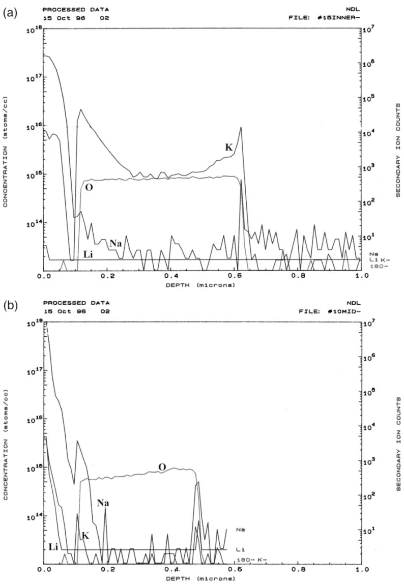
A comparison of this cleaning method with the conven-tional scrubber clean, which is the main choice in most post-CMP applications [12], was also performed. The results are shown in Table 4. In Fig. 7a,b, the SIMS of the oxide wafer for these two clean approaches is shown. In order to elim-inate the surface fluctuation effect of SIMS, the oxide wafers were coated with 100-nm thick poly-Si before ana-lysis. It can be seen that the silica particles and metallic contamination were reduced dramatically for the modified multi-chemicals spray cleaning. Also, in this study, it was found that the clean sequence was important, and different from the conventional RCA clean. If the order of the APM and diluted HF dip steps were switched, particles and metal level would increase by a factor of approximately three or four. The main function of post-CMP cleaning is to remove most of the residue of slurry particles with APM in the first step, and then etch and clean with HF and HCl solution. Without APM cleaning in the first step, residue particles will act as a mask and cannot be etched and cleaned off at the diluted HF dip step. So the APM with NH4OH (or H2O2)
pre-soak time and ramp rinsing step for particle removal play an important role in the post-CMP cleaning process.
4. Conclusion
This work investigates underlying film’s effects on
che-mical-mechanical polishing for STI. Based on underlying films, optimized processing conditions for STI are different from those CMP of dielectric for back-end-of-line (BEOL). It has been shown that the removal rates of CMP for O3
-TEOS oxide on hard films (such as poly-Si and nitride) were smaller than those on soft films (such as SOG and alumi-num). A model related to the underlying film’s mechanical properties was proposed and correlated with experiment results and TEM pictures. A modified STI process with a thin layer of LPCVD nitride overcoat was developed to eliminate the dishing and oxide remaining on nitride issue. A new post-CMP cleaning method for the reduction of metal contamination of different polished film’s surfaces for the STI process was also presented.
References
[1] N. Itoh, C. Yoshino, S. Matsuda, Y. Tsuboi, K. Inou, Y. Katsumata and H. Iwai, IEEE, Bipolar Circuit and Technology Meeting (1992) p. 104.
[2] A. Chatterjee, J. Esquivel, S. Nag, I. Ali, D. Rogers, K. Taylor, K. Joyner, M. Mason, D. Mercer, A. Amerasekera, T. Houston and I.C. Chen, VLSI Technol. 156, (1996).
[3] D.J. Sheldon, C.W. Gruenschlaeger, L. Kammerdiner, N.B. Henis, P. Kelleher and J.D. Hayden, IEEE Trans. Semicond. Manuf. (1988) 140.
[4] P. C. Fazan and V. K. Mathews, IEDM Tech. Dig., 57–60 (1993). [5] B. Davari, C.W. Koburger, R. Schulz, J.D. Warnock, T. Furukawa, M. Jost, Y. Taur, W.G. Schwittek, J.K. DeBrosse, M.L. Kerbaugh and J.L. Mauer, IEDM Technol. Dig., 89–91 (1989).
[6] S.S. Cooperman, A.I. Nasr and G.L. Grula, J. Electrochem. Soc., 142 (1995) 3180.
[7] I. Ali, M. Rodder, S.R. Roy, G. Shinn and M. Islam Raja, J.
Elec-trochem. Soc., 142 (1995) 3088.
[8] L.J. Chen, Y.H. Lee, C.C. Diao, Y.H. Chen, G.G. Lou and J.H. Ho,
Proc. First Internat. Chem.-Mechan. Polish for VLSI/ULSI Multilevel Interconnection Conference, 307 (1996).
[9] N. Miyashita, M. Shimomura, Y. Minami, I. Katakabe, H. Nojo, H. Ohashi and M. Abe, Proc. First Internat. Chem.-Mechan. Polish for
VLSI/ULSI Multilevel Interconnection Conference (CMP-MIC), 161
(1996).
[10] F. Preston, J. Soc. Glass Technol., 11 (1927). [11] L.M. Cook, J. Non-Crystalline Solids, 120 (1990) 152.
[12] W.C. Krusell, J.M. de Larios and J. Zhang, Solid State Technol., (1995) 109