國 立 交 通 大 學
電信工程學系碩士班
碩 士 論 文
IEEE 802.15.3c 多重載波高速介面系統之空間多重擷取
Spatial Division Multiple Access for IEEE 802.15.3c
Multicarrier HSI System
研究生 : 洪郁勛
指導教授 : 吳文榕 博士
IEEE 802.15.3c 多重載波高速介面系統之空間多重擷取
Spatial Division Multiple Access for IEEE 802.15.3c
Multicarrier HSI System
研究生 : 洪郁勛 指導教授 : 吳文榕 教授
國立交通大學電信工程學系碩士班
摘要
IEEE 802.15.3c 為一在短距離傳送未經壓縮的高解析視訊、音訊及資料之規
格。由於使用位於免執照的60GHz 頻帶,因此在此頻帶中將遭受到嚴重的傳播
損耗(propagation loss)。為了解決這項問題,利用平面天線陣列(planar antenna array)及波束形成技術(beamforming)是一個經常使用來補償遺失的方法。在本論 文中,我們首先設計了IEEE802.15.3c 之正交頻分複用技術(OFDM)接收器,並 利用平面天線陣列實現空間分割多重存取(SDMA),進而模擬 IEEE802.15.3c 之 無線個人區域網路(PAN)。在 SDMA 中,各個方向之波束是同時產生的,然而各 個波束之間所形成之干擾成為我們主要關心的問題。最近,一種結合數位權重與 相位偏移器的混合式的天線陣列被提出來。利用這樣的架構之下,可有效的消除 波束之間的干擾。我們利用多重輸入多重輸出(MIMO)系統來模擬 SDMA 系統, 並計算比較SDMA 使用類比波束形成(analog beamforming)與數位波束形成 (digital beamforming)在 IEEE802.15.3c 之下的效能。
Spatial Division Multiple Access for IEEE 802.15.3c
Multicarrier HSI System
Student : Yu-Hsun Hong Advisor : Dr. Wen-Rong Wu
Department of Communication Engineering
National Chiao-Tung University
Abstract
IEEE 802.15.3c is a high data-rate specification proposed to transfer uncompressed high-definition video, audio, and data in short distance. Since it operates in unlicensed 60GHz band, it endures a severe propagation loss. To solve the problem, a planar antenna array conducting beamforming is usually needed to compensate for the loss. In this thesis, we first design an OFDM receiver for the IEEE802.15.3c system. Then, we take advantage of the antenna array to propose a spatial division multiple access (SDMA) system for IEEE802.15.3c personal area network (PAN). In SDMA, multiple beams are formed simultaneously, and interference between these beams becomes the main concern. Recently, a hybrid array, which can conduct beamforming using digital weights and phase shifters, was proposed. With the architecture, interference cancellation becomes possible. We model a SDMA system with a multiple-input-multiple output (MIMO) system and evaluate the performance of an IEEE 802.15.3c SDMA system with analog and hybrid beamforming.
誌謝
首先,我要感謝我的指導教授吳文榕老師在這兩年來的諄諄教誨,引領我在 通訊領域中自由自在的翱翔。老師的治學態度嚴謹,與學生相處卻又如慈父一 般,不論在研究方面,在人生方面,都使我走向了一個全新的境界。我也要感謝 實驗室的李俊芳學長、許兆元學長、曾凡碩學長、謝弘道學長、林鈞陶學長,他 們在課業研究上對我更是不吝指導,猶如一盞明燈點亮了我每個苦思的夜。而碩 士班一同打拚努力的呂珮聰,楊植纓與柯國仁三位同學,不時的關懷與支持,更 是令我深懷感謝之意。另外要感謝伍紹勳教授與行動寬頻無線通訊實驗室的林科 諺同學在研究上給予我的支援。最後,我要感謝我的家人在這兩年來的支持與鼓 勵,我愛你們!Contents
摘要………i Abstract………..ii 誌謝………...iii Contents……….iv List of figures………vi List of tables………...x Chapter 1 Introduction………1Chapter 2 IEEE 802.15.3C Specification Overview………...4
2.1 Introduction………4
2.2 Preamble Structure……….5
2.3 PHY Payload Field……….7
2.3.1 Scrambler………...7
2.3.2 HSI PHY FEC…...……….………...8
2.3.2.1 LDPC Block Code………9
2.3.2.2 Bit Interleaver……….11
2.3.3 Constellation Mapping………12
2.3.4 Spreader………...14
2.3.5 Tone Interleaver………..15
2.3.6 HIS PHY OFDM modulator………...15
2.3.7 Pilot Subcarriers………..16
2.3.8 Guard Subcarriers………17
Chapter 3 IEEE 802.15.3c Receiver Design……….18
3.3 Frequency Synchronization………..20
3.4 Symbol Timing……….22
3.5 Channel Estimation………..23
3.6 Phase Tracking……….…25
Chapter 4 Spatial Division Multiple Access in IEEE 802.15.3c Systems…………28
4.1 Introduction………..28
4.2 Architecture of Planar Antenna Array………..30
4.3 The Array Pattern of Planar Antenna Arrays………30
4.4 MIMO Modeling of SDMA Systems………...36
Chapter 5 MIMO Detectors in OFDM Systems………40
5.1 System Model………...40
5.2 MIMO Detector………42
5.2.1 Zero Forcing and Minimum Mean-Square Error Detectors...42
5.2.2 VBLAST Algorithm………...43
5.2.3 Maximum Likelihood detector………...44
Chapter 6 Simulations………...47
Chapter 7 Conclusions………..……69
7.1 Conclusion………69
7.2 Future work………..70
List of Figure
Figure 2-1 The transmitter block diagram of 802.15.3c HSI PHY………4
Figure 2-2 Realization of scrambling with PRBS generator………..7
Figure 2-3 FEC process for HSI PHY………9
Figure 2-4-1 Parity check matrices of rate-1/2……….10
Figure 2-4-2 Parity check matrices of rate-5/8……….11
Figure 2-4-3 Parity check matrices of rate-3/4……….11
Figure 2-4-4 Parity check matrices of rate-7/8……….11
Figure 2-5 Bit interleaver structure………..12
Figure 2-6 QPSK, 16-QAM, 64-QAM constellation bits encoding……….13
Figure 2-7 Subcarrier frequency allocation………..16
Figure 3-1 Signal flow structure of inner receiver………...18
Figure 3-2 Signal flow structure of the delay and correlate algorithm………19
Figure 3-3 Preamble used for frame detect………..20
Figure 3-4 Preamble used for frequency synchronization………21
Figure 3-5 Preamble used for symbol timing………...23
Figure 3-6 Preamble used for channel estimation………24
Figure 3-7 Signal flow structure of phase compensator………...26
Figure 4-1 Architecture of planar antenna arrays……….29
Figure 4-2 Block diagram of Hybrid Beamforming……….29
Figure 4-3 Configuration of planar antenna arrays………..30
Figure 4-4 Initial structure of planar antenna arrays………33
Figure 4-5 Rearrange structure of planar antenna arrays……….…34
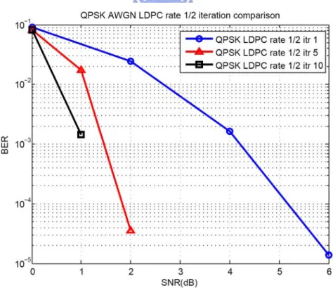
Figure 4-7 Planar antenna arrays of configuration 2 with four weights per user…….35 Figure 4-8 Beamforming pattern with two users (2 weights) between π/2…………..37 Figure 4-9 Beamforming pattern with two users (2 weights) between 3π/4…………37 Figure 4-10 Beamforming pattern with two users (4 weights) between π/2…………38 Figure 4-11 Beamforming pattern with two users (4 weights) between 3π/4………..38 Figure 5-1 MIMO-OFDM transmitter block diagram………..41 Figure 5-2 MIMO-OFDM receiver block diagram………..42 Figure 6-1 BER comparison of LDPC iteration for coding rate 1/2 in QPSK AWGN
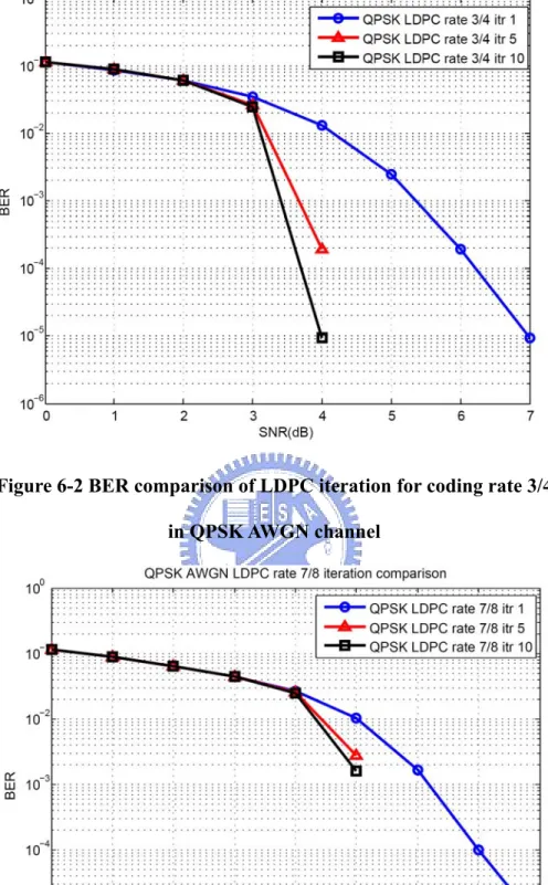
channel………...48 Figure 6-2 BER comparison of LDPC iteration for coding rate 3/4 in QPSK AWGN
channel………...49 Figure 6-3 BER comparison of LDPC iteration for coding rate 7/8 in QPSK AWGN
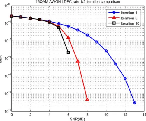
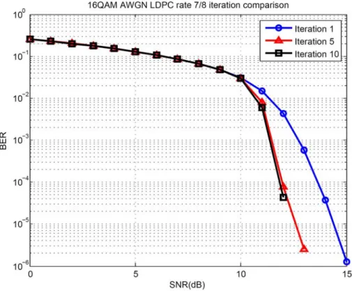
channel………...…49 Figure 6-4 BER comparison of LDPC iteration for coding rate 1/2 in 16QAM AWGN channel………...50 Figure 6-5 BER comparison of LDPC iteration for coding rate 3/4 in 16QAM AWGN channel………...50 Figure 6-6 BER comparison of LDPC iteration for coding rate 7/8 in 16QAM AWGN channel………...……51 Figure 6-7 BER comparison of LDPC iteration for coding rate 5/8 in 64QAM AWGN channel………...………51 Figure 6-8 BER comparison of LDPC iteration for coding rate 1/2 in QPSK multipath Rayleigh fading channel………52 Figure 6-9 BER comparison of LDPC iteration for coding rate 3/4 in QPSK multipath Rayleigh fading channel………52 Figure 6-10 BER comparison of LDPC iteration for coding rate 7/8 in QPSK
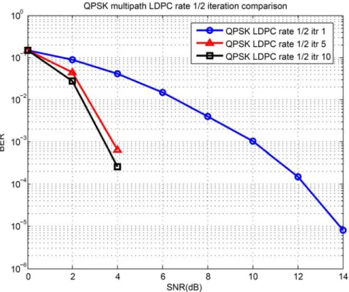
multipath Rayleigh fading channel………..…53
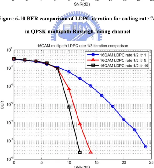
Figure 6-11 BER comparison of LDPC iteration for coding rate 1/2 in 16QAM
multipath Rayleigh fading channel………...…53 Figure 6-12 BER comparison of LDPC iteration for coding rate 3/4 in 16QAM
multipath Rayleigh fading channel………...54 Figure 6-13 BER comparison of LDPC iteration for coding rate 7/8 in 16QAM
multipath Rayleigh fading channel………...54 Figure 6-14 BER comparison of LDPC iteration for coding rate 5/8 in 64QAM
multipath Rayleigh fading channel………...55 Figure 6-15 Comparison of ideal and real-world condition for coding rate 1/2 in
QPSK multipath Rayleigh fading channel………...56
Figure 6-16 Comparison of ideal and real-world condition for coding rate 3/4 in QPSK multipath Rayleigh fading channel………...56 Figure 6-17 Comparison of ideal and real-world condition for coding rate 7/8 in
QPSK multipath Rayleigh fading channel………...57 Figure 6-18 Comparison of ideal and real-world condition for coding rate 1/2 in
16QAM multipath Rayleigh fading channel………....57 Figure 6-19 Comparison of ideal and real-world condition for coding rate 3/4 in
16QAM multipath Rayleigh fading channel………....58 Figure 6-20 Comparison of ideal and real-world condition for coding rate 7/8 in
16QAM multipath Rayleigh fading channel………....58 Figure 6-21 Comparison of ideal and real-world condition for coding rate 5/8 in
64QAM multipath Rayleigh fading channel……….………...59 Figure 6-22 Analog beam pattern I………...…60
Figure 6-24 Hybrid beam pattern I………...60
Figure 6-25 Analog beam pattern II……….61
Figure 6-26 Digital beam pattern II………..…61
Figure 6-27 Hybrid beam pattern II……….…61
Figure 6-28 Performance of SDMA system with analog beamforming using ML detector (IEEE 802.15.3c)………62
Figure 6-29 Performance of SDMA system with analog beamforming using VBLAST MMSE detector (IEEE 802.15.3c)………...…63
Figure 6-30 Performance of SDMA system with analog beamforming using VBLAST ZF detector (IEEE802.15.3c)………...……63
Figure 6-31 Performance of SDMA system with analog beamforming using MMSE detector (IEEE 802.15.3c)………64
Figure 6-32 Performance of SDMA system with analog beamforming using ZF detector (IEEE 802.15.3c)………64
Figure 6-33 Performance of analog beamforming comparison with angle 90°…...…65
Figure 6-34 Performance of analog beamforming comparison with angle 60°….…..66
Figure 6-35 Performance of analog beamforming comparison with angle 15°……...66
Figure 6-36 Performance of analog beamforming comparison with angle 10°….…..67
Figure 6-37 Performance of analog beamforming comparison with angle 5°……….67
Figure 6-38 Performance of SDMA system with hybrid beamforming using ML detector (IEEE 802.15.3c)………69
List if Table
Table 2-1 HSI PHY preamble structure……….5
Table 2-2 Length 128 Golay sequence c128 in hexadecimal notation………6
Table 2-3 Length 128 Golay sequence d128 in hexadecimal notation………6
Table 2-4 LDPC parameters………...9
Table 2-5 Modulation dependent normalization factor………14
Table 2-6 Subcarrier frequency allocation………...16
Table 6-1 HSI PHY MCS dependent parameters……….47
Table 6-2 Power gain with different angles using analog beamforming………..62
Chapter 1 Introduction
With the increasing use of mobile devices in daily life, wireless communication of personal area network (WPAN) becomes more and more important in recent years. Because of the increasing demands for high-quality video applications, IEEE 802.15 WPAN Task Group (TG3c) formed in March 2005 has been developing a millimeter wave alternative physical layer (PHY) for WPAN. The millimeter wave WPAN can operate on the unlicensed band including 57 to 64 GHz. The characteristics of the high penetration loss and strong oxygen adsorption make the radio in 57 to 64 GHz band suitable for short distance transmission. The millimeter wave WPAN also allows coexistence with all other microwave systems defined in the IEEE 802.15 of WPANs. Additionally, it can support high data rate at least 1 Gbps applications such as the high speed internet access or video streaming.
This specification defines two modulation schemes, single-carrier and multicarrier. The multicarrier scheme exploits the orthogonal frequency division multiplexing (OFDM). The OFDM has been shown to be a promising technique and has been used in several wideband digital communication systems, such as the IEEE 802.11 wireless local area network (WLAN), the IEEE 802.16e Worldwide Interoperability for Microwave Access (WiMAX) Wireless MANs and terrestrial digital video broadcasting (DVB-T). The most important advantage of OFDM is that it has the ability to convert the multi-path frequency-selective fading channel into a band of flat fading sub-channels. The receiver can then easily conduct signal recovery with a simple equalization method. Also, OFDM symbols can also be generated by the efficient Fast Fourier transform (FFT) algorithm facilitating its real-world in implementation.
As mentioned, the propagation loss in 60GHz environments is severe. As a result, the antenna array, which can conduct transmit/receive beamforming, is usually equipped in a transceiver. In the IEEE802.15.3c, a PAN is defined in which a user can only communicate with another. With multiple antennas in the transmitter/receiver, however, we can have more advanced applications, e.g, the spatial division multiple access (SDMA). In SDMA, a user can communicate with multiple users simultaneously. In other words, a transmitter/receiver can form multiple beams pointing to multiple directions. As long as the interference between these beams can be controlled under a level, reliable communication between the links can be achieved.
In this thesis, we first design an OFDM receiver for the IEEE802.15.3c system. Then, we propose a SDMA system for IEEE802.15.3c WPAN. For beamforming, a planar antenna arrays with phase shifters for each antenna element is commonly used. Since the phase shift can only adjust the phase of the input signal analog, it cannot conduct interference cancellation. Recently, a hybrid array, which can conduct beamforming using digital weights and phase shifters, was proposed [7]. With the architecture, interference cancellation becomes possible. We will evaluate the performance of an IEEE 802.15.3c SDMA system with analog and hybrid beamforming. Since multiple bit streams are transmitted/received simultaneously in a SDMA system, it can be modeled as a multi-input multi-output (MIMO) system which is also referred to as a multiuser MIMO system. We will use a simple method to provide the modeling.
The rest of this thesis is organized as follow: In Chapter 2, we present the specification of 802.15.3c D04, which include the transmitter structure, preamble structure, and system parameters. In Chapter 3, we design the receiver structure
the hybrid beamforming in [6] and establish the MIMO model for SDMA. In Chapter 5, we describe some commonly used MIMO detection algorithms. In the Chapter 6, we show the simulation result and performance comparison. Finally, we draw conclusions in Chapter 7.
Chapter 2 IEEE 802.15.3C Specification Overview [1]
2.1 Introduction
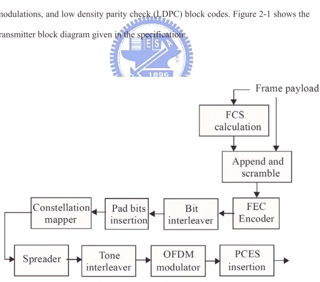
IEEE 802.15.3c is a physical layer specification for high rate wireless personal area networks (WPANs). In this chapter, we will focus on High Speed Interface mode of mmWave PHY (HSI PHY). It is designed for devices with low-latency, bidirectional high-speed data and orthogonal frequency domain multiplexing (OFDM) is used as the modulation scheme. HSI PHY supports a variety of modulation and coding schemes (MCSs) using different frequency-domain spreading factors, modulations, and low density parity check (LDPC) block codes. Figure 2-1 shows the transmitter block diagram given in the specification.
2.2 Preamble structure
A PHY preamble, which is given in Table 2-1, shall be added prior to the frame header to aid receiver operations related to frame detection, auto gain control(AGC) setting, timing acquisition, frequency recovery, frame synchronization, and channel estimation. The PHY preamble shall be transmitted at the rate of RS =5.0625M
samples/s. A preamble symbol is defined as a sequence of length 512 chips which corresponds to the FFT length.
There are defined three different preambles, the mandatory long preamble, mandatory medium preamble, and optional short preamble. All fields of the preambles are based on length 128 complementary Golay sequences c128 and d128, which are given in Table 2-2 and Table 2-3 respectively.
Table 2-2 Length 128 Golay sequence c128 in hexadecimal notation
Table 2-3 Length 128 Golay sequence d128 in hexadecimal notation
Packet synchronization (SYNC) field:
The first field of preamble is used for frame detection, AGC setting, and timing acquisition. The SYNC field in the long preamble is obtained by repeating c128 128 times, and that in the medium and short preamble is obtained by repeating c128 16 times.
Packet start frame delimiter (SFD):
The second field of the preamble, SFD, is provided to establish frame timing, in which length 512 Golay sequences p512 or q512 are used. Sequences p512 or q512 are
constructed from c128 and d128 using the following equations.
512 [ 128 128 128 128]
p = c d c d (2-1)
512 [ 128 128 128 128]
where x denote the complement sequence of x. The long preamble uses the
sequence [p512 p512 p512 p512] whereas the medium preamble uses only [q512] and the short preamble uses [p512] in field SFD.
Channel estimation sequence (CES):
The third field of preamble, which is used to conduct channel estimation, repeats p512 8 times and appends the result to d to construct CES in the long preamble. In 128
medium and short preambles, d is appended to 4 and 2 repetitions of p128 512
respectively.
2.3 PHY pay load field
2.3.1 Scrambler
The frames shall be scrambled by a pseudo-random-bit-stream (PRBS) sequence using a modulo-2 addition, as illustrated below:
Figure 2-2 Realization of scrambling with PRBS generator
15 14 1 ) (D D D g = + + (2-3)
where D is a single bit delay element. The polynomial is a primitive polynomial and it
can generate a maximal length sequence, By the given generator polynomial, the corresponding PRBS, is generated as:
,... 2 , 1 , 0 , 15 14⊕ = =x − x − n xn n n (2-4)
The following sequence defines the initialization sequence:
1 2 3 4 5 6 7 8 9 10 11 12 13 14 15 [ ] init x = x x x x x x x x x x x x x x x− − − − − − − − − − − − − − − [11 01 0 0 0 01 01 1 2 3 4]S S S S = (2-5)
The seed identifier value [S1 S2 S3 S4] is set to 0000, and the first 16 bits will be:
] 0 1 0 1 1 1 0 0 0 1 1 1 1 0 0 0 [ ] ... [x1x2x3 x15 = (2-6)
The scrambled data bits, s , are obtained as follows: n
n n
n b x
s = ⊕ (2-7)
where b represents the unscrambled data bits. The side-stream de-scrambler at the n
receiver shall be initialized with the same initialization vector, x , used in the init
transmitter scrambler.
2.3.2 HSI PHY FEC
Figure 2-3 FEC process for HSI PHY
2.3.2.1 LDPC block code
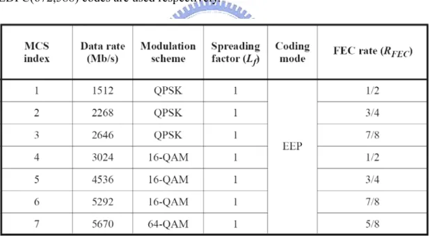
The supported LDPC block FEC rates, information block lengths, LINF, and codeword block lengths, LFEC, are described in Table 2-4
Table 2-4 LDPC parameters
The LDPC encoder is systematic, it encodes an information block of size k, )
,..., ,
(0 1 ( −1) = i i ik
i , into a codeword c of size n, c=(i0,i1,...,i(k−1),p0, p1,...,p(n−k−1)),
by adding n-k parity bits obtained so that HcT =0, where H is an (n – k) × n parity check matrix.
Each of the parity-check matrices can be partitioned into square subblocks (submatrices) of size z × z (z = 21). These submatrices are either cyclic-permutations of the identity matrix or null (all-zero) submatrices. The cyclic-permutation matrix pi is obtained from the z × z identity matrix by cyclically shifting the columns to the right by i elements. An example is showed below, the matrix p0 is the z × z identity matrix, and matrix p1 and p2 are produced by cyclically shifting the columns of the identity matrix I21×21 to the right by 1 and 2 places, respectively.
⎥ ⎥ ⎥ ⎥ ⎥ ⎥ ⎦ ⎤ ⎢ ⎢ ⎢ ⎢ ⎢ ⎢ ⎣ ⎡ = ⎥ ⎥ ⎥ ⎥ ⎥ ⎥ ⎦ ⎤ ⎢ ⎢ ⎢ ⎢ ⎢ ⎢ ⎣ ⎡ = ⎥ ⎥ ⎥ ⎥ ⎥ ⎥ ⎦ ⎤ ⎢ ⎢ ⎢ ⎢ ⎢ ⎢ ⎣ ⎡ = 0 0 1 0 0 0 0 0 0 0 1 1 0 0 0 1 0 0 , 0 1 0 0 0 0 0 0 1 0 0 0 1 1 0 0 , 1 0 0 0 1 0 0 0 0 0 0 1 0 0 0 1 2 1 0 p p p (2-8)
The LDPC encoder supports rate-1/2, rate-5/8, rate-3/4, and rate-7/8 encoding. Figure 2-4 displays the matrix permutation indices of parity-check matrices for all four FEC rates at block length n = 672 bits. The integer i denotes the cyclic-permutation matrix pi. The ‘–’ entries in the table denote null (all zero) submatrices.
Figure 2-4-2 Parity check matrices of rate-5/8
Figure 2-4-3 Parity check matrices of rate-3/4
Figure 2-4-4 Parity check matrices of rate-7/8
2.3.2.2 Bit Interleaver
The bits may be interleaved by a block interleaver which provides robustness against burst errors. The interleaving is performed upon encoded bits with an interleaving depth covering 4 LDPC codewords, over 2688 bits.
The block interleaving process is performed using a permutation ruleL(k). That is, the kth output, written to location k in the output vector, is read from locationL(k)
in the input vector. The block interleaving algorithmL(k)=Ijp,q(k) is described by four parameters: the block size KB =2688, an integer parameter p setting the partition size, an integer parameter q, and the iteration j governing the interleaving spreading. The relationship between the block of KB coded bits, a0, a1, …, aK-1, and
the block of KB interleaved bits, b0, b1, …, bK-1, is given by:
)] ( [ ) (k a I , k b = jpq (2-9)
The interleaving rule for the 1st and the jth iteration is defined as:
(
)
1 , ( ) mod mod , , p q B B B I k = ⎡⎣K − + + ⋅ ⋅p k q p − − ⋅k p k K K ⎤⎦ (2-10)(
1)
, ( ) mod mod , ( ) , , j j p q B p q B B I k = ⎡K − + + ⋅ ⋅p k q p − − ⋅k p I − k K K ⎤ ⎣ ⎦ (2-11)And the binary interleaving parameters shall be: p = 24, q = 2, j = 1. The following figure is an iterative structure of the interleaver.
Figure 2-5 Bit interleaver structure
2.3.3 Constellation Mapping
The coded and interleaved binary serial input data, bi , where i = 0, 1, 2,…, shall
be modulated using QPSK, 16-QAM or 64-QAM modulation. The binary serial stream shall be divided into groups of 2, 4, or 6 bits and converted into complex numbers representing QPSK, 16-QAM or 64-QAM constellation points. The conversion shall be performed according to Gray-coded constellation mappings, illustrated in Figure 2-6 below.
Figure 2-6 QPSK, 16-QAM, 64-QAM constellation bits encoding
The output values, ak, where k = 0, 1, 2,…, are formed by multiplying the
resulting value (Ik + jQk) by a normalization factor KMOD, as ak =(Ik + jQk)×KMOD,
constellation.
Table 2-5 Modulation dependent normalization factor
2.3.4 Spreader
For the spreading factor of 1, the modulated QPSK and QAM complex values ak,
where k = 0, 1, 2, … at the output of the constellation mapper shall be grouped into sets of 336 complex numbers. Each group shall be assigned to an OFDM symbol. This is denoted by the complex number bk,n as
,... 2 , 1 , 0 , 335 ,... 1 , 0 , 336 , =a + × fork = n= bkn k n (2-12)
where n is the OFDM symbol number.
For the spreading factor of 48, the modulated QPSK complex values a(k), where k = 0, 1, 2, … at the output of the constellation mapper shall be grouped into sets of seven complex numbers. This is denoted by the complex number ak,n as
,... 2 , 1 , 0 , 6 : 0 , 28 , =a + × for k= n= akn k n (2-13)
where n is the group number. Each group shall be spread by a factor of 48 to generate a block of 336 complex numbers as follows:
, ( / 28) , * , 335 , , 0 :167 , 168 : 335 k n floor k k n k n k n b q a for k b b − for k = = = = (2-14)
where q is a sequence of length 24 given by:
2.3.5 Tone Interleaver
The tone-interleaver is a bit-reversal tone interleaver which may be combined with the IFFT operation to reduce implementation complexity. The tone interleaver shall be applied to data tones only. Tone interleaver operation is performed by first grouping the complex numbers ak = Ik + jQk at the output of the constellation
mapping into blocks of 336 complex numbers.
2.3.6 HSI PHY OFDM modulator
The discrete-time signal for the nth OFDM symbol is given by
⎥ ⎥ ⎦ ⎤ ⎢ ⎢ ⎣ ⎡ + + =
∑
∑
−∑
= − = × × − = × 1 0 1 0 ) ( 2 , ) ( 2 , 1 0 ) ( 2 , , 1 P G FFT G FFT P D FFT D N m N m N m M k j n m N m M k j n m n N m N m M k j n m FFT n k d e x p e g e N s π π π (2-16)where k∈[0:NFFT −1], ND is the number of data subcarriers, NP is the number of
pilot subcarriers, NR is the number of reserved subcarriers, NG is the number of guard
subcarriers, NFFT is the number of total subcarriers, and dm,n, pm,n, and gm,n, are the
complex numbers placed on the mth data, pilot, and guard subcarriers of the nth OFDM symbol, respectively.
The functions MD(m), MP(m), and MG(m) define a mapping between the indices
[0:ND – 1], [0:NP – 1], [0:NR – 1], and [0:NG – 1] into the logical frequency offset
index [-NFFT / 2 : NFFT / 2 – 1]. The definition for the mapping functions are given
⎩ ⎨ ⎧ ≤ ≤ + ≤ ≤ + − = ⎩ ⎨ ⎧ ≤ ≤ × − + ≤ ≤ × + − = ⎩ ⎨ ⎧ ≤ ≤ + + − ≤ ≤ + − = 15 8 170 7 0 185 ) ( 15 8 ) 22 8 ( 12 7 0 22 166 ) ( 335 168 ] 21 / ) 1 [( 174 167 0 ) 21 / ( 177 ) ( m m m m m M m m m m m M m m round m m m round m m M G P D (2-17)
The mapping of data and pilot subcarriers within an OFDM symbol is illustrated in Figure 2-6. The mapping is further summarized in Table 2-6. As shown in Figure 2-6, there are 16 groups of subcarriers where each group is constituted of 21 data subcarriers and one pilot subcarrier.
Figure 2-7 Subcarrier frequency allocation
Table 2-6 Subcarrier frequency allocation
2.3.7 Pilot subcarriers
suppression. These pilot signals shall be placed into logical frequency subcarriers -166, -144, -122, -100, -78, -56, -34, -12, 12, 34, 56, 78, 100, 122, 144, and 166. The information for the mth pilot subcarrier of the nth OFDM symbol shall be defined as follows: ⎪⎩ ⎪ ⎨ ⎧ = − = + = 14 , 12 , 11 , 10 , 8 , 6 , 4 , 2 , 1 2 / ) 1 ( 15 , 13 , 9 , 7 , 5 , 3 , 0 2 / ) 1 ( m for j m for j pm (2-18) 2.3.8 Guard subcarriers
In all OFDM symbols following the frame preamble, there shall be 16 guard subcarriers, 8 on each edge of the occupied frequency band, at the logical frequency subcarriers -185, -184, …, -178 and 178, 179, …, 185. The data on these subcarriers shall be left to the implementer. Individual implementations may exploit these guard subcarriers for various purposes, including relaxing the specifications on analog transmit and analog receive filters, and possibly peak to average power ratio reduction.
Chapter 3 IEEE 802.15.3c Receiver Design
3.1 Inner receiver structure
An OFDM receiver consists of an inner and outer receiver. The inner receiver conducts synchronization related operations while the outer receiver conducts FEC decoding. The block diagram of the inner receiver is shown in Figure 3-1.
Figure 3-1 Signal flow structure of inner receiver
Detailed operations of the inner receiver conducts include frame detection, timing acquisition, frequency recovery, frame synchronization, and channel estimation. With proper synchronization of the inner receiver, the outer receiver can recover the transmitter data reliably.
3.2 Frame Detection
Frame detection is the task of finding an approximate estimate of the start of the preamble of an incoming data packet. The preamble structure defined in IEEE
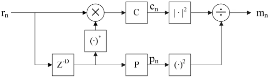
802.15.3c HSI mode enables the receiver to use a simple and efficient algorithm to detect the packet. The algorithm we used is called the delay-and-correlate algorithm, which takes advantage of the periodicity of the SYNC (packet synchronization field) word at the start of the preamble. Figure 3-2 shows the signal flow structure of this algorithm.
Figure 3-2 Signal flow structure of the delay and correlate algorithm
The figure shows two sliding windows C and P. The window C is used to calculate the crosscorrelation between the received signal and a delay version of the received signal. The delay D is equal to the period of the preamble. In the SYNC field, there contains 128 repetitions of a length 128 complementary Golay sequence c128. We choose D=16×128. The window P is used to calculate the received signal energy. The value of the P window is then used to normalize the decision statistic, so that it is independent on the absolute received power level. The decision variable of this algorithm is calculated as 1 * 0 L n n k n k D k c − r r+ + − = =
∑
(3-1) 1 * 0 L n n k D n k D k p − r+ + r+ + = =∑
(3-2) 2 2 ( ) n n n c m p = (3-3)Figure 3-3 Preamble used for frame detect
The decision variable mn is confined between 0 and 1. When the received signal only consists of noise, the output cn of the delayed crosscorrelation is a zero-mean random variable. Once the start of the packet is received, cn is a crosscorrelation of two sets of sixteen c128 symbols. Therefore, mn will jump up quickly to its maximum value, and it can serve as a good indicator of the start of the packet.
3.3 Frequency Synchronization
Both the transmitter and the receiver use their own oscillators to generate carriers and sampling signals. Because of it, the signal generated from the receiver never has the same frequency as it generated from the transmitter. The frequency difference between the transmitter and receiver oscillator is called frequency offset.
One of the main drawbacks of OFDM is its sensitivity to the carrier frequency offset. The carrier frequency offset will reduce the amplitude of subcarriers and cause intercarrier interference (ICI). The preamble allows the receiver to use an efficient maximum likelihood algorithm to estimate and correct for the frequency offset. Let the transmitter signal be s , and the complex baseband model of the passband signal n
n y be 2 tx s j f nT n n y =s e π (3-4) where f is the transmitter carrier frequency, and tx T is the sampling period. After s
complex baseband signal r without the noise term is n 2 2 2 ( ) tx s rx s tx rx s j f nT j f nT n n j f f nT n r s e e s e π π π − − = = 2 s j f nT n s e π Δ = (3-5)
where fΔ = ftx − frx is the difference between the transmitter and receiver carrier frequencies. Let D be the delay between the identical samples of the 12 repeated c128 symbols at the end of SYNC sequence.
Figure 3-4 Preamble used for frequency synchronization
Define an autocorrelation term as 1 * 0 1 2 2 ( ) * 0 1 2 2 ( ) * 0 ( ) ) s s s s L n n D n L j f nT j f n D T n n D n L j f nT j f n D T n n D n z r r s e s e s s e e π π π π Δ Δ Δ Δ − + = − + + = − − + + = = = =
∑
∑
∑
1 2 2 0 s L j f DT n n e π Δ s − = =∑
(3-6) Equation (3-6) is a sum of complex variables with an angle proportional to the frequency offset. Thus, the frequency offset can then be estimated as:1 2 s f z DT π ∧ Δ = − ∠ (3-7)
There is a limitation of the method shown above, i.e., its operating range. The operating range defines how large the frequency offset can be estimated. The range is directly related to the period of the repeated symbols. The angle of z is of the form
s
DT fΔ
−2π , which is unambiguously defined only in the range [−π,π). Thus, if the absolute value of the frequency error is larger than the following limit,
1 2 s 2 S f DT DT π π Δ ≥ = (3-8)
the estimate will be incorrect. This is because z has rotated an angle large than π . For the SYNC sequence, the sample time Ts is 0.39ns, and the delay D is 1536
(12×128). Thus, the maximum frequency error that can be estimated is 834.67 kHz. This should be compared with the maximum allowable frequency error defined in the 802.15.3c system. The maximum tolerance for the transmitted center frequency and chip clock frequency is ±20 ppm. The maximum tolerable frequency error is then 103.68kHz for the chip rate of 2592MHz, which is well within the range of the estimation.
3.4 Symbol Timing
The performance of the symbol timing algorithm directly influences the tolerance of the maximum delay spread of the channel. Specifically, the algorithm is used to locate the starting position of a DFT window. An OFDM receiver achieves its maximum delay spread tolerance when the DFT window starts at the first sample of an OFDM symbol.
As mentioned above, the start edge of a packet can be estimated by the frame detector. This estimate can then be seen as a coarse symbol timing. Since the receiver knows the preamble, it can further use a crosscorrelation based algorithm to refine the
timing. Let tk be a known reference sequence (a portion of the preamble). Then, we can estimate the starting time of the symbol as.
2 1 * 0 arg max L s n n k k k t∧ − r t+ = =
∑
(3-9) where L is the length of the reference sequence. The value of L determines theperformance of the algorithm. A larger value will improve the performance, but also increase the computational complexity. We select two SFD sequences as the reference signal here, which includes two p512 sequences.
Figure 3-5 Preamble used for symbol timing
3.5 Channel Estimation
The channel estimation is the task of estimating the frequency response of the channel that transmitted signal travels before reaching the receiver antenna. We generally assume that the channel is quasi-stationary, which means the channel response does not change during a data packet. Therefore, we only need to estimate the channel once during one packet transmission. We use the CES symbols to estimate the channel response.
The first eight p512 sequences in CES are identical. We can take the advantage of this property to improve the quality of channel estimation. After the DFT, the received CES symbol Rl,k is known to be a product of the CES symbol Xk and the channel Hk
plus additive noise Nl,k, i.e.,
, , 1... , 8
l k k k l k
where n is the number of symbols used for channel estimation.
Figure 3-6 Preamble used for channel estimation Thus the channel response can then be calculated as
1, 2, , 1, 2, , 1, , 1 ˆ ( ) / 1 ( ) / 1 ( ) k k k n k k k k k k k k k k n k k k n k k k k k H R R R X n H X N H X N H X N X n N N H H n X X = + + + = + + + + + = + + + + + 1, , 1 ( ) / k k n k k H N N X n = + + + (3-11)
The noise samples are statistically independent, thus the variance of their n-term average will be reduced to 1/n of the original variance. If n is larger, we can have better estimate with the price of higher computational complexity.
The channel estimation can also be conducted in the time domain. We can calculate the crosscorrelation of the received signal rn and a known reference pk , which is a CES symbol with length L. Theoretically, the resultant signal will give an estimate of the time-domain channel response. To locate the whole response more precisely, we can first find the position of the maximum channel tap which corresponds to the position giving the peak crosscorrelation value, i.e.,
2 1 0 * max arg
∑
− = + = L k k k n n r p peak (3-12)After finding the peak position, we can search backward and forward for 64 taps to locate an area having the maximum energy. We set the number of 64 because the
maximum CP length is 64. Find the average of these 64 taps, set the value to zero which is smaller than average. Then the residual taps are estimated impulse response of channel.
3.6 Phase Tracking
There will always be an error associated with the carrier frequency estimation Thus, there still have some residual frequency error after the frequency offset compensation. The main problem caused by the residual frequency offset is the constellation rotation (phase error), which will influence the demodulation. In this section, we will discuss the phase tracking problem. We first use a data-aided tracking method which exploits the pilot subcarriers to track the phase error. In 802.15.3c, there are 16 pilot subcarriers in the high speed interface mode. With the residual frequency error, the received pilot subcarriers Rn,k will be equal to the product of the
channel frequency response Hk, the known pilot subcarrier Pn,k , and an phase error,
i.e., Δ = j nf k n k k n H P e R 2π , , (3-13) With the estimated channel response Hˆk, we can estimate the phase error as
* , , 1 2 * , , 1 2 2 2 , , 1 ˆ ˆ ( ) ˆ ˆ ( ) (1 ) / 2 p p p N n n k k n k k N j nf k n k k n k k k N j nf k n k n k k R H P H P e H P if H is perfect estimated H P e P i π π Δ Δ = = = ⎡ ⎤ Φ = ∠ ⎢ ⎥ ⎣ ⎦ ⎡ ⎤ = ∠ ⎢ ⎥ ⎣ ⎦ ⎡ ⎤ = ∠⎢ ⎥ = ± ⎣ ⎦
∑
∑
∑
2 2 1 p N j nf k k e π Δ H = ⎡ ⎤ = ∠ ⎢ ⎥ ⎣
∑
⎦ (3-14) To have a more accurate estimation result, we will use a feedback type phase tracking algorithm [2]. The block diagram of the algorithm is shown below.)
(t
Dφ
)
(t
δ
)
(t
Pφ
1 N∑
Figure 3-7 Signal flow structure of phase compensator
The output of the function block “phase estimation” denote as δ(t) that can be obtain by the following procedure
( , ) ( , ) exp( p( )) T t k =R t k ⋅ −jφ t (3-15) 1 ( ) arg( ( ), ( , )) 16k Kp t S k T t k δ ∈ =
∑
(3-16) where Kp denote the index of 16 pilot subcarriers, T(t,k) is a coarse compensated value,and S(k) is the pilot subcarrier data. The final output δ(t) calculate the phase error form T(t,k) and S(k). The pilot subcarrier phase compensation value φp(t) is represented as
(0) 0, ( ) ( 1) ( ), 0 1
p p t p t t
φ = φ =φ − +αδ < <α (3-17) The summation and average block is used for data subcarrier phase compensation
after the phase estimation block. The phase compensation values for data subcarriers and phase compensation with this value are represented as follows
1 1 (0) 0, ( ) ( ) t ( ) D D P i t N t t i N φ φ φ δ = − + = = +
∑
(3-18) ( , ) ( , ) exp( D( 1)) , D D t k =R t k ⋅ −jφ t− k K∈ (3-19) where KD is the set of index of data subcarriers.Chapter 4 Spatial Division Multiple Access in
IEEE802.15.3c Systems
4.1 Introduction
As we know, the IEEE 802.15.3c millimeter-wave alternative physical layer for personal area networks (PAN) can reach high data rate over 1GHz. But it endures some problems such as severe path loss from oxygen absorption and high penetration loss in 60GHz band. To overcome these problems, high gain and high directivity antennas are usually required to compensate for the loss. An effective solution achieving the goals is the use of planar antenna arrays, which can be used to conduct beamforming. An example of an 8 × 8 planar array is shown in Figure 4-1. Note that in the example patch antennas are used. Since the wavelength of the 60GHz signal is short, the antenna array can be fabricated in a small-size silicon. Each of the patch antanna is equipped with a phase shift circuit. By adjusting the phase shift of each antenna, we can steer the beam direction. Note that the phase adjustment is done in the analogy domain. There are two problems with the analog beamforming. The first is that the number of the phases we can adjust may be limited and the phase we adjust may not be accurate. The second is that it can only adjust phase not the amplitude and it cannot conduct interference cancellation.
A more flexible approach is to use the digital beamforming. However, this will require a large amount of digital-to-analogy (D/A) and analog-to-digital (A/D) devices and the implementation cost is greatly enhanced. Recently, a hybrid approach has been proposed [3]-[5], whose block diagram is shown in Figure 4-2. With a limited number of D/A and A/D devices, this approach uses the analogy and digital beamforming simultaneously. In this chapter, we will use the hybrid antenna array to
Note that a local area network has been defined in IEEE 802.15.3c. The use of the SDMA technique can greatly enhance the efficiency of the network.
y x L
φ
θ r w h z dy dxFigure 4-1 Architecture of planar antenna arrays
Dig it al Be am fo rm ing Wei g h t D/A φ1 φk planar antenna planar antenna … …
analog beamforming control
… I Q Mixer Section 1 Input from baseband D/A φ1 φk planar antenna planar antenna … …
analog beamforming control
… I Q Mixer Section N
…
4.2 Architecture of planar antenna arrays
The planar antenna array defined in [6] has 64 identical patch antennas which is form an 8 × 8 antenna matrix. As mentioned, each antenna element has its own phase shifter to manipulate the phase of signal go through it. By beamforming the array to multiple directions, we can conduct the SDMA scheme. There are four D/A and A/D devices in the system. We assume that there are at most two users who a transmitter/receiver can communicate with. The planar antenna array can be partitioned into two kinds of configuration, 1 × 1 and 1 × 2 sections. For configuration 1, all patch antennas are used to support a single user. For configuration 2, the whole 8 × 8 planar antenna array is partitioned into two sections. Each section can serve a user with an 8 × 4 antenna arrays. In configuration 2, the signal of a user will be interfered by the signal from the other user. As a result, we have to conduct interference cancellation.
Figure 4-3 Configuration of planar antenna arrays
4.3 The array pattern of planar antenna arrays [6]
The entire array pattern for a configuration section is computed as the product of the single antenna pattern of the electric field, the analog beamforming pattern and digital beamforming pattern.
( , ) r r r 0
E φ θ =E aθ θ +E aφ φ +E a where E ≅ (4-1)
0 jkr cos cos sin sin
hWkE e Y Z E j X r Y Z θ π φ − ⎡ ⎤ ⎛ ⎞⎛ ⎞ = ⎢ ⎜ ⎟⎜ ⎟⎥ ⎝ ⎠⎝ ⎠ ⎣ ⎦ (4-2)
0 cos sin cos sin sin
jkr hWkE e Y Z E j X r Y Z φ π θ φ − ⎡ ⎛ ⎞⎛ ⎞⎤ = ⎢ ⎜ ⎟⎜ ⎟⎥ ⎝ ⎠⎝ ⎠ ⎣ ⎦ (4-3)
And the corresponding parameters are defined as sin cos 2 kL X θ φ (4-4) sin sin 2 kW Y θ φ (4-5) 2 cos 2 kW Z θ k π λ = (4-6)
where E0 is a constant, W and L are width and length per single antenna element, dx
and dy are the distance in the x and y directions of the adjacent patch antenna, and we
set dx = dy (as shown in Figure 4-1). The parameter k = 2π/dx = 2π/dy .
For a general M × N array, the array pattern of the digital beamforming is defined as [7] ( 1) ( 1) , 1 1 ( , ) x y M N j n j m m n m n DBφ θ w e − ψ e − ψ = = =
∑∑
(4-7) sin cos x kdx ψ θ φ (4-8) sin sin y kdy ψ θ φ (4-9) In this algorithm, we want to steers the main lobe in the direction (φL,θL) and cancels the interference from the direction (φl,θl) where l = 1,…,L-1. Then the algorithm can be rewritten to satisfy the requirement.( 1) ( 1) , 1 1 ( , ) x y M N j n j m m n m n DB φ θ w e − ψ e − ψ = = =
∑∑
( 1)( ) ( 1)( ) 1 1 1 ( x xl )( y yl ) L M N j n j m l l m n b e − ψ ψ− e − ψ ψ− = = = =
∑ ∑
∑
(4-10)And bl can be solved by the following equation
1 1 0 0 1 L L b A b b − ⎛ ⎞ ⎛ ⎞ ⎜ ⎟ ⎜ ⎟ ⎜ ⎟ ⎜ ⎟= ⎜ ⎟ ⎜ ⎟ ⎜ ⎟ ⎜ ⎟ ⎝ ⎠ ⎝ ⎠ (4-11) ( 1)( ) ( 1)( ) , 1 , . 1 1 { } , xk xl yk yl M N j n j m k l k l L k l m n A a ≤ ≤ a e − ψ −ψ e − ψ −ψ = = = =
∑
∑
(4-12)The weight w of digital beamforming pattern can be calculated by m n,
( 1) ( 1) , 1 yl xl L j n j m m n l l w b e− − ψ e− − ψ = =
∑
(4-13) This algorithm is mainly to null the interference introduced by other users.For analog beamforming, the effective weight for an antenna will be ( 1) ( 1) , y x j n j m m n w =e − β e − β (4-14)
where βx and βydenotes the phase shifts along the x-axis and y-axis, respectively. If the main beam in the section has been steered to θd and φd , it can be express as the following equations
sin cos x kdx d d β = − θ φ (4-15) sin sin y kdy d d β = − θ φ (4-16) Using (4-15) and (4-16) in (4-14), we can obtain the antenna pattern for the analogy beamforming. In analogy beamforming, it cannot null the interference from other users, and its performance will be inferior to digital beamforming if interference actually exists.
Now we consider hybrid beamforming with the planar antenna arrays of configuration 1 first. In this case, the overall array pattern is obtained with the
multiplication of the analog and digital beamforming patterns. We first partition the planar antenna arrays into four analog parts, part A, part B, part C and part D.
Figure 4-4 Initial structure of planar antenna arrays
Each of them has its own weight to form the digital beamforming pattern. According to this configuration, we can the antenna pattern as
4 sin sin 4 sin sin
4 sin cos 4 sin cos
1 2 3 4
( , ) jk dx jk dy jk dx jk dy
DBφ θ =w +w e θ φ +w e θ φ +w e θ φe θ φ (4-17)
where wn for n = 1, 2, 3, 4 is corresponding to digital weight, and 4dx and 4dy denote
the distance in the x and y directions of the adjacent analog parts. And the analog beamforming pattern of each part can be written multiplying two linear array factors along x-axis and y-axis, and present as
3 3 ( ) ( ) 0 0 ( , ) jm x x jn y y m n RF
φ θ
e ψ +β e ψ +β = = =∑∑
(4-18) xBut in this partition method, the antenna pattern has many four times of more sidelobes. Therefore, it cannot have the best performance. To solve this problem, we can rearrange the planar antenna arrays in some special way. In the previous method, we directly separate planar antenna arrays into four parts and every part has 16 antenna elements. Now we take one antenna element of each analog part to form a small group repeatedly, and then will have 16 small groups. Use these 16 groups to reconstruct the 8 × 8 planar antenna arrays as figure 4-4 shows. The analog and digital beamforming pattern can be rewritten as
3 3 2 ( ) 2 ( ) 0 0 ( , ) j m x x j n y y m n RF
φ θ
e ψ +β e ψ +β = = =∑∑
(4-19)sin sin sin sin
sin cos sin cos
1 2 3 4
( , ) jkdx jkdy jkdx jkdy
DBφ θ =w +w e θ φ +w e θ φ +w e θ φe θ φ (4-20)
Figure 4-5 Rearrange structure of planar antenna arrays
In the view of digital beamforming pattern, distance between different different parts reduces to dx and dy . For analog beamforming pattern, distance between adjacent
Next we consider about the planar antenna array of configuration 2. In configuration 2, we use two weights or four weights to form the digital beamforming for each user. The antenna array will be reconstructed as follow
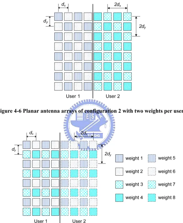
Figure 4-6 Planar antenna arrays of configuration 2 with two weights per user
Figure 4-7 Planar antenna arrays of configuration 2 with four weights per user The analog and digital beamforming pattern for user 1 for the case where two weights are used for each user can be represent as
1 3 2 ( ) 2 ( ) 0 0 ( , ) j m x x j n y y m n RF
φ θ
e ψ +β e ψ +β = = =∑∑
(4-21)sin sin sin sin
sin cos sin cos
1 2
( , ) (1 jkdx jkdy ) ( jkdx jkdy )
DB φ θ =w +e θ φe θ φ +w e θ φ +e θ φ (4-22)
and for the case where four weights are used for each user can be represented as
1 3 2 ( ) 2 ( ) 0 0 ( , ) j m x x j n y y m n RF
φ θ
e ψ +β e ψ +β = = =∑∑
(4-23)sin sin sin sin
sin cos sin cos
1 2 3 4
( , ) jkdx jkdy jkdx jkdy
DBφ θ =w +w e θ φ +w e θ φ +w e θ φe θ φ (4-24)
The quality of the received signal of a user can be seriously affected by the multiple access interference in the SDMA system in the analogy beamforming system. By using the hybrid beamforming, the main beam of user 1 can be adjusted towards the direction of the null array factors of user 2, and vice versa. In this way, we can achieve higher SINR at the desired direction.
4.4 MIMO modeling of SDMA systems
We want to model the SDMA system with the planar antenna arrays as a MIMO system. For a two-user beamforming system, we have from two beams pointing to two desired directions. When considering one user, the signal for the other user will be viewed as interference. Two examples of the beamforming pattern with two users are shown below.
Figure 4-8 Beamforming pattern with two users (2 weights) between π/2
In this figure, we set θ as π/4 and φ for user 1 is π/4 for user 2 is -π/4. Note that two weights are used per user.
Figure 4-9 Beamforming pattern with two users (2 weights) between 3π/4
In this figure, we set θ as π/4 and φ for user 1 is π/8 for user 2 is 7π/8. Note that two weights are used per user.
Figure 4-10 Beamforming pattern with two users (4 weights) between π/2 In this figure, we set θ as π/4 and φ for user 1 is π/4 for user 2 is -π/4. Note that four weights are used per user.
Figure 4-11 Beamforming pattern with two users (4 weights) between 3π/4
In this figure, we set θ as π/4 and φ for user 1 is π/8 for user 2 is 7π/8. Note that four weights are used per user.
If the desire user is user 1, the SINR of user 1 can be obtained by 2 1 1 1 2 2 2 2 ( , ) ( , ) ( , ) ( , ) ( , ) ( , ) ( , ) user user user user user n E RF DB SINR E RF DB φ θ φ θ φ θ φ θ φ θ φ θ φ θ σ = + (4-25)
where 2
n
σ is the noise power, ( , )E φ θ is the electric field of the element antenna pattern given in (4-1). Using (4-25), we can calculate the power gain of the main beam and that of the interference beam. An MIMO model can then be established as
1 1 2 1 1 2 2 1 2 2 y p p x w y p p x w ⎡ ⎤ ⎡ ⎤ ⎡ ⎤ ⎡ ⎤ = + ⎢ ⎥ ⎢ ⎥ ⎢ ⎥ ⎢ ⎥ ⎣ ⎦ ⎣ ⎦ ⎣ ⎦ ⎣ ⎦ (4-26)
where y1 , y2 is the receive signal and x1 , x2 is transmit data, p1 is the main beam
power gain, and p2 is the interference power gain. Note here that we assume the receive/transmit power for two users is the same. For a general SDMA system, we may have 1 11 12 1 1 2 21 22 2 2 y p p x w y p p x w ⎡ ⎤ ⎡ ⎤ ⎡ ⎤ ⎡ ⎤ = + ⎢ ⎥ ⎢ ⎥ ⎢ ⎥ ⎢ ⎥ ⎣ ⎦ ⎣ ⎦ ⎣ ⎦ ⎣ ⎦ (4-27)
where p11 is the main beam power gain of x1, p22 is that of user x2, .p12 is the interference power received in y1 and p21 is that in y2.
Chapter 5 MIMO Detectors in OFDM Systems
Spectrum is a limited resource in all wireless systems, for a single antenna system, the bandwidth fundamentally limits the possible data throughput. The Multi-Input Multi-Output (MIMO) technology can offer a significant gain in the spectral efficiency. And it can be used to either increase the transmission rate without increasing transmission power or bandwidth, or increase the diversity. Since the antenna array has been introduced to the wireless HDMI system, the application of the MIMO technology becomes feasible. In this chapter, we review some of popular MIMO detectors.
5.1 System Model
We first consider a Rayleigh flat-fading multipath MIMO channel model, with M transmit antennas and N receive antennas. The complex baseband transmit signal
vector can be defined as T
M k x k x k x k
x( )=[ 1( ), 2( ),… ( )] and the received signal vector
is T N k y k y k y k
y( )=[ 1( ), 2( ),… ( )] . The receive signal can then be expressed by
) ( ) ( ) (k Hx k w k y = + (5-1) ⎥ ⎥ ⎥ ⎥ ⎦ ⎤ ⎢ ⎢ ⎢ ⎢ ⎣ ⎡ = MN M M N N h h h h h h h h h H 2 1 2 22 21 1 12 11 (5-2)
where H is a M ×Ncomplex channel matrix and its element hmn is independent and
identically distribution (i.i.d.) complex Gaussian random variables with zero mean
and variance σ2 , and T
k w k w k w k w( )=[ ( ), ( ),… ( )] is an independent and
identically distribution (i.i.d.) complex Gaussian noise vector. We assume that the fading coefficients will not change during the course of each MIMO transmission session.
According to IEEE 802.15.3c transmitter structure, a bit stream after passing through the spreader is mapped to OFDM symbols. In the MIMO system, we will de-multiplex this single input stream to N paths and each of the streams is mapped to OFDM symbols and transmitted with an individual antenna. Figure 4-1 and 4-2 shows the MIMO-OFDM transceiver structure.
Figure 5-2 MIMO-OFDM receiver block diagram
5.2 MIMO detectors
There exist many signal detection algorithms in MIMO systems. We will described the zero forcing (ZF) detection. minimum mean-square error (MMSE) detect scheme, VBLAST, and maximum likelihood detection schemes.
5.2.1 Zero Forcing and Minimum Mean-Square Error Detectors
These two methods are simple and popular for retrieving multiple transmitted data streams at the receiver in MIMO systems. The ZF detector is mainly applied to remove the inter-stream interference, completely. The MMSE detector is to minimize the average mean-square error between the transmitted signal and its estimate. In practice, the HSI mode is expected to reach a high data rate, so the system complexity should be kept as simple as possible. Thus, the linear detection schemes such as ZF
and MMSE, which provide a sub-optimal performance but offer significant complexity reduction, are good candidates for the detector, specifically for the system with a large number of transmit and receive antennas. The estimated signal vector can be expressed by
[
1]
ˆ M T
x= x x = ⋅ (5-3) G y
where G is the equalization matrix defined as:
ZF equalizer: ( H ) 1 H ZF ch ch ch G = H H − H (5-4) MMSE equalizer: ( H 2 ) 1 H MMSE ch ch n ch G = H H +σ I − H (5-5) 5.2.2 VBLAST algorithm
The Vertical Bell Laboratories Layered Space-Time (V-BLAST) detection algorithm was originally developed at Bell Labs to improve the performance of the ZF and MMSE algorithm. This algorithm, which is nonlinear, is based on the ideas of optimal ordering and successive interference cancellation. First, V-BLAST detects a component in the receive signal vector with the largest signal to noise ratio (SNR) and then removes the detected symbol from the received signal vector. For this detection purpose, the ZF or MMSE detector can be used. Then, V-BLAST detects another component with the largest SNR in the residual components. Then, it repeats the process until all symbols are detected. The detection algorithm can be summarized as follows:
1 1 1 1 2 1 1 2 { } 1 1 ( ) ( ) ( ) ( ) ( ) ( ) arg min ( ) ( ) ( ) ( ) ˆ ( ) { ( )} ˆ ( ) ( ) ( ) ( ) ( : n n n n n n n n n n n H H ch ch ch H H ch ch n ch n j o o n j o n o H o o n o o n n o o H n o o Initialization G H H H for ZF H H I H for MMSE y k y k recursive o G w G z k w y k x k dec z k y k y k H x k G H H σ − − − ∉ + + = + = = = = = = − = ) 1 th n By removing o colum of H n n= + (5-6)
Note that the V-BLAST can only provide hard-decision outputs. It is known that for a LDPC decoder, the input must be soft-decisions. As a result, the V-BLAST detector cannot be applied here directly.
5.2.3 Maximum Likelihood detector
The optimum detector for a MIMO system is the Maximum Likelihood (ML) detector. The ML detector determines the vector ˆx minimizing the Euclidean ML
distance between Hx and the received vector y , i.e, ˆML 2 ˆ arg min x S x y Hx ∈ = − (5-7)
The ML detector solves the above optimization problem with an exhaustive search over the set S which include all possible transmit vectors. As we can image, the computational complexity will be very high when the QAM size is large or the number of transmit and receive antenna is large. Various suboptimum detectors have been proposed in literature [8]-[10]. Also note that the outputs of the ML detector are
A critical operation before the FEC decoding is bit demapping. There have two different demapping schemes, one is hard demapping, and the other is soft demapping. Hard demapping detects bits which are equal to “0” or “1”. Soft demapping gives the probabilities of being equal to “0” or “1”. The ML detector we mention at the previous paragraph is a hard demapping scheme. For the purpose of LDPC decoding, we want to use a soft demapping scheme.
In soft demapping, Log-Likelihood Ratio (LLR) is a commonly used variable to present soft output information. Let y denote the received signal vector, x the transmit signal vector, and bN,k be the kth bit of its Nth component. The optimum hard decision
on bit bN,k is given by the rule
, , ,
ˆ [ | ] [ (1 ) | ] , 0,1
N k N k N k
b =β if P b =β y >P b = −β y β = (5-8)
Set 1β = , then (5-8) can be rewritten as , , , [ 1| ] ˆ 1 log 0 [ 0 | ] N k N k N k P b y b if P b y = = > = (5-9) Thus, the Log-Likelihood Ratio (LLR) of decision bit bˆN k, is defined as
, , , [ 1| ] ( ) log [ 0 | ] N k N k N k P b y LLR b P b y = = = (1) 1 , ( 0 ) 0 , 1 0 [ | ] log [ | ] N k N k S S P x y P x y α α α α ∈ ∈ = = =
∑
∑
(5-10) where (1) , N kS denote a set including all the symbols with bN k, = , and 1 (0) ,
N k
S which is its complementary.
Applying the Bayes rule and assuming that the transmitted symbols have equal probability, we can rewrite (5-10) as
(1) 1 , ( 0) 0 , 1 , 0 ( | ) ( ) log ( | ) N k N k S N k S P y x LLR b P y x α α α α ∈ ∈ = = =
∑
∑
(5-11) If the noise is Gaussian distributed, the summation of exponentials involved in (5-11)can be approximated according to the following so called the max-log approximation (1) 1 , (1) 1 , 1 , 0 max ( | ) ( ) log max ( | ) N k N k S N k S P y x LLR b P y x α α α α ∈ ∈ = = = (5-12)
Since y is complex Gaussian distributed, we have
2 2 1 1 ( | ) exp 2 2 y Hx P y x α σ πσ ⎧ − ⎫ ⎪ ⎪ = = ⎨− ⎬ ⎪ ⎪ ⎩ ⎭ (5-13)
Using (5-12) and (5-13), we can have
(1) ( 0) , , 2 2 , 2 1 ( ) min min 2 N k N k N k x S x S LLR b y Hx y Hx σ ∈ ∈ ⎧ ⎫ = ⎨ − − − ⎬ ⎩ ⎭ (5-14) From (1) , N k S and (0) , N k
S these two set, we can search the symbol which can minimize the Euclidean distance from y to Hx. The difference of these two minimized distance is the LLR we want to estimate. The factor 12
2σ can be viewed as a weighted factor. Similar to the ML detector, the MIMO demapping algorithm requires high computational complexity. Many suboptimum algorithms have been proposed to solve the problem [11]-[12].