IEEE PHOTONICS TECHNOLOGY LETTERS, VOL. 19, NO. 8, APRIL 15, 2007 565
High-Performance GaN-Based Vertical-Injection
Light-Emitting Diodes With TiO
2
–SiO
2
Omnidirectional Reflector and n-GaN Roughness
H. W. Huang, H. C. Kuo, Senior Member, IEEE, C. F. Lai, C. E. Lee, C. W. Chiu, T. C. Lu,
S. C. Wang, Life Member, IEEE, C. H. Lin, and K. M. Leung
Abstract—We have designed and fabricated a new type of
GaN-based thin-film vertical-injection light-emitting diode (LED) with TiO2–SiO2 omnidirectional reflector (ODR) and n-GaN roughness. The associated ODR designed for LED operation wavelength at 455 nm was integrated with patterned conducting channels for the purpose of vertical current spreading. With the help of laser lift-off and photo-electrochemical etching technolo-gies, at a driving current of 350 mA and with chip size of 1 mm2 1 mm, the light–output power and the external quantum efficiency of our thin-film LED with TiO2–SiO2 ODR reached 330 mW and 26.7%. The result demonstrated 18% power enhancement when compared with the results from the thin-film LED with Al reflector replace.
Index Terms—Flip-chip, light-emitting diode (LED),
omnidirec-tional reflector (ODR).
R
ECENTLY, high-brightness GaN-based LEDs has be-come a strong candidate for applications such as outdoor displays, traffic signals, LED-backlit liquid crystal displays, and direct-view large-area signage [1]. However, to address next-generation applications of projectors, automobile head-lights, and high-end general lighting, further improvement on optical power and light extraction efficiency are required. The thin-film LED structure is a recent development and shall be a good candidate for enhancing the light extraction efficiency of GaN-based LEDs [2]. To fabricate a desired thin-film LED structure, the sapphire substrate is usually removed using an excimer laser [3], and the exposed n-doped GaN is photo-elec-trochemically roughened [4]. An N-metal electrode is deposited on the roughened n-GaN, and the cathode connection is per-formed by means of a wire bond. The resulting LEDs have vertical device structures where p-GaN has been deposited with metal and bonded to another semiconductor substrate serving as an anode.Manuscript received November 17, 2006; revised January 16, 2007. This work was supported by the National Science Council of the Republic of China (R.O.C.) in Taiwan under Contract NSC 94-2120-M009-007 and Contract NSC 94-2752-E009-007-PAE.
H. W. Huang, H. C. Kuo, C. F. Lai, C. E. Lee, C. W. Chiu, T. C. Lu, and S. C. Wang are with the Institute of Electro-Optical Engineering, National Chiao Tung University, Hsinchu 300, Taiwan, R.O.C. (e-mail: [email protected]. edu.tw).
C. H. Lin is with the HighLink Technology Corporation, ChuNan 350, Taiwan, R.O.C.
K. M. Leung is with the Department of Computer and Information Science, Polytechnic University, Brooklyn, NY 11201 USA.
Color versions of one or more of the figures in this letter are available online at http://ieeexplore.ieee.org.
Digital Object Identifier 10.1109/LPT.2007.893829
Most vertical device structures require reflectors to improve the extraction efficiency of LED and light emitted downward toward the substrate must be reflected upward in order to con-tribute to useable light output. High refractive metallic mirrors like Ag or Al have been used for this purpose [5]. Although those metallic mirrors can efficiently reflect light at arbitrary angles and polarizations, they are somewhat lossy in the visible regime [6] and have reliability problems at the interface with semiconductor due to degradation or electro-migration. As a result, dielectric mirrors, such as distributed Bragg reflectors (DBRs) [7] have been used to solve those problems. However, only light of a given polarization impinging near the normal direction to the DBR structure can be effectively reflected. Total reflection of light with arbitrary polarization and inci-dence angle onto a periodic structure can be realized with the existence of a complete photonic bandgap (CPBG) at the wavelengths of interest [8]. A one-dimensional (1-D) periodic dielectric structure possessing this characteristic is known as an omnidirectional 1-D photonic crystal (PhC). Therefore, compared with a DBR mirror, a substantially higher reflectance can be achieved. In our previous work, we have demonstrated enhancement in the extracted light intensity for a GaN-based LED with p-side up and flip-chip configuration incorporated with an ODR composed of alternate layers of TiO and SiO [9], [10]. To achieve ultrahigh brightness for GaN-based LEDs, a thin-film vertical-injection LED (VLED) structure incorpo-rated with an ODR is demonstincorpo-rated in this letter.
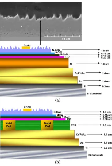
The schematic cross-sectional representations of the struc-tures of InGaN–GaN VLEDs we proposed are shown in Fig. 1(a) with an Al mirror and Fig. 1(b) with an ODR com-posed of TiO –SiO multilayer stake. The prepared GaN LED wafer consists of a 50-nm-thick GaN nucleation layer grown at 550 C, a 3- m-thick Si-doped n-GaN buffer layer grown at 1050 C, an unintentionally doped InGaN–GaN multiple quantum-well (MQW) active region grown at 770 C, a 50-nm-thick Mg-doped p-AlGaN electron blocking layer grown at 1050 C, a 0.15- m-thick Mg-doped p-GaN contact layer grown at 1050 C, and a Si-doped n In Ga N–GaN short period superlattice (SPS) structure. The MQW ac-tive region consists of five periods of 3-nm/7-nm-thick In Ga N–GaN quantum-well layers and barrier layers. By performing a split-wafer experiment, the original InGaN–GaN MQW LED wafer with backside polished sapphire substrate was cleaved into the size of cm . A transparent conducting layer composed of indium–tin–oxide (ITO) with thickness 300 nm was first deposited onto the p-GaN sur-face of the wafer by electron beam evaporation for current
566 IEEE PHOTONICS TECHNOLOGY LETTERS, VOL. 19, NO. 8, APRIL 15, 2007
Fig. 1. Schematic diagram of a VLED structure (a) with Al mirror and rough-ness (b) TiO –SiO ODR and roughrough-ness. Inset in (a) shows the SEM image of surface roughness with PEC process.
spreading. For the VLED structure with an ODR, since the ODR is nonconducting, we need to integrate some conducing channels inside the ODR to contact with ITO for vertical cur-rent spreading. The procedure was described as follows. First, an array of line of resistance posts with diameter 50 m and height 7 m, defined by the standard photolithographic process and formed on an ITO surface. Second, the designed ODR was directly deposited on the defined post array by electron beam evaporation. Third, those posts were moved away by a lift-off procedure. Finally, the forming holes inside the ODR were filled with Cr–Pt–Au to serve as conducing channels or p-GaN metal contacts. We also deposited a layer of Au with thickness of 1.4 m on the ODR surface for proceeding with the wafer bonding process. For the VLED structure with an Al mirror, the sample was prepared rather straightforwardly by depositing an Al layer with thickness of 1 m on the ITO surface and a Au layer with thickness of 1.4 m on the surface of the forming an Al layer. Both types of samples were then bonded onto a Ti–Au-coated p-type conducting Si substrate by a commercial SUSS SB6e wafer bonder with a bonding temperature of 340 C and a bonding pressure of 17 kg/cm for 140 min. After that, the wafer-bonded samples were taken to undergo the laser lift-off process. A KrF excimer laser at wavelength of 248 nm with a pulsewidth of 25 ns was used to
Fig. 2. Plain view photomicrograph of the LED with TiO –SiO ODR in op-eration.
remove the sapphire substrate. The incident laser with a beam size of 1.2 mm 1.2 mm was incident from the polished back-side of the sapphire substrate onto the sapphire–GaN interface to decompose GaN into Ga and N . In this process, the beam size of the KrF laser was larger than our desired size (1 mm 1 mm) of LEDs. Therefore, the laser irradiation on the interface of sapphire and GaN was uniform. After the sapphire substrate was removed by the excimer laser, the sapphire-removed sam-ples were dipped into H SO solution to remove the residual Ga on the n-GaN. In order to thin out the revealed n-GaN, the whole sapphire-removed samples were etched by inductively coupled plasma reactive ion etching and the associated mesas were etched further down to the ODR interface for single-chip isolation. To further increase the light extraction efficiency, the n-GaN surfaces of the samples were roughened through a photo-electrochemical (PEC) etching of the n-GaN surface using a UV lamp and a dilute aqueous solution of KOH [11]. The voltage bias was fixed at a positive 10 V on the n-GaN surface, and exposure under 400-W Hg lamp illumination. Then the oxide layer was removed in a diluted HCl solution HCl:H O . Finally, a patterned Cr–Au electrode were deposited on n-GaN as the n-type contact layer.
The designed ODR is composed of 14 pairs of TiO –SiO that were evaporated onto an ITO layer by an E-beam evapo-rator [10]. For the detailed band structure calculation and geom-etry design, refer to [10]. Fig. 2 shows a plane photomicrograph view of our thin-film VLED with the designed ODR in opera-tion. The hexagonal array of dark holes made of Cr–Pt–Au are the fabricated conducting channels and located just below the ITO layer. We can clearly observe that those conducting metal holes are rather absorptive compared with the ODR. This result is consistent with the prediction on the superior reflectance of the ODR over its counterpart of metal mirrors.
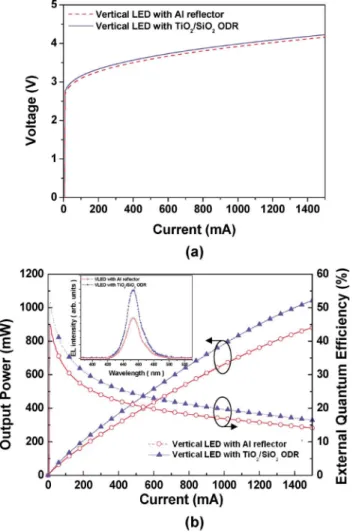
Fig. 3(a) shows the forward current–voltage ( – ) curves for the thin-film VLED with ODR and the one with Al mirror. It was found that the measured forward voltages under injec-tion current 350 mA at room temperature for the LED with TiO –SiO ODR and the LED with Al mirror were approxi-mately 3.52 and 3.46 V, respectively. The slightly higher for-ward voltage of the LED with TiO –SiO ODR than that with Al mirror can be attributed to additional thermal processes during the ODR deposition. We believe that ITO/SPS layer interfa-cial mixing could result in a higher specific contact resistance and hence could raise the LED operation voltage. In addition, the current spreading via the conducting channels inside the ODR could cause the forward voltage to be slightly higher.
HUANG et al.: HIGH-PERFORMANCE GaN-BASED VLEDs WITH TIO –SIO ODR AND n-GaN ROUGHNESS 567
Fig. 3. (a)I–V and (b) intensity–current (L–I) and EQE versus forward dc current for the LED with TiO –SiO ODR and roughness, and for the LED with Al reflector and roughness fabricated in this letter. The inset shows the room-temperature EL spectrums at a driving current of 350 mA.
Fig. 3(b) shows light–output power and external quantum ef-ficiency (EQE) versus forward dc current for the LED with TiO –SiO ODR and the one with Al reflector are taken contin-uous-wave. At an injection current of 350 mA, the light–output power of the LED with TiO –SiO ODR and the LED with Al reflector were approximately 330 and 279 mW, respectively. The LED with TiO –SiO ODR increased the output power by a factor of 1.18, indicating that TiO –SiO ODR had higher re-flectance and better light extraction efficiency than Al mirror. The EQE varies in a similar manner as the output power with forward dc current. The EQE of the LED with TiO –SiO ODR is 1.16 times higher than that of the LED with Al reflector under all our measurement conditions. According to Fig. 3(b), at a driving current 350 mA, the EQEs for the LEDs with TiO –SiO ODR and the one with Al reflector are 26.7% and 23.0%, respec-tively. The inset of Fig. 3(b) shows the typical room-temperature
electroluminescence (EL) spectra of InGaN-based LEDs with TiO –SiO ODR and InGaN-based LEDs with Al reflector at a driving current of 350 mA; it shows that the InGaN-based MQW emission peaks of those two devices are both located at 455 nm. However, the EL intensity of the LEDs with TiO –SiO ODR was larger than that of the LEDs with Al reflector.
In summary, GaN-based thin-film VLEDs with TiO –SiO ODR and n-GaN roughness were designed and fabricated. At a driving current of 350 mA and with a chip size of 1 mm 1 mm, the light–output power and the EQE of the LED with TiO –SiO ODR reached 330 mW and 26.7%, which were in-creased by 18% and 16%, respectively, when compared with the results from the LED with Al mirror. Our work brings out a new structure with superior performance for the next generation of high-brightness InGaN–GaN LEDs.
ACKNOWLEDGMENT
The authors would like to thank Prof. K. M. Lau of Hong Kong University of Science and Technology and Prof. S. Y. Lin of RPI for useful discussions.
REFERENCES
[1] E. F. Schubert and J. K. Kim, “Solid-state light sources becoming smart,” Science, vol. 308, pp. 1274–1278, 2005.
[2] S. J. Chang, C. S. Chang, Y. K. Su, C. T. Lee, W. S. Chen, C. F. Shen, Y. P. Hsu, S. C. Shei, and H. M. Lo, “Nitride-based flip-chip ITO LEDs,”
IEEE Trans. Adv. Packag., vol. 28, no. 2, pp. 273–277, May 2005.
[3] C. F. Chu, F. I. Lai, J. T. Chu, C. C. Yu, C. F. Lin, H. C. Kuo, and S. C. Wang, “Study of GaN light-emitting diodes fabricated by laser lift-off technique,” J. Appl. Phys., vol. 95, pp. 3916–3922, 2004.
[4] T. Fuji, Y. Gao, R. Sharma, E. L. Hu, S. P. DenBaars, and S. Naka-mura, “Increase in the extraction efficiency of GaN-based light-emit-ting diodes via surface roughening,” Appl. Phys. Lett., vol. 84, pp. 855–857, 2004.
[5] J. K. Kim, T. Gessmann, H. Luo, and E. F. Schubert, “GaInN light-emitting diodes with RuO=SiO =Ag omni-directional re-flector,” Appl. Phys. Lett., vol. 84, pp. 4508–4510, 2004.
[6] Y. Fink, J. N. Winn, S. Fan, C. Chen, J. Michel, J. D. Joannopoulos, and E. L. Thomas, “A dielectric omnidirectional reflector,” Science, vol. 282, pp. 1679–1682, 1998.
[7] Y. S. Zhao, D. L. Hibbard, H. P. Lee, K. Ma, W. So, and H. Liu, “Efficiency enhancement of InGaN/GaN light-emitting diodes with a back-surface distributed bragg reflector,” J. Electronic Mater., vol. 32, pp. 1523–1526, 2003.
[8] J. D. Joannopoulos, R. Meade, and J. N. Winn, Photonic Crystals:
Molding the Flow of Light. Princeton, NJ: Princeton Univ. Press, 1995.
[9] C. H. Lin, J. Y. Tsai, C. C. Kao, H. C. Kuo, C. C. Yu, J. R. Lo, and K. M. Leung, “Enhanced light output in InGaN-based light-emitting diodes with omnidirectional one-dimensional photonic crystals,” Jpn.
J. Appl. Phys., vol. 45, pp. 1591–1593, 2006.
[10] C. H. Lin, C. F. Lai, T. S. Ko, H. W. Huang, H. C. Kuo, Y. Y. Hung, K. M. Leung, C. C. Yu, R. J. Tsai, C. K. Lee, T. C. Lu, and S. C. Wang, “Enhancement of InGaN–GaN indium–tin–oxide flip-chip light-emitting diodes with TiO –SiO multilayer stack omnidirec-tional reflector,” IEEE Photon. Technol. Lett., vol. 18, no. 19, pp. 2050–2052, Oct. 1, 2006.
[11] C.-F. Lin, Z.-J. Yang, J.-H. Zheng, and J.-J. Dai, “High-efficiency InGaN light-emitting diodes via sidewall selective etching and oxida-tion,” J. Electrochem. Soc., vol. 153, no. 1, pp. G39–G43, 2006.