Fabrication and characterization of three-dimensional all metallic photonic crystals
for near infrared applications
Yu-Lin Yang, Fu-Ju Hou, Shich-Chuan Wu, Wen-Hsien Huang, Ming-Chih Lai, and Yang-Tung Huang
Citation: Applied Physics Letters 94, 041122 (2009); doi: 10.1063/1.3075056
View online: http://dx.doi.org/10.1063/1.3075056
View Table of Contents: http://scitation.aip.org/content/aip/journal/apl/94/4?ver=pdfcov Published by the AIP Publishing
Articles you may be interested in
Thermal emission at near-infrared wavelengths from three-dimensional copper photonic crystals J. Appl. Phys. 110, 044909 (2011); 10.1063/1.3625263
Three-dimensional metallic photonic crystals fabricated by soft lithography for midinfrared applications Appl. Phys. Lett. 88, 181112 (2006); 10.1063/1.2201621
Optical tuning of three-dimensional photonic crystals fabricated by femtosecond direct writing Appl. Phys. Lett. 87, 091117 (2005); 10.1063/1.2037862
Fabrication of three-dimensional photonic crystal with alignment based on electron beam lithography Appl. Phys. Lett. 85, 5037 (2004); 10.1063/1.1825623
Transmission characterization of drilled alternating-layer three-dimensional photonic crystals J. Appl. Phys. 93, 8848 (2003); 10.1063/1.1569996
This article is copyrighted as indicated in the article. Reuse of AIP content is subject to the terms at: http://scitation.aip.org/termsconditions. Downloaded to IP: 140.113.38.11 On: Wed, 30 Apr 2014 15:33:08
Fabrication and characterization of three-dimensional all metallic photonic
crystals for near infrared applications
Yu-Lin Yang,1Fu-Ju Hou,2Shich-Chuan Wu,2,a兲Wen-Hsien Huang,2Ming-Chih Lai,2and Yang-Tung Huang1
1
Department of Electronic Engineering and Institute of Electronics, National Chiao-Tung University, 1001 Ta-Hsueh Road, Hsinchu 300, Taiwan
2
National Nano Device Laboratory, 26 Prosperity Road I, Science-based Industrial Park, Hsinchu 300, Taiwan
共Received 28 October 2008; accepted 6 January 2009; published online 29 January 2009兲
Three-dimensional all metallic photonic crystals with a feature size of 0.20 m were fabricated using electron-beam lithography with the photoresist of hydrogen silesquioxane. This process method has high compatibility with the fabrication of damascene copper interconnections and also simplifies the whole process flow. The dependence of the complete photonic band gaps on polarization was experimentally observed and compared with the simulation results. The band edge for the four-layer lattice was found at a wavelength of around 0.80 m in normal incidence. © 2009 American Institute of Physics.关DOI:10.1063/1.3075056兴
In recent years, three-dimensional共3D兲 photonic crystals 共PCs兲 have attracted great attention since they have the abil-ity to control the flow of light omnidirectionally for a spe-cific range of frequencies, which is so-called a complete pho-tonic band gap 共PBG兲. Among a variety of the proposed 3D structures, the woodpile structure1has been explored for its relatively large PBG and simple design rules of introducing the intentional defects.2–4 This structure has been success-fully realized with dielectric materials by some state-of-the-art technologies, such as wafer bonding,5 direct laser writing,6,7 and atomic layer deposition.8 For their metallic counterpart, most demonstrations are limited to the 3D me-tallic PCs created by performing the different metallization techniques on the 3D dielectric templates.9–12However, fab-ricating a 3D all metallic PC with a feature size of submicron in a large area is still a challenge due to its complex process-ing steps.
One of the promising features for metallic PCs is the capability of tailoring their thermal emission spectra. In the range of PBG, thermal emission from the 3D metallic PCs is suppressed, and narrow band emission is observed at the wavelengths near the photonic band edges.13,14These metal-lic PCs have been demonstrated as light sources with high electrical-to-optical conversion efficiency. To achieve emis-sion at shorter wavelengths, the feature sizes of the 3D lat-tices are necessary to be scaled down for shifting the band edges to higher frequencies. In addition, choosing appropri-ate mappropri-aterials to construct metallic PCs plays an important role as well. For some metals available in standard integrated circuit 共IC兲 technology, severe intrinsic absorption at near infrared or visible wavelengths is an obstacle to scale the band edge down. It is essential to adopt a metal of high plasma frequency for holding the linear scaling rule of the band edge positions.9
In this letter, copper was selected as the material to form the 3D lattice with a feature size of 0.20 m for its desirable optical properties at near infrared wavelengths and high
compatibility with the fabrication of damascene copper interconnections.9,15To simplify the complexity of processes, the electron-beam 共e-beam兲 lithography was used to realize the 3D all copper PCs with the photoresist of hydrogen silesquioxane共HSQ兲. Experimentally, the complete photonic band edge was observed at a wavelength of around 0.80 m. Its dependence on polarization of incident light will be discussed.
The 3D PCs that we realized are the four-layer woodpile structure, similar to face-centered-tetragonal 共fct兲 lattice symmetry. For the ideal fct lattice, they consist of parallel copper rods with a pitch of a in each layer, where a = 0.50 m in this report. The orientation of rods in one layer is perpendicular to that in the adjacent layers. The position of the rods in one layer is shifted by a/2 with respect to that in the alternate layers. As shown in Fig. 1, practically, the cop-per rods in the third and fourth layers are shifted by
a兲Author to whom correspondence should be addressed. Electronic mail:
FIG. 1. 共a兲 A SEM image of the HSQ pattern formed after the process of e-beam lithography.关共b兲–共d兲兴 SEM images of the 3D all copper PCs from the tilted, top, and cross-sectional views, respectively. The width and height of copper rods are about 200 and 180 nm, respectively. The rod-to-rod spacing is about 500 nm. This structure was built with four layers to form one unit cell of a fct-like lattice. The deviation from the ideal fct lattice is due to the misalignment of copper rods in the third and fourth layers.
APPLIED PHYSICS LETTERS 94, 041122共2009兲
0003-6951/2009/94共4兲/041122/3/$25.00 94, 041122-1 © 2009 American Institute of Physics This article is copyrighted as indicated in the article. Reuse of AIP content is subject to the terms at: http://scitation.aip.org/termsconditions. Downloaded to IP:
0.05 m with respect to the ideal position. The 3D copper PCs were fabricated layer-by-layer using the process of e-beam lithography. First, the HSQ film 共FOx-15, Dow Corning兲 was spin-coated on a silicon wafer as a high-resolution negative photoresist for the e-beam lithography 共Weprint 200 type, Lecia兲. After the processes of exposure and development, the grating pattern was formed as shown in Fig.1共a兲. The HSQ pattern was annealed at 400 ° C for 1 h in order to resist the following process of chemical-mechanical polishing共CMP兲. The 25 nm thick tantalum and 50 nm thick copper seed layers were then deposited on the resulting HSQ pattern by the physical vapor deposition sys-tem. This step was followed by the processes of copper elec-troplating for filling the HSQ trenches and CMP for remov-ing excess copper and tantalum on the top of the HSQ trenches. The same processes were repeated layer-by-layer as desired. After this HSQ mold was removed by a solution of dilute hydrofluoric acid, the entire fabrication processes were completed. This etchless method is compatible with the cop-per interconnect technology and simplifies the whole process flow owing to omission of processes of extra depositing and etching intermetal dielectric layers, which allows easier for-mation of patterns with smaller feature sizes 共⬉100 nm兲.16 The HSQ layers were used as the photoresist of the e-beam writer as well as the sacrificial dielectric mold for the metal-lic PCs. The scanning electron microscope共SEM兲 images of the fabricated 3D all copper PCs are shown in Figs. 1共b兲–1共d兲. The width and height of the fabricated copper rods are about 0.20 and 0.18 m, respectively. The overall sample area is 5⫻5 mm2.
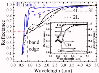
To observe the PBG behaviors of the fabricated 3D all copper PCs, the Fourier transform infrared 共FTIR兲 micro-scope共Hyperion 2000, Bruker兲 was used to measure the re-flectance spectra for the two-, three-, and four-layer struc-tures. The reflectance was obtained by normalizing the measured results taken from the fabricated samples to that from the uniform gold mirror. In Fig.2, the measured reflec-tance spectra in the case of unpolarized incident light are shown and compared with the simulation results for s- and p-polarization, which were taken for an ideal four-layer fct lattice with the same dimensions as the practical one. This
simulation was performed by the 3D finite-difference time-domain method with the commercial software 共RSOFT兲, and
the wavelength-dependent refractive indices17–19 were used. As shown in Fig.2, the PBG develops gradually as the num-ber of layers increases. For the four-layer lattice, the mea-sured reflectance keeps very high values 共⭌0.95兲 for wave-lengths longer than 2.95 m due to the typical PBG effect of the metallic PCs, exhibits a dip at a wavelength of about 1.20 m, and decreases sharply to 0.31 at a wavelength of 0.60 m. The sharp drop for the wavelengths shorter than 0.60 m is caused by the increase in the absorption of copper17 and the transmission for the waveguide effect with the cutoff wavelength of 0.60 m.20 The photonic band edge, where reflectance is defined as 0.5, was found at a wavelength of about 0.80 m. The measured results show the similar trend to the simulation results except for the lower reflectance vales at wavelengths near the band edge. The dips in the simulation results at a wavelength of around 0.80 m correspond to the narrow transmission and absorp-tion peaks. In the measurements, these dips are not clearly observed, which might be due to the deviations between the ideal lattice and the actual samples. Possible causes of the dip at the wavelength of about 1.20 m are as follows. First, copper is of intrinsic absorption in the wavelength ranges from about 1.30 to 1.70 m, as shown in the inset of Fig.2. The reflectance R of the copper and tantalum films was cal-culated as R =关共n−1兲2+ k2兴/关共n+1兲2+ k2兴, where n and k are the real and imaginary parts of the wavelength-dependent refractive index of metal,17 respectively. The absorptance A was assumed to be 1 − R 共for no transmission兲. Second, ow-ing to the limited acceptance angle of the objective lens equipped in the FTIR microscope, only the portion of the Rayleigh scattered light from the 3D lattices captured by the objective lens contributes to the measured signals, leading to the discrepancy between the measured and simulation results.10–12It is inferred that this loss of magnitude becomes more significant as the number of PC layers increases and wavelengths of measured incident light are shorter. In com-parison with the copper-coated counterpart reported by Tal et al.,12 our structure has advantages in higher compatibility with the standard IC technology and capability for designing more functionalities in one chip 共larger lateral areas兲 and with a smaller feature size for achieving the photonic band edge to a shorter wavelength.
To obtain insight into the characterization of the 3D cop-per PCs, the reflectance spectra for s- and p-polarized inci-dent light were measured and shown in Fig. 3. The reflec-tance spectra are depicted as a function of number of layers. Figure 3共a兲 shows that measured reflectances for different layer structures are roughly identical for s-polarization. This is because the waveguide cutoff effect20 plays an important role for this case. The slight drop appearing at a wavelength of about 2.29 m for the four-layer lattice, which was not predicted from the simulation results, may stem from the imperfections in the sample. On the other hand, for p-polarization, the band edges are shifted to the shorter wavelengths when the number of layers increases, as shown in Fig.3共b兲. This is the evidence for the development of the complete band gap for the woodpile PCs. It is noted that the dip at a wavelength of about 1.20 m in the measured spec-trum for the four-layer lattice is much deeper than that from the simulation results. This may be attributed to the fact that
FIG. 2. 共Color online兲 Simulated and measured reflectance spectra for the 3D copper PCs with different number of layers. The unpolarized light is incident along the z-axis. The band edge is shown at a wavelength of about 0.80 m for the four-layer PC. In the inset, the calculated reflectance and absorptance spectra of copper and tantalum films共their thicknesses are as-sumed to be much larger than skin depths兲 are shown, respectively.
041122-2 Yang et al. Appl. Phys. Lett. 94, 041122共2009兲
This article is copyrighted as indicated in the article. Reuse of AIP content is subject to the terms at: http://scitation.aip.org/termsconditions. Downloaded to IP: 140.113.38.11 On: Wed, 30 Apr 2014 15:33:08
for the p-polarized incident light, the longer penetration length into the 3D copper PCs leads to stronger Rayleigh scattering at large angles and lower measured magnitude de-tected by the FTIR microscope. Consequently, the measured reflectance spectra represent the combined results of the loss of reflected signals from samples and the PBG effect of the 3D metallic PCs.
To verify the properties of the complete PBG, the tilted-angle measurements were performed with the grazing tilted-angle objective 共Bruker兲 equipped in the FTIR microscope, as shown in Fig.4. The angles of grazing incidence are between 52.2° and 84.2° off the normal to the surface of the sample, as shown in the inset of Fig.4. The measured results show that the reflectance still keeps high values共⭌0.80兲 at wave-lengths longer than 3.25 m for both polarizations and de-creases sharply at shorter wavelengths. The locations of band edges are shifted to the longer wavelengths owing to the shortage of the number of layers.21In addition, the tantalum layers adhered on the side walls of copper rods in each layer
may play an important role for the results of grazing-angle measurements. Tantalum is absorptive at wavelengths shorter than 1.50 m as shown in the inset of Fig.2. The incident light at such large angles experiences more tantalum, which leads to the more significant drop in reflectance. Therefore, for the four-layer structure, the edge of the complete PBG is at a wavelength of around 1.50 m in grazing-angle inci-dence, implying that the 3D copper PCs can be used for the near infrared applications.
In summary, the e-beam lithography with the photoresist of the HSQ has been adopted to create the 3D all copper PCs with a feature size of 0.20 m. This approach is compatible with the standard IC technology and also simplifies the whole process flow. Experimental results show that the pho-tonic band edge is located at a wavelength of around 0.80 m in normal incidence. For applications in the visible wavelength range, we offer a possible method to accomplish all metallic PCs with smaller feature sizes.
The authors would like to thank the staff at National Nano Device Laboratory for assistance in fabrication of samples. Yu-Lin Yang also thanks Professor Shawn-Yu Lin of Rensselaer Polytechnic Institute for valuable discussions about the characterization of the 3D metallic PCs. This work was supported in part by National Science Council under Contract No. 96-2221-E-492-006 and by National Nano De-vice Laboratory for the project of nanometer-scaled 3D metal PCs.
1K. M. Ho, C. T. Chan, C. M. Soukoulis, R. Biswas, and M. Sigalas,Solid
State Commun. 89, 413共1994兲.
2S. Ogawa, M. Imada, S. Yoshimoto, M. Okano, and S. Noda,Science 305,
227共2004兲.
3S. Kawashima, L. H. Lee, M. Okano, M. Imada, and S. Noda, Opt.
Express 13, 9774共2005兲.
4A. Chutinan and S. John,Opt. Express 14, 1266共2006兲.
5S. Noda, K. Tomoda, N. Yamamoto, and A. Chutinan,Science 289, 604
共2000兲.
6M. Deubel, G. V. Freytmann, M. Wegener, S. Pereira, K. Busch, and C. M.
Soukoulis, Nature共London兲 3, 444 共2004兲.
7W. Haske, V. W. Chen, J. M. Hales, W. Dong, S. Barlow, S. R. Marder,
and J. W. Perry,Opt. Express 15, 3426共2007兲.
8J.-H. Lee, W. Leung, J. Ahn, T. Lee, I.-S. Park, K. Constant, and K.-M.
Ho,Appl. Phys. Lett. 90, 151101共2007兲.
9S. Y. Lin, D.-X. Ye, T.-M. Lu, J. Bur, Y. S. Kim, and K. M. Ho,J. Appl.
Phys. 99, 083104共2006兲.
10J.-H. Lee, C.-H. Kim, Y.-S. Kim, K.-M. Ho, and C. H. Oh,Appl. Phys.
Lett. 88, 181112共2006兲.
11V. Mizeikis, S. Juodkazis, R. Tarozaite, J. Juodkazyte, K. Juodkazis, and
H. Misawa,Opt. Express 15, 8454共2007兲.
12A. Tal, Y.-S. Chen, H. E. Williams, R. C. Rumpf, and S. M. Kuebler,Opt.
Express 15, 18283共2007兲.
13S. Y. Lin, J. Moreno, and J. G. Fleming,Appl. Phys. Lett. 83, 380共2003兲. 14J.-H. Lee, Y.-S. Kim, K. Constant, and K.-M. Ho,Adv. Mater.共Weinheim,
Ger.兲 19, 791共2007兲.
15T. A. Walsh and S.-Y. Lin, IEEE Trans. Electron Devices 55, 1101共2008兲. 16D. P. Mancini, K. A. Gehoski, E. Ainley, K. J. Nordquist, D. J. Resnick, T.
C. Bailey, S. V. Screenivasan, J. G. Ekerdt, and C. G. Willson,J. Vac. Sci. Technol. B 20, 2896共2002兲.
17E. D. Palik, Handbook of Optical Constants of Solids共Academic, London,
1985兲, p. 285.
18M. A. Ordal, L. L. Long, R. J. Bell, S. E. Bell, R. R. Bell, R. W.
Alex-ander, Jr., and C. A. Ward, Appl. Opt. 22, 1099共1983兲.
19I. El-Kady, M. M. Sigalas, R. Biswas, K. M. Ho, and C. M. Soukoulis,
Phys. Rev. B 62, 15299共2000兲.
20Z.-Y. Li, I. El-Kady, K.-M. Ho, S. Y. Lin, and J. G. Fleming, J. Appl.
Phys. 93, 38共2003兲.
21J. G. Fleming, S. Y. Lin, I. El-Kady, R. Biswas, and K. M. Ho,Nature
共London兲 417, 52共2002兲.
FIG. 3. 共Color online兲 Simulated and measured reflectance spectra for the 3D copper PCs with numbers of layers. The共a兲 s- and 共b兲 p-polarized light is incident along the z-axis. Here, s- and p-polarization are defined as the electric fields of incident light parallel and perpendicular to the extension direction of copper rods in the outermost layer, respectively.
FIG. 4.共Color online兲 Measured reflectance spectra taken at grazing angles for the 3D copper PCs with number of layers. The s- and p-polarized light is incident off the normal at 52.2° to 84.2°, respectively. The sketch of the experimental configuration is shown in the inset.
041122-3 Yang et al. Appl. Phys. Lett. 94, 041122共2009兲
This article is copyrighted as indicated in the article. Reuse of AIP content is subject to the terms at: http://scitation.aip.org/termsconditions. Downloaded to IP: 140.113.38.11 On: Wed, 30 Apr 2014 15:33:08