Edge quantum yield in n-channel metal-oxide-semiconductor field-effect transistor
Ting-Kuo Kang, K. C. Su, Yih J. Chang, Ming-Jer Chen, and Shih-Hsin YehCitation: Journal of Applied Physics 96, 1743 (2004); doi: 10.1063/1.1751627 View online: http://dx.doi.org/10.1063/1.1751627
View Table of Contents: http://scitation.aip.org/content/aip/journal/jap/96/3?ver=pdfcov
Published by the AIP Publishing
Articles you may be interested in
Modeling random telegraph signals in the gate current of metal–oxide–semiconductor field effect transistors after oxide breakdown
J. Appl. Phys. 94, 703 (2003); 10.1063/1.1579134
Analytical approach to integrate the different components of direct tunneling current through ultrathin gate oxides in n-channel metal–oxide–semiconductor field-effect transistors
J. Appl. Phys. 93, 1064 (2003); 10.1063/1.1527710
Electrical effects of a single stacking fault on fully depleted thin-film silicon-on-insulator P-channel metal–oxide–semiconductor field-effect transistors
J. Appl. Phys. 91, 420 (2002); 10.1063/1.1417995
Observation of double peak in the substrate current versus gate voltage characteristics of n-channel metal–oxide–semiconductor field effect transistors
Appl. Phys. Lett. 78, 2238 (2001); 10.1063/1.1361279
Two dimensional dopant and carrier profiles obtained by scanning capacitance microscopy on an actively biased cross-sectioned metal–oxide–semiconductor field-effect transistor
J. Vac. Sci. Technol. B 18, 549 (2000); 10.1116/1.591230
[This article is copyrighted as indicated in the article. Reuse of AIP content is subject to the terms at: http://scitation.aip.org/termsconditions. Downloaded to ] IP: 140.113.38.11 On: Thu, 01 May 2014 04:16:21
Edge quantum yield in
n
-channel metal-oxide-semiconductor
field-effect transistor
Ting-Kuo Kang,a) K. C. Su, and Yih J. Chang
Reliability Engineering Department, United Microelectronics Corporation, Science-Based Industrial Park, Hsin-Chu City, Taiwan, Republic of China
Ming-Jer Chen and Shih-Hsin Yeh
Department of Electronics Engineering, National Chiao-Tung University, Hsin-Chu, Taiwan, Republic of China
共Received 23 June 2003; accepted 26 March 2004兲
The quantum yield of impact ionization is performed on an n-channel metal-oxide-semiconductor field-effect transistor 共n-MOSFET兲 by a carrier separation measurement. When the n-MOSFET is biased in accumulation, the carrier separation measurement demonstrates that the gate current mainly originates from the electrons injected into the underlying drain/source overlap regions. The measured substrate current is due to excess holes originating from the impact ionization of the injected electrons in the overlap regions. Therefore, the quantum yield in the overlap regions can be determined by the ratio of the substrate current to the gate current. It is well matched with the theoretical calculation of quantum yield. © 2004 American Institute of Physics.
关DOI: 10.1063/1.1751627兴
p-channel metal-oxide-semiconductor field-effect
tran-sistors 共p-MOSFETs兲 are generally used in the study of quantum yield of impact ionization for electrons in silicon. The quantum yield experiment by a carrier separation con-figuration can essentially assess the energy of electrons in-jected into the gate oxide.1Such an experiment on n⫹-poly gate p-MOSFETs in the stress-induced leakage current mode has evidenced the inelastic trap-assisted tunneling mecha-nism of injected electrons.2 For p⫹-poly gate p-MOSFETs the inelastic trap-assisted tunneling mechanism in the stress-induced leakage current mode has also been proposed.3 Re-cently, it has been reported that quantum yield experiments can be performed directly on a triple well structure of
n-channel metal-oxide-semiconductor field-effect transistors
共n-MOSFETs兲.4
Therefore, this work focuses on the gate-to-drain/source overlap regions of an n-MOSFET.
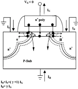
The n-MOSFET with n⫹-poly gate was fabricated in a state-of-the-art 0.15 m process. The gate width/length as-pect ratio is 100m/0.13m. In this process, the gate oxide was thermally grown in dilute oxygen ambient. The physical gate oxide thickness was determined to be 2.6 nm by using an I – V fitting method.5A schematic illustration of the ex-perimental set-up of the carrier separation measurement is shown in Fig. 1.
Figure 2 depicts the dependence of the measured gate current IG, drain current ID, source current IS, and
sub-strate current IB on the gate voltage VG in accumulation.
This figure concludes three points. First, ID⬇ISindicates the
symmetry of experimental set-up. Second, IG⬇ID⫹IS satis-fies in the direct tunneling regime (⫺4 V⬍VG⬍0). It
effec-tively points out that the electron current paths are mainly from the gate terminal to the drain and source terminals, as
plotted in Fig. 1. Third, since the substrate current has a negative sign, this indicates that the impact ionization in-duced holes flow down into the substrate. However, these holes could be either generated in the overlap regions or in the substrate region.
The quantum yield experiment gives strong evidence to the validity of the impact ionization in the overlap regions. The quantum yield␥, which is determined by the ratio of the substrate current IB to the gate current IG, is described as a
function of the electron energy Ee. Assuming the electron
energy Ee is equal to the potential drop across the oxide
(Ee⫽qVox), featuring quasiballistic transport. In the
gate-to-overlap regions, the oxide voltage Vox is expressed as
a兲Electronic mail: kevinគ[email protected]
FIG. 1. A schematic illustration of the quantum yield experiment in the
n-MOSFET. The closed and open circles represent electrons and holes,
re-spectively. The dotted lines represent the depletion region edges.
JOURNAL OF APPLIED PHYSICS VOLUME 96, NUMBER 3 1 AUGUST 2004
1743
0021-8979/2004/96(3)/1743/2/$22.00 © 2004 American Institute of Physics
[This article is copyrighted as indicated in the article. Reuse of AIP content is subject to the terms at: http://scitation.aip.org/termsconditions. Downloaded to ] IP: 140.113.38.11 On: Thu, 01 May 2014 04:16:21
VG– Vd, where Vd is the overlap band bending. Vd can be
obtained by using a depletion approximation. Due to the co-incidence between the resulting ratio␥in the overlap regions and the quantum yield theory,6 as shown in Fig. 3, it is named as ‘‘edge quantum yield’’ in this work. On the other hand, the possibility of impact ionization in the substrate region is also considered. Similarly, the Vox in the
gate-to-substrate region is expressed as VG-Eg/q, where Eg/q is the
silicon band gap in volts. The discrepancy between the re-sulting ratio␥in the substrate region and the quantum yield theory,6especially at⫺3 V⬍VG⬍0, is shown in Fig. 3. It is
reasonable to infer that the impact ionization in the substrate region is negligible due to a small channel length.
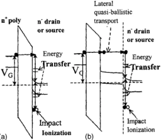
To further interpret the edge quantum yield, the energy-band diagram in the overlap regions is depicted as follows. Figure 4共a兲 shows how the injected electrons from the gate to drain/source overlap regions transfer energy via impact ion-ization. A more interesting phenomenon is highlighted in Fig. 4共b兲 for the electrons injected into the substrate. We assume that since a small channel length allows lateral qua-siballistic behavior, the energetic electrons will traverse to the drain/source collectors without energy loss. When these ‘‘hot’’ electrons enter the overlap depletion regions, they would transfer the energy via impact ionization to become ‘‘cold’’ electrons eventually.
In conclusion, the edge quantum yield experiment has been successfully performed on an n-MOSFET and its physi-cal basis has been clarified. The experimental data are in excellent agreement with theoretical calculation.
The authors would like to thank Mingte Lin, Oswin Lo, Rita Chen, Charles Jiang, and Michelle Chiang for their use-ful discussions. Also, the authors are grateuse-ful to Dr. Thomas Huttner and Dr. Michael Rohner of Infineon Technologies for their valuable comments.
1
C. Chang, C. Hu, and R. W. Brodersen, J. Appl. Phys. 57, 302共1985兲. 2S. Takagi, N. Yasuda, and A. Toriumi, IEEE Trans. Electron Devices 46,
335共1999兲.
3A. Ghetti, M. Alam, J. Bude, D. Monroe, E. Sangiorgi, and H. Vaidya, IEEE Trans. Electron Devices 47, 1341共2000兲.
4
A. S. Spinelli, D. Ielmini, A. L. Lacaita, A. Sebastiani, and G. Ghidini, in Proceedings of the International Reliability Physics Symposium (IRPS) Dallas, Texas共IEEE, New York, 2003兲, p. 412.
5L. F. Register, E. Rosenbaum, and K. Yang, Appl. Phys. Lett. 74, 457 共1999兲.
6
R. C. Alig, S. Bloom, and C. Struck, Phys. Rev. B 22, 5565共1980兲.
FIG. 2. Four terminal currents of the n-MOSFET are measured in accumu-lation. The polarity of the substrate current IBis especially pointed out.
FIG. 3. Quantum yield,␥(⫽IB/IG), is described as a function of the
elec-tron energy Ee. The closed circles and squares represent the quantum yield
in the overlap regions and the substrate region, respectively.
FIG. 4. Energy-band diagram in the overlap regions is given for共a兲 n⫹-poly gate/n⫺-drain or source共b兲 n⫹-poly gate/p-substrate/n⫺-drain or source.
1744 J. Appl. Phys., Vol. 96, No. 3, 1 August 2004 Kanget al.
[This article is copyrighted as indicated in the article. Reuse of AIP content is subject to the terms at: http://scitation.aip.org/termsconditions. Downloaded to ] IP: 140.113.38.11 On: Thu, 01 May 2014 04:16:21