0925-9635/03/$ - see front matter䊚 2003 Elsevier Science B.V. All rights reserved. doi:10.1016/S0925-9635(03)00173-0
Growth and field emission of carbon nanofibers on electroless Ni–P alloy
catalyst
Ting-Kan Tsai
a,b,*, Chia-Chih Chuang , Chuen-Guang Chao , Wei-Long Liu
c a bDepartment of Materials Science and Engineering, National Chiao Tung University, Hsinchu 300, Taiwan, ROC a
Department of Materials Science and Engineering, National Huwei Institute of Technology, Huwei, Yunlin 632, Taiwan, ROC b
Department of Materials Science and Engineering, National Tsing Hua University, Hsinchu 300, Taiwan, ROC c
Received 17 July 2002; received in revised form 15 April 2003; accepted 21 April 2003
Abstract
Carbon nanofibers (CNFs) were grown on a Ni–P alloy catalyst deposited on a silicon substrate in a microwave heating
chemical vapor deposition system with methane gas at 650 8C. The Ni–P alloy catalyst films with various thicknesses were produced using an electroless plating nickel technique. The nanosized clusters on the clustered surface of the Ni–P alloy catalyst film directly provided the nucleation sites for CNFs without any pretreatment before the growth of the CNFs. The CNFs grown on the Ni–P alloy catalyst showed random orientation and it composed of parallel graphite planes with defects tilted from their axis. Field emission measurement indicated that the Ni–P catalyzed-CNFs exhibited excellent field emission properties. The diameter, growth rate and field emission properties show a strong correlation with the thickness of the Ni–P alloy catalyst film.
䊚 2003 Elsevier Science B.V. All rights reserved.
Keywords: Carbon nanofibers; Chemical vapor deposition; Field emission; Ni–P alloy
1. Introduction
Carbon nanofibers(CNFs), sometimes known as
car-bon filaments, are one kind of carcar-bon nanostructure. This kind of carbon nanostructure is clearly
distin-guished from carbon nanotubes (CNTs) in structural
conformation, although they often show great resem-blance in morphology. CNFs generally show a similar fullerence-like tip but with much disorder in the graphite crystallization all along the fiber w1x. In contrast, the CNTs have well-ordered graphite crystallinity w2x. Through careful control of the synthetic conditions including the chemical nature and physical conformation of catalyst, the composition and flow rate of hydrocar-bon gas reactant and reaction temperature, assorted CNF structures with various morphologies and different degrees of crystallinity can be produced w3x. CNFs growth on metal catalyst particles such as Fe, Co, Ni and their alloys from the decomposition of hydrocarbons
*Corresponding author. Tel.: 5-632-9643x621; fax: q886-5-636-1981.
E-mail address: [email protected](T.-K. Tsai).
have been known for a very long time w4–9x. In more recent years, vapor growth carbon fibers have attracted much attention, due to their extraordinary physical and chemical properties w10–12x. Efforts have been made to control the morphology and property of CNFs and improve the efficiency of the production processes
w2,13–18x.
Chemical vapor deposition (CVD) has been widely
used for CNTs, CNFs and other carbon nanostructures synthesis due to its high product yield and scale up capability. In the CVD method, the catalyst plays an important and indispensable role for the growth of CNFs. Chemical composition and particle size of the catalyst determine the structure, property and diameter of the CNFs. Many investigations have been developed to prepare the catalyst for depositing CNFs. Merkulov et
al. w16x evaporated Ni on (0 0 1) n-type Si by e-gun.
Shyu and Hong w17x deposited Fe–Ni with various components by e-beam evaporation. Chen et al. w18x
reduced foam Ni in flowing H at 300 8C and trans-2
formed it into a thin slice shape prior to the creation of the CNFs. Baker et al. w7x prepared copper–nickel powder by coprecipitation of the metal carbonates from
Table 1
The composition of plating solution and the experimental condition for electroless Ni–P plating
Chemicals Concentration(gyl)
NiSO Ø6H O4 2 20
NaH PO ØH O2 2 2 27
Na C H O Ø6H O2 4 4 4 2 16
Pb(NO )3 2 1 ppm
pH 4.2 Temperature 70 8C
mixed nitrate solutions using ammonium bicarbonate and a sequence complex treatment process including drying, calcining and reducing, etc. These methods need expensive equipment or complex processes for deposit-ing the metal catalyst film and for clusterdeposit-ing the metal catalyst film to nanoparticles.
The electroless plating nickel technique is a simple process with low cost and is easy to manage. This technique has been applied for ohmic contacts to silicon in semiconductor devices and for contact filling in very large scale integrated w19x for several years. However, there is little literature mentioned about electroless plating Ni deposited on substrates for fabricating CNFs. In this paper, we have deposited Ni–P alloy as catalyst on a silicon substrate using the electroless plating technique and a systematic study of the growth mor-phology and field emission property of CNFs from methane using Ni–P alloy catalyst in a microwave heating CVD system.
2. Experimental
A Ni–P alloy catalyst film was deposited using the electroless plating technique on a p-type(1 0 0) silicon
wafer(resistivity ;1–20 V cm). Prior to the electroless
plating process, it is necessary to sensitize and activate
the surface of silicon wafer using SnCl2 and PdCl2
solutions. The plating solution was composed of a
mixture of NiSO ,4 NaH PO ,2 2 Na C H O2 4 4 4 and
Pb(NO ) , where NiSO as the main nickel source,3 2 4 NaH PO is the reducing agent, Pb2 2 (NO ) is the stabi-3 2 lizing agent, and Na C H O is the buffer and complex2 4 4 4 agent for nickel. Since NaH PO was used as a reducer,2 2 the electroless plated nickel structures always incorpo-rated with phosphorus. The composition of the plating solutions and the experimental conditions are listed in Table 1. Thin Ni–P alloy catalyst films with various thickness were deposited onto the wafers for 10, 15 and 20 s.
A microwave heating CVD system has been utilized for growth of CNFs. The electroless Ni–P deposited-silicon substrate was placed on a ceramic holder, which was heated up to approximately 650 8C by controlling the microwave power. The temperature was detected by
a thermocouple contacted to the ceramic holder. CNFs were grown on the substrate using methane gas as the
source of carbon with flow rate 200 ccymin. The
pressure of the chamber was kept at atmosphere.
Transmission electron microscopy(TEM) was utilized
to observe the cross-sectional images of Ni–P alloy
catalyst films and atomic force microscopy (AFM) was
used to observe the surface morphology of the Ni–P alloy catalyst films. The morphology of the CNFs film deposited on the substrate was observed by field emis-sion scanning electron microscopy. The structure of the CNFs was characterized by high-resolution transmission
electron microscopy (HRTEM). Raman spectroscopy
was used to confirm the formation of graphitized CNFs. Field emission properties were measured by taking
electron emission current density–electric field (I–V)
curves using a Keithley 237 in a vacuum (10y6 Torr)
chamber at room temperature. A voltage up to 1100 V was applied and the distance between the indium–tin oxide film and the CNF’s tip is 180 mm.
3. Results and discussion
3.1. The morphology of the electroless Ni–P alloy catalyst film
Fig. 1 is a TEM cross-section image of the electroless Ni–P alloy catalyst film. The thickness of Ni–P alloy catalyst film, in Fig. 1a–c, was measured to be approx-imately 20, 30 and 40 nm in samples deposited for 10, 15 and 20 s, respectively. These samples with 20, 30 and 40 nm catalyst films are designated as sample A, sample Band sample C, respectively. It is clear that the thickness of the deposited catalyst film increases with the deposition time. When the deposition duration is extended, the Ni–P alloy catalyst film became dense from sparse and the surface of catalyst film became flatter gradually.
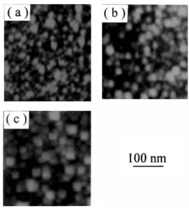
Fig. 2 is the AFM surface morphology image of the Ni–P alloy catalyst films. Fig. 2a–c show the surface morphologies of sample A, sample Band sample C, respectively. These figures show clearly that the clus-tered surface of the electroless Ni–P alloy catalyst film with different thickness consists of Ni–P alloy clusters with different size. When the deposited thickness is increased, the size of clusters is increased and the morphology of the clustered surface gradually becomes dense. The size of clusters in sample A, sample Band sample C are approximately 12–30, 26–37 and 35–42 nm, respectively. These nanosized clusters will directly provide the nucleation sites for CNFs without any pretreatment for catalyst film.
These above-mentioned results from TEM cross-sec-tion images and AFM surface morphology images indi-cate that the clustered surface morphology of the
Fig. 1. TEM cross-section images of the electroless Ni–P alloy cata-lyst film with various thicknesses. (a) Sample A was deposited for
10 s; (b) sample Bwas deposited for 15 s and (c) sample C was
deposited for 20 s.
Fig. 2. AFM surface morphology images of the electroless Ni–P alloy catalyst film with different size of clusters.(a) Sample A was
depos-ited for 10 s;(b) sample Bwas deposited for 15 s and (c) sample C
was deposited for 20 s.
electroless Ni–P alloy catalyst film is relevant to its thickness. The morphology of the catalyst film is known to play a critical role in CNF growth. So, the thickness of the Ni–P alloy catalyst film will affect the growth and the property of CNFs.
3.2. The growth of CNFs
Fig. 3 shows scanning electron microscopy (SEM)
images of CNFs grown at substrate temperature approx-imately 650 8C for 7 min. Fig. 3a–c illustrate the growth behavior of CNFs in sample A, sample Band sample C, respectively. It reveals that the growth rate of CNFs is related to the thickness of Ni–P alloy catalyst film. Fig. 3a illustrates that the sample A with approximately 20 nm thick catalyst film is completely covered with
CNFs. With increasing catalyst film thickness (Fig. 3b
and c), the amount of CNFs clearly decreases. In Fig.
3c, the thickness of catalyst film is approximately 40 nm. Only a few CNFs appear on the surface of substrate and many catalyst clusters are observed. The results indicate that the growth rate of the CNFs decreases as
the thickness of the catalyst film increases. Our results agree with those obtained by Wei et al. w20x. They have synthesized multiwall CNTs by thermal CVD using Ni and Fe catalyst films with various thicknesses.
The phenomenon stated above can be explained by the diffusion of carbon atom into the catalyst particle. The growth of carbon nanostructures, including CNTs and CNFs, occurs by diffusion driven precipitation of carbon atoms from the supersaturated catalyst particles
w3,4x. The size of catalyst particle increases and that
causes the diffusion length to increase and the gradient of supersaturation to decrease. These factors will decrease the growth rate of CNFs. So, the thin catalyst film has a larger growth rate than the thick catalyst film. The result also proves that diffusion of carbon through the catalyst particle is the rate-determining step in the growth of carbon nanostructures using a Ni–P alloy catalyst.
Fig. 4 is the SEM micrograph showing the surface morphology of CNFs grown at approximately 650 8C for 10 min. Fig. 4a–c correspond to sample A, sample Band sample C, respectively. All of these SEM images show that these CNFs grown on the catalyst film with various thicknesses have similar morphology and are not vertically aligned but randomly tangled. A more noteworthy characteristic is the catalyst film thickness that affect on the diameter of the CNFs. The diameter of the CNFs in Fig. 4a–c is approximately 30–70, 50– 120 and 70–150 nm, respectively. The diameter of the CNFs increases as the size of the catalyst clusters increases with catalyst film thickness. The results show that the diameter of the CNFs is dependent on the initial
Fig. 3. SEM images of CNFs grown at substrate temperature approx-imately 650 8C for 7 min. The corresponding thickness of Ni–P alloy catalyst film is 20, 30 and 40 nm in images (a), (b) and (c),
respectively.
Fig. 4. SEM images of CNFs grown at substrate temperature approx-imately 650 8C for 10 min. The corresponding thickness of Ni–P alloy catalyst film is 20, 30 and 40 nm in images (a), (b) and (c),
respectively.
thickness of predeposited catalyst film. Wei et al. w20x, Yudasaka et al. w21x and Bower et al. w22x in their reports using Fe, Co and Ni catalyst film also agree on this point.
3.3. Structural analysis
Raman spectroscopy has been extensively used to characterize various carbon materials. This technique
shows a high sensitivity for identifying carbon nano-structures due to the matching of the energy of the incident photon and strong optical absorption–electronic transitions of carbon nanostructures w23x. For the inter-pretation and evaluation of grown CNFs, each peak should be confirmed on the basis of the previously reported Raman measurements of carbon nanostructures. There are only two obvious peaks in Raman spectra for all samples with various thicknesses, as shown in Fig. 5. The peak of the G mode located at approximately 1599ycm, suggesting that the carbon nanostructures are
Fig. 5. Raman spectrum for CNFs grown on the Ni–P alloy catalyst at substrate temperature approximately 650 8C for 10 min.
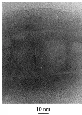
Fig. 6. High-resolution TEM image of CNFs grown on the Ni–P alloy catalyst at substrate temperature approximately 650 8C for 10 min.
Fig. 7. Field emission current density vs. electric field curves for CNFs. From curve (a) to (c), the thickness of Ni–P alloy catalyst
film corresponds to 20, 30 and 40 nm.Inset: Corresponding Fowler– Nordheim plot.
sheets. The peak which originates from finite size effects or lattice distortions located at approximately 1335ycm (D mode) is also observed, indicating the existence of
amorphous carbonaceous particles and defective graphite layers in the wall. The Raman spectra reveal that CNFs have a multiwalled structure with defective graphite sheets in the wall.
HRTEM was used to investigate and characterize the structure of CNFs. Fig. 6 is the HRTEM observation of the CNFs growth on sample B. The HRTEM image reveals that the CNFs are composed of parallel graphite planes tilted from their axis and have many defects in the tube wall. Sample A and sample C have the same structural characteristic as sample B. This result is consistent with the above observation of Raman spec-trum. The defects in the fiber wall cause the distortion of graphite plane and are reflected in the widening of the peak of the D mode.
3.4. Electron emission measurement
Fig. 7 illustrates the electron emission current density
vs. electric field (I–V) curves of CNFs. Curve (a) to
curve (c) in Fig. 7 give the I–V data from the CNFs
grown on sample A, sample Band sample C, respec-tively. For sample A, the turn-on field was approximately
0.11 Vymm with an emission current density of 10 mAy
cm and the threshold field was 3.1 V2 ymm with an
emission current density of 10 mAycm . Sample Band2
sample C have almost the same turn-on field
approxi-mately 0.22 Vymm, but the threshold field is 3.4 and
4.1 Vymm, respectively. These results show that all
CNFs exhibit outstanding emission properties including a low onset electrical field and high emission current densities. The inset in Fig. 7 shows Fowler–Norheim
(F–N) plots of the same emission data. The plot of
ln NIyVN vs. NIyVN is approximately a straight line,
indicating that the emitted electrons mainly follow the field emission process.
The field emission character of the CNFs is deter-mined by the intrinsic structure, chemical properties, aligned density and orientation of the nanofibers. How-ever, there is a lack of fundamental understanding of the mechanism responsible for the electron emission from carbon-based materials. The excellent field emis-sion properties of Ni–P alloy catalyzed-CNFs may be
attributed to the random orientation (as seen in Fig. 4)
and defects(as seen in Fig. 6) of CNFs. Davydov et al.
w24x have also pointed out that perfectly aligned CNTs
were less efficient field emitters and had lower field enhancement than chaotic CNTs. Meanwhile, Groning et al. w25x also suggested that some random CNTs exhibited better field emission properties than the aligned CNTs. These results keep confirming to our supposition. Another reason for the excellent field emis-sion properties is the defect effect. Some reports relating defect densities to field emission properties have also been proposed w26,27x. The enhanced emission may originate from the defect-induced energy bands that are formed within the band gap of graphite. The energy barrier that the electrons must tunnel through to be emitted is reduced, so the electrons residing at these defect levels can be emitted directly into vacuum from these bands or be transported to the surface states for emission w28x. Chen et al. w29x, in their research on field emission of different oriented CNTs, discovered that the CNTs oriented parallel to the substrate have a lower onset applied field than those oriented perpendicular to the substrate. They also suggested that the defect emis-sion mechanism is a reason for the low onset electrical field. Obraztsov et al. w30x have also found that the field emission properties were improved by increasing the density of structural defects.
Fig. 7 also indicates that the field emission properties of CNFs with small diameter are better than those of the CNFs with large diameter. Conventional field emis-sion analysis for carbon nanostructures utilizes the F–N equation, which can be written in terms of experimen-tally measured quantities as
2 3y2
Z
Z
ln IyV s BF
Ž
dyb yVqoffset..
where I is the total current, V is the applied voltage, d
is the distance between cathode and anode, b is the field enhancement factor, F is the emitter work function and B is equal to y6.83=109 (Vy(eV3y2m)). The
slopeS (i.e. BF dyb) of the F–N plot obtained from3y2
the experimental data is a constant and directly reflects
field emission properties. Here, d is an experimental
parameter,B is a constant, and only F and b are related
to the properties and structure of carbon nanostructures.
An in-depth study on F andB for CNTs was made by
Zhou et al. w31x. Their study revealed that F slightly increases and b gradually decreases with increasing tube diameter. The result completely supports our experimen-tal observation.
A clear fluctuation of theI–V curve at higher voltages
for CNFs is seen in Fig. 7, indicating some emission sites are damaged or destroyed. In particular, this phe-nomenon is obvious for CNFs with small diameter as in sample A. It is reasonable to suggest that the CNFs
with small diameter are more easily damaged by ion bombardment than the CNFs with large diameter w32x. 4. Conclusion
In this present study, an electroless nickel plating technique was used to deposit Ni–P alloy catalyst film for CNFs growth from methane in a microwave heating CVD system at 650 8C. The nanosized clusters on the clustered surface of Ni–P alloy catalyst film will directly provide the nucleation sites for CNFs without any pretreatment for catalyst film. The CNFs grown on Ni– P alloy catalyst shows random orientation for all samples with various thicknesses, but the diameter variation and the growth rate were clearly dependent on the initial thickness of catalyst film. Raman spectrum and HRTEM observations revealed that the multiwalled CNFs are composed of parallel graphite planes tilted from their axis and have many defects in the wall. Field emission measurements indicated that the CNFs with random orientation and many defects exhibited excellent field emission properties. The CNFs with small diameter has better field emission properties than the CNFs with large diameter, but were easily damaged by ion bombardment. Acknowledgments
The authors gratefully acknowledge research assis-tance by Wen-Jauh Chen and Shu-Hue Hsieh.
References
w1x A.M. Bonnot, M.N. Semeria, J.F. Boronat, T. Fournier, L.´ ´ Pontonnier, Diamond Relat. Mater. 9(2000) 852.
w2x V.I. Merkulov, D.H. Lowndes, Y.Y. Wei, G. Eres, E. Voelkl,
Appl. Phys. Lett. 76(2000) 3555.
w3x N.M. Rodriguez, J. Mater. Res. 8(1993) 3233.
w4x R.T.K. Baker, M.A. Barber, P.S. Harris, F.S. Feates, R.J. Waite,
J. Catal. 26(1972) 51.
w5x R.T.K. Baker, P.S. Harris, R.B. Thomas, R.J. Waite, J. Catal.
30(1973) 86.
w6x R.T.K. Baker, Carbon 27(1989) 315.
w7x M.S. Kin, N.M. Rodriguez, R.T.K. Baker, J. Catal. 131(1991)
60.
w8x Y. Li, J. Chen, L. Chang, Y. Qin, J. Catal. 178(1998) 76. w9x Z. Li, J. Chen, X. Zhang, Y. Li, K.K. Fung, Carbon 40(2002)
409.
w10x M. Ishioka, T. Okada, K. Matsubara, M. Endo, Carbon 30 (1992) 859.
w11x G.G. Tibbetts, Carbon 30(1992) 1399.
w12x T. Masuda, S.R. Mukai, K. Hashimoto, Carbon 30(1992) 124. w13x Y. Chen, S. Patel, Y. Ye, D.T. Shaw, L. Guo, Appl. Phys. Lett.
73(1998) 2119.
w14x K.B.K. Teo, M. Chhowalla, G.A.J. Amaratunga, et al., Appl.
Phys. Lett. 80(2002) 2011.
w15x M. Endo, Y.A. Kim, T. Hayashi, et al., Appl. Phys. Lett. 80 (2002) 1267.
w16x V.I. Merkulov, A.V. Melechko, M.A. Guillorn, D.H. Lowndes,
w17x Y.M. Shyu, F.C.N. Hong, Diamond Relat. Mater. 10 (2001)
1241.
w18x X.H. Chen, J.X. Wang, H.S. Yang, G.T. Wu, X.B. Zhang, W.Z.
Li, Diamond Relat. Mater. 10(2001) 2057.
w19x C.H. Ting, H. Paunovic, J. Electrochem. Soc. 136(1989) 456. w20x Y.Y. Wei, G. Eres, V.I. Merkulov, D.H. Lowndes, Appl. Phys.
Lett. 78(2001) 1394.
w21x M. Yudasaka, R. Kikuchi, T. Matsui, Y. Ohki, S. Yoshimura,
E. Ota, Appl. Phys. Lett. 67(1995) 2477.
w22x C. Bower, O. Zhou, W. Zhu, D.J. Werder, S. Jin, Appl. Phys.
Lett. 77(2000) 2767.
w23x Y.H. Mo, A.K.M.F. Kibria, K.S. Nahm, Synthetic Met. 122 (2001) 443.
w24x D.N. Davydov, P.A. Sattari, D. AlMawlawi, A. Osika, T.L.
Haslett, J. Appl. Phys. 86(1999) 3983.
w25x O. Groning, O.M. Kuttle, C. Emmenegger, P. Groning, L.
Shlapbach, J. Vac. Sci. Technol. B18(2000) 665.
w26x C. Wang, A. Garcia, D.C. Ingram, M. Lake, M.E. Kordesch,
Electron. Lett. 27(1991) 1459.
w27x N.S. Xu, R.V. Latham, Y. Tzeng, Electron. Lett. 29 (1993)
1596.
w28x W. Zhu, C. Bower, G.P. Kochanski, S. Jin, Solid-State Electron.
45(2001) 921.
w29x Y. Chen, D.T. Shaw, L. Guo, Appl. Phys. Lett. 76 (2000)
2469.
w30x A.N. Obraztsov, I.Y. Pavlovsky, A.P. Volkov, et al., Diamond
Relat. Mater. 8(1999) 814.
w31x G. Zhou, W. Duan, B. Gu, Appl. Phys. Lett. 79(2001) 836. w32x J.-M. Bonard, J.-P. Salvetat, T. Stockli, W.A. de Heer, L. Forro,¨ ´