國
立
交
通
大
學
電子工程學系 電子研究所碩士班
碩
士
論
文
金屬-氧化鈦鉿-金屬電容於動態記憶體與射頻電路
之應用
Metal-HfTiO-Metal Capacitors for DRAM/RF
Applications
研 究 生:徐曉萱
指導教授:崔秉鉞 博士
金屬-氧化鈦鉿-金屬電容於動態記憶體與射頻電路之應用
Metal-HfTiO-Metal Capacitors for DRAM/RF Applications
研 究 生:徐曉萱 Student:Hsiao-Hsuan Hsu
指導教授:崔秉鉞 博士 Advisor:Dr. Bing-Yue Tsui
國 立 交 通 大 學
電子工程學系 電子研究所碩士班
碩 士 論 文
A Thesis
Submitted to Department of Electronics Engineering and Institute of Electronics College of Electrical and Computer Engineering
National Chiao Tung University in Partial Fulfillment of the Requirements
for the Degree of Master in
Electronic Engineering July 2008
Hsinchu, Taiwan, Republic of China
金屬-氧化鈦鉿-金屬電容於動態記憶體與射頻電路之應用
研究生:徐曉萱 指導教授:崔秉鉞 博士
國立交通大學
電子工程學系 電子研究所碩士班
摘要
本篇論文中,我們採用高介電常數的二氧化鈦(TiO2),摻雜具有較大導帶不連續(conduction band offset)和能帶寬度的二氧化鉿(HfO2),混合而成的鈦化鉿
(HfTiO)材料作為金屬-氧化物-金屬(MIM)電容的介電質,來改善金氧金電容特 性,以達到動態記憶體以及射頻電路的需求。本論文重點在比較上電極的效應、 和介電層組成相關的漏電機制以及應力效應。在Pt/HfTiO/TaN 金氧金電容中, 我們得到一個高電容密度約 17.5 fF/µm2而所對應到的κ值為 37,且在電壓-1 伏特 下得到很低的漏電約 3.4x10⁻⁸ A/cm2。和Al電極相比,高功函數的Pt電極不只改 善漏電,同時可以改良類比特性,像是電壓電容係數(VCC)以及溫度電容係數 (TCC)。除此之外,不同的Hf含量對HfTiO介電層的特性改善亦有研究。實驗數 據顯示,增加Hf含量從 35%至 48%可以抑制漏電在電壓-3 伏特下約 1.5 個等級。 在改良漏電方面,我們成功發展出氮氣電漿處理HfTiO介電層上的方法,在電壓 -3 伏特下可以有效降低約兩個等級大小的漏電,同時維持電容密度以及VCC特 性。
為了找出降低VCC的方法,深入了解VCC的基本機制是必須的。由於影響 VCC特性的原因很多,在此,我們僅針對介電質的厚度效應、介電質成份組成以 及堆疊式金氧金結構(laminate MIM structure)三個方向來探討。實驗結果顯示增
加Hf的比例、增加介電層的厚度均可降低VCC。然而,使用HfTiO/Y2O3(三氧化 二釔)堆疊式電容亦可達到降低VCC的效果,這是由於Y2O3具有負的VCC-α可以 扺消具有正VCC-α的HfTiO,進而降低了VCC。 為了要達到高頻電容的需求,我們成功製造出厚度 51 奈米的HfTiO金氧金 電容,電容密度為 5.1 fF/µm2 ,且在電壓-1 伏特下的漏電為 1.3x10⁻⁹ A/cm2。此外, 在頻率 100 kHz下的VCC-α值約 40 ppm/V2 ,此一電容特性已符合 2012 ITRS的規 格。
最後,我們探討金氧金電容在定電壓應力測試(constant voltage stress)下,基 本電性以及電壓電容係數特性的變化。同時,可以觀察到電荷捕捉以及電荷釋放 的現象以及小於 1%的電容密度變化。使用 Pt 電極不僅可以降低漏電,同時可以 抑制應力產生漏電(stress-induced leakage current)和電容密度變化,並得到較好的 VCC 特性以確保長時間下的可靠度。
Metal- HfTiO -Metal Capacitors for DRAM/RF Applications
Student: Hsiao-Hsuan Hsu Advisor: Dr. Bing-Yue Tsui
Department of Electronics Engineering and Institute of Electronics
National Chiao Tung University
Abstract
In this thesis, we adopted a hafnium titanate (HfTiO) film as MIM dielectric, which dopes HfO2 with large conduction band offset and wide bandgap into high-κ
TiO2 (κ~50-80) to improve the performance of MIM capacitors for DRAM/RF
applications. The attention of the thesis is focused on the effect of electrodes, conduction mechanism, film composition, and stress behavior. Low leakage current of 3.4x10⁻⁸ A/cm2 at -1 V and high capacitance density of 17.5 fF/µm2, which reflects a
dielectric constant of 37, were obtained in a Pt/HfTiO/TaN MIM capacitor. Compared with Al top electrode, using high-work-function and thermodynamically stable Pt metal not only reduces the leakage current largely but also modify the analog characteristics (ex: VCC and TCC). Besides, the effect of Hf content on the performance of HfTiO dielectric was investigated. The experimental results indicate that the leakage current can be suppressed by nearly 1.5 orders of magnitude at gate bias of -3 V as Hf content increase from 35% to 48%. We developed successfully a N2
plasma treatment on HfTiO dielectrics to further lower leakage current by two orders of magnitude at -3 V and no apparent degradation is observed on the capacitance and VCC properties.
To find out the solutions for reducing voltage nonlinearity, thickness effect, film composition, and laminate MIM structure are investigated. From the experimental results, we found that the VCC properties can be reduced effectively as the increase of Hf content and thickness of HfTiO dielectrics. Similar effects also can be achieved by using a HfTiO/Y2O3 laminate, which adding Y2O3 results in a drop in VCC-α because
of canceling out the effect of positive VCC-α due to with the negative VCC-α of Y2O3. To meet the requirement of a RF capacitor, a 51 nm-thick Pt/HfTiO/TaN
capacitor was fabricated successfully, which a capacitance density of 5.1 fF/µm2 , low
leakage current of 1.3x10⁻⁹ A/cm2 at -1 V and very small VCC-α value of 40 ppm/V2
at 100 KHz were obtained to achieve the goals of 2012 ITRS.
Finally, we investigate the stress behavior of [Pt or Al]/HfTiO/TaN MIM capacitors on electrical properties and VCC characteristics under constant voltage stress (CVS). Charge trapping and trap generation phenomena are observed on the HfTiO MIM capacitors under CVS stress. Capacitance variation less than 1% can be achieved. The use of Pt electrode not only reduces the leakage current but also can suppress the stress-induced leakage current and capacitance variation to get a better VCC for long-term reliability.
謝誌
研究所兩年的生涯中,首先要感謝我的指導老師 崔秉鉞教授,老師的諄諄 教誨以及嚴謹認真的專業態度,總讓我受益匪淺;而老師的熱心公益以及耿直的 做人態度更是我學習的典範。 感謝實驗室的學長姐 李振銘、李振欽、洪玉仁、謝志民、盧季霈以及黃勻 珮在實驗上的討論幫忙與機台的訓練;感謝實驗室的夥伴 蔡雨蓁、張孝瑜、劉筱 函、張嘉文、羅正愷,有你們一起分享作實驗的酸甜苦辣,彼此加油打氣,真的 很棒;謝謝學弟們 周智超、蔡依成、羅子歆幫忙約 run 以及處理實驗室的事務, 讓我們可以更專心在實驗上,謝謝你們大家。謝謝曾俊元實驗室的學長以 林志 洋、吳明錡、林孟漢、同學 詹世緯的幫忙與建議,讓我在實驗上能很快的上手。 由衷感謝荊鳳德實驗室的學長 鄭淳護、黃靖謙以及鄧志剛,有了你們,讓我實 驗能夠一路披荊斬棘,越挫越勇。 謝謝我的好朋友們 陳玲、高珮玲、郭全雯、謝承佑以及游泳隊的夥伴們, 有你們六年來的的聊天與陪伴,美好的回憶我點滴在心,祝福你們。 最重要的感謝我親愛的父母 徐明芳先生、劉素淑女氏,謝謝你們從小的栽 培與照顧,以及姊姊 徐悅晴給予專業的諮詢,使我無後顧之憂得以完成論文。 我把這本論文獻給你們。Contents
Abstract (in Chinese)……….……….……….………i
Abstract (in English) ………..……….……….………….…iii
Acknowledgement……….……….……….………v
Contents……….……….………….……vi
Figure Captions……….……….……….…viii
Table Captions……….……….……….…xiii
Chapter 1 Introduction
1.1
Why Using HfO2 Doped TiO2 Dielectrics for MIM Capacitors……….……11.2
MIM Capacitors in RF Applications………..………..
….31.3
MIM Capacitors in DRAM Application………..41.4
The Organization of this Thesis………..……….……….6Chapter 2 Experimental Procedure
2.1
Device Fabrication………..…….……….…162.2
Material Analysis………...………...………172.3
Electrical Measurement………..……….………18Chapter 3 HfTiO MIM Capacitors for DRAM and RF Applications
3.1
Introduction………….………..………..…223.2
Basic Properties of the HfO2 Doped TiO2 Dielectrics……….…223.3
Leakage Current Improved by High-Work-Function Electrode…..……..………243.4
VCC Characteristics Improved by High-Work-Function Electrode………29Chapter 4 Improvement on Capacitance Behavior Dependence of
Voltage and Temperature
4.1
Introduction………..………...………..……554.2
The Physical Model of Voltage Nonlinearity………….………..………564.3
The Methods to Improve the Voltage Nonlinearity4.3.1
Effect of TiO2/HfO2 Ratio…………...…...………..……….……..584.3.2
Effect of Laminated Dielectric Structure..…..…………..……….……..614.3.3
Effect of Dielectric Thickness…..……….……..……….……..64Chapter 5 The Observation on Stress Performance of MIM
Capacitors under Constant Voltage Stress
5.1
Introduction………..………...………..……885.2
The Stress Behavior of Pt/HfTiO/TaN MIM capacitors………....885.3
The Stress Behavior of Al/HfTiO/TaN MIM capacitors……...………....91Chapter 6 Conclusions
6.1
Summary………..………...………..……1016.2
Future Works……….…………..………..………103References
……….………104Table Captions
Chapter 1 Introduction
Table 1-I
Summarized material and electric properties of several high-κ gate dielectrics………..…………..8Table 1-II
The requirement for RF devices according to ITRS……….……..9Table 1-III
DRAM stacked capacitor films technology requirements.….…….…10Table 1-IV
DRAM stacked capacitor potential solutions………..….…11Table 1-V
DRAM trench capacitor technology requirements…………..….…12Chapter 4 Improvement on Capacitance Behavior Dependence of
Voltage and Temperature
Table 4-I
The comparison of various high-κ MIM capacitors for the analog/RF applications. In this work, the Pt/HfTiO/TaN capacitor meets the requirements of ITRS at 2012.………..……..….…66Figure Captions
Chapter 1 Introduction
Fig. 1-1
Energy band alignment of various high-k dielectrics with respect to silicon. Dashed lines represent 1eV above and below the conduction and valence band, respectively, which point out the minimum barrier height to suppress the gate leakage current……….………13Fig. 1-2
Bandgap as the function of relative dielectric constant for various oxides Static dielectric constant versus band gap for candidate gate oxides….…14Fig. 1-3
The requirement of capacitance density for RF application versetechnology node in condition of the voltage linearity < 100 ppm/V2……15
Chapter 2 Experimental Procedure
Fig. 2-1
Fabrication flow of Pt/HfTiO/Y2O3/TaN/Ta MIM capacitor………….…19Chapter 3 HfTiO MIM Capacitors for DRAM and RF Applications
Fig. 3-1
(a) Auger depth profile of HfTiO/TaN with and without NH3 plasma onthe bottom electrode of TaN and (b) surface roughness of bottom electrode of TaN with and without NH3 plasma treatment by AFM
microscope……….…34
Fig. 3-2
(a) Cross-section TEM pattern of a 19 nm-thick HfTiO MIM capacitor,which gives the high-κ value of 37 and (b) the compositions of TaTiO interfacial layer by EDX analysis. (c) Cross-section TEM pattern of a 18 nm-thick Al/HfTiO/TaN MIM capacitor giving the high-κ value of 39…35
Fig 3-3
RBS spectra of the HfTiO dielectric. The ratio of HfO2:TiO2 is equal toFig 3-4
(a) C-V and (b) J-V characteristics of MIM capacitors using HfTiO or TiO2as a dielectric….……….………..…38
Fig 3-5
XRD patterns of TiO2 dielectric annealed at 400oC and HfTiO dielectricannealed at 400 and 600oC.….……….…….……..…39
Fig 3-6
Band diagram of a [Pt and Al]/HfTiO/TaN MIM capacitor.……….…..…40Fig 3-7
(a) C-V and (b) J-V characteristics of HfTiO MIM capacitors with Pt or Al top electrodes.….………..……….…….……..…41Fig 3-8
J-V characteristics of HfTiO MIM capacitors with top electrodes of (a) Pt and (b) Al under varied temperature from 25 to 125oC………...…42Fig 3-9
(a) Schottky emission fitting of v/HfTiO/TaN MIM capacitors at 25 and 125oC and (b) ohmic conduction fitting for Pt electrode at low electricfield at 25 oC………...……….…….……..…43
Fig 3-10
Schottky emission fitting of Al/HfTiO/TaN MIM capacitors at 25 and125oC….……….…….……..…44
Fig 3-11
ln (J/E)-E1/2 curve of Top electrode/HfTiO/TaN MIM capacitors at 25 and 125oC for (a) Pt and (b) Al electrodes…...….……..…45Fig 3-12
The Frenkel-Poole conduction fitting of HfTiO MIM capacitors for top (a) Pt electrode (b) Al electrode……….…….…….……..…46Fig 3-13
The VCC-α characteristics of (a) HfTiO and TiO2 MIM capacitors (b) [Ptor Al]/HfTiO/TaN MIM capacitors at 100 kHz and 1 MHz ….…...…47
Fig 3-14
VCC characteristics of Pt/HfTiO/TaN MIM capacitors under an elevated temperature range from 25oC to 125oC at (a) 100 kHz, (b) 1 MHz and the VCC-α as a function of temperature shown in (c)………48Fig 3-15
TCC characteristics of HfTiO MIM capacitors for (a) Pt and (b) Al top electrodes at different frequencies……….………50Fig 3-16
The (a) J-V, (b) C-V and (c) VCC-α characteristics of Pt/HfTiO/TaN MIM capacitors with or without N2 plasma treatment after post depositionannealing.……….…….……..…51
Fig 3-17
XPS depth profile for HfTiO dielectrics with and without N2 plasmatreatment on dielectric for (a) all elements within sputter time from 0 to 20 min and (b) only Ti, Hf snd N elements within sputter time from 0 to 6 min.……….…….……..…53
Fig 3-18
Surface roughness of HfTiO dielectrics with and without N2 plasmatreatment by AFM microscopy..……….…..…54
Chapter 4 Improvement on Capacitance Behavior Dependence of
Voltage and Temperature
Fig. 4-1
(a) C-V and (b) J-V characteristics of HfTiO dielectric for TiO2/HfO2ratio of 1.85 and 1.1………..….67
Fig. 4-2
(a) The TEM image of a capacitance density of 13 fF/µm2 HfTiOdielectric with 17 nm thickness which gives a high-κ value of 25, and (b) RBS spectra of the HfTiO dielectric. The ratio of HfO2:TiO2 is equal to
1:1.1, which is confirmed by ICP-MS.. ………..……..….68
Fig. 4-3
(a) J-V characteristics of HfTiO dielectric for TiO2/HfO2 ratio of 1.85 and1.1 at temperature range from 25 to 125oC and (b) the current density at -3 V for TiO2/HfO2 ratio of 1.85 and 1.1 at temperature range from 25 to
125oC………..………....….69
Fig. 4-4
(a) ln(J/T2)-E1/2 of Pt/HfTiO/TaN MIM capacitors with HfO2:TiO2=1:1.85
and 1:1.1 and (b) Ohmic conduction fitting for the ratio of 1:1.1 at low electric field………...….70
Fig. 4-5
VCC-α characteristics extracted at (a) 100 kHz and (b) 1 MHz for HfTiOMIM capacitor with the TiO2/HfO2 ratio of 1.85 and 1.1…...….71
Fig. 4-6
∆C/C0 as the function of voltage for TiO2/HfO2 ratio of 1.1 and VCC-αextracted at the frequencies of 100, 300, 500 kHz and 1 MHz at (a) 25oC and (b) 125oC and (c) VCC-α as a function of temperature measured at
different frequencies for TiO2/HfO2 ratio of 1.1...…73
Fig. 4-7
Trends of VCC-α values with respect to capacitance density when the ratio of HfO2 changes from 1.85 to 1.1...…74Fig. 4-8
The (a) C-V and (b) J-V characteristics of TiO2, HfO2 and Y2O3 MIMcapacitors...…75
Fig. 4-9
The VCC-α characteristics of (a) TiO2 (b) HfO2 (c) Y2O3 MIM capacitorsat different frequencies. ...…76
Fig. 4-10
The (a) VCC-α characteristics at 100 kHz and (b) frequency dependenceof VCC-α for TiO2, HfO2 and Y2O3 MIM capacitors…...…78
Fig. 4-11
The TCC characteristics of a Pt/Y2O3/TaNMIM capacitor at thefrequencies of 100 kHz, 300 kHz and 500 kHz…...…79
Fig. 4-12
XRD analysis of Y2O3 dielectric under 400oC and 600oC PDA...…80Fig. 4-13
The TEM images of (a) a HfTiO (~12 nm)/Y2O3 (~5 nm) laminated MIMcapacitor and (b) a 15 nm-thick HfTiO MIM capacitors, respectively..…81
Fig. 4-14
The C-V and J-V characteristics of HfTiO MIM capacitors with or without Y2O3 layer...…82Fig. 4-15
The (a) VCC characteristics at 100 kHz and (b) frequency depdence of VCC-α for HfTiO/Y2O3 laminated MIM capacitors...…83Fig. 4-16
(a) C-V and (b) J-V characteristics of a 51 nm-thick HfTiO MIM capacitor...84Fig. 4-17
The VCC-α characteristics of Pt/HfTiO/TaN MIM capacitors at thefrequencies of 100, 300 and 500 kHz. ...85
Fig. 4-18
S E M i m a g e o f a P t / H f Ti O / Ta N M I M c a p a c i t o r w i t h a51nm-thickness…...86
Fig. 4-19
VCC-α verse 1/C plot for various high-κ MIM capacitors. The exponential decrease with increasing 1/C is important to design capacitors for different applications……..…...87Chapter 5 The Observation on Stress Performance of MIM
Capacitors under Constant Voltage Stress
under different negative bias by constant voltage stress…………..…..93
Fig. 5-2
The effect of constant-voltage stress biased at -3.5 V on (a) C-V and (b)J-V of Pt/HfTiO/TaN capacitors…….………..………...…..94
Fig. 5-3
The effect of constant-voltage stress biased at -5 V on (a) C-V and (b) J-V of Pt/HfTiO/TaN capacitors…….………..………...…..95Fig. 5-4 (
a) C-V and (b) J-V of Pt/HfTiO/TaN capacitors before stress or afterdifferent stress condition………….………..………...…..96
Fig. 5-5
Charge-induced capacitance variation (a) measured at regular intervals of 1000 sec after CVS and (b) as a function of stress time at different biased voltage by CVS………..………….………..………...…..97Fig. 5-6
Leakage current-stress time properties of Al/HfTiO/TaN capacitors under CVS biased at -2.5 V and -3 V……….……….…………...…..98Fig. 5-7
The effect of constant-voltage stress biased at -2.5 V and -3 V on (a) C-V and (b) J-V of Al/HfTiO/TaN capacitors……….………...…..99Fig. 5-8
Charge-induced capacitance variation under different biased voltage byChapter 1
Introduction
1.1 Why Using HfO
2Doped TiO
2Dielectrics for MIM Capacitors
In recent years, a global research has been implemented to identify suitable high-dielectric-constant (high-κ) materials. In CMOS technology, the continuous downscaling of the gate dielectric thickness to achieve further gains in performance and productivity is an enormous task due to direct tunneling currents and boron penetration in SiO2 below 1.5 nm. Similar problems are expected in the case of the
dynamic random access memory (DRAM) storage capacitor dielectrics. According to International Technology Roadmap for Semiconductors (ITRS) [1.1], migration of gigabit DRAM capacitor structures from silicon-insulator-metal (MIS) to metal-insulator-metal (MIM) with design rules of 0.10 µm and below is essential [1.2]. In addition, MIM capacitors in silicon analog circuit applications have attracted great attention due to their high conductive electrodes and low parasitic capacitance between the capacitor and the substrate [1.3, 1.4].
The accelerative downscaling of metal-insulator-metal (MIM) capacitors requires a corresponding reduction in the thickness of dielectrics to achieve high capacitance density and thus results in increasing leakage current and poor voltage linearity [1.5]. In addition to the leakage issue, as an increase in the integration level and the scale-down of chip size, capacitors consume a large fraction of the area and thus disputing reduction of the circuit density and the system cost. From the viewpoint of power consumption, capacitance density, and circuit density, one solution for these problems is to replace conventional silicon dioxide [1.6] and silicon nitride [1.3, 1.5, 1.7]with high-κ dielectrics to maintain the capacitance density in each generation as
well as suppress the leakage current. Table 1-I illustrates the summarized material and electric properties of several high-κ gate dielectrics [1.8]. High-κ dielectrics have been proposed for several years, such as HfO2 [1.9–1.12], Al2O3 [1.12, 1.15],
(HfO2)1-x(Al2O3)x [1.13], AlTaO [1.14], AlTiOx [1.15], and Ta2O5 [1.12, 1.16], for
MIM capacitors.
Among these investigated high-κ dielectrics, titanium oxide, TiO2 dielectrics
have been characterized by its high dielectric constant (κ~50-80) [1.17], which makes it’s potentially useful in various roles in integrated circuits (IC), including capacitors, gate oxides, and other circuit elements [1.18, 1.19]. It is believed that dielectric constant variability is related to the presence of low-permittivity interfacial layers and to the difference crystalline phase. The dielectric constant of TiO2 changes from ~31
to 60-100 for crystalline anatase and rutile, respectively [1.20, 1.21]. Although TiO2
has a merit of high dielectric constant, the small band offset is a serious concern on the leakage current due to the limitation for real devices. Therefore, a critical goal is to increase the breakdown field and reduce the leakage current density.
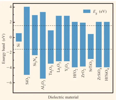
Fig.1-1 shows the energy band alignment of various high-κ dielectrics with respect to silicon. The dashed lines represent 1 eV above and below the conduction and valence band, respectively, which point out the minimum barrier height to suppress the leakage current [1.22]. One approach to decrease leakage current due to eliminate defects in TiOx might be the incorporation of foreign cations into the thin
film. It has also been reported that adding 10-30 at.% of Nd, Tb, or Dy to amorphous Ti–O thin films can decrease the leakage current, increase the breakdown voltage, and yet retain the relatively high dielectric constant (k~50-100) [1.23]. In addition, Zirconium titantate-based thin films have been determined to be the promising candidate for ultra-large-scale integration [1.24]. The element of Sn can further improve the electrical properties of amorphous Ti–Zr oxide [1.25]. As shown in Fig.
1-2, the trend of bandgap decline with increasing relative dielectric constant [1.8]. There is a trade-off between the leakage current and the dielectric constant. Therefore, the merit of introducing HfO2 is its medium dielectric constant (k~20) and large band
offset (ΔEc~1.5 eV) which might compensate the leakage issue of TiO2 dielectrics
and maintain high dielectric constant at the same time. In addition, from the viewpoint of high-κ dielectrics materials, low-valence ions in TiO2 will produce oxygen
vacancies, which lead to a higher ionic conductivity. For example, 8% Y2O3 (Y3+)
doped HfO2 results in a high ionic conductivity of 0.03 Ω-1cm-1 is reported due to
low-valence ions doping [1.26]. Ti and Hf are both four-valence elements. So HfO2
doped TiO2 would not exhibit any increase in oxygen voids which attribute the
leakage current in the film.
Many articles [1.27-1.31] studied the electrical as well as structural properties of mixtures of HfO2 and TiO2 as possible high-κ gate dielectrics. However, relatively
few attempt to investigate the mixture of HfO2 and TiO2 as the dielectrics in the MIM
capacitors.
1.2 MIM Capacitors in RF Applications
The dramatic increase in wired and wireless communications in recent years has demanded the need for high quality passives for mixed and analog signal applications. MIM capacitors, which are typically used in RF circuits for impendence matching and direct current (DC) filtering, as well as analog capacitors in mixed-signal product [1.5], draw much attention due to its high quality factor low parasitic capacitance better matching, and small voltage coefficient of capacitance (VCC) [1.6, 1.32],
Both in analog and RF applications, one of the desired properties of MIM capacitors is a high degree of voltage linearity also called voltage coefficient of capacitor (VCC), which traduces the dependence of capacitance on the applied bias.
In MIM capacitors, one of the greatest challenges is to achieve small VCC, which is required for capacitors to minimize harmonic generation and improve balancing [1.33, 1.34]. According to International Technology Roadmap for Semiconductor (ITRS), VCC is required less than 100 ppm/V2 from now on to 2020 as showed in Table 1-II and Fig. 1-3 [1.1].
Except the specification for VCC, the dielectrics of MIM capacitors has to fulfill the following main requirement: (1) high capacitance density (>5 fF/µm2), in
terms of ITRS, the need for RF capacitor is 4 to 12 fF/µm2 in 2008 to 2020, (2) low leakage currents (10−8 A/cm2), (3) high breakdown electric field (holding at least a voltage bias of 5 V), and (4) low dielectric loss [tanδ<0.05, i.e., Q factor (=1/ tan δ)>20] [1.35]. Moreover, a low thermal budget (450℃) is required for MIM capacitors to be compatible with Cu back-end-of-line (BEOL) process, since the devices are located in the interconnection levels and above the active integrated circuit layers.
1.3 MIM Capacitors in DRAM Applications
Today, most of computer memory chips use the dynamic random access memory (DRAM) in which each bit of information is stored in a memory cell consisting of one transistor and one capacitor (1T1C). This kind of memory was first invented by an IBM researcher named Robert Heath Dennard in 1967. It has become a breakthrough that made DRAM become the standard memory chip for personal computers replacing magnetic core memory. Until 1972, Intel had already released the world's first generally available 4 Kb DRAM chip and transformed the microelectronics industry throughout. Nowadays, DRAMs have been advanced by focusing on how to make memory cells smaller to realize higher density DRAMs.
challenges, especially in the cell capacitance point of view. Memory cell capacitance is the key parameter which determines the sensing signal voltage, sensing speed, data retention times and endurance against the soft error event [1.36]. In the Gbit era, it’s generally accepted that the minimum cell capacitance should be kept more than 25 fF regardless of density. The strategies for achieving higher cell capacitance are either reducing the thickness of the dielectrics or adopting high-κ materials. However, aggressive scaling down the thickness would result in leakage current, power consumption, and reliability issues due to electrons tunneling [1.37]. In order to offer the thicker physical thickness and maintain the same capacitance density, high-κ capacitor becomes the only one solution [1.38].
For DRAM trench capacitor, using of NO dielectric (nitride/oxide stack) has been extended through the 70 nm generation, with high-κ materials being introduced at the 65 nm generation [1.1]. According to the ITRS, dielectric constant of 50 is demanded for the stacked DRAM from now on to the year of 2010 as shown in Table 1-III [1.1]. Table 1-IV [1.1] shows the possible materials for DRAM stacked capacitor although mass-production solutions are not optimized yet after 2010 [1.1, 1.39]. Table 1-V also presents the requirements for the DRAM trench capacitor [1.1].
In the recent years, thin film perovskite materials with ultra high-κ such as PZT [1.39], SrTiO3 [1.40] and (Ba,Sr)TiO3 [1.41] have been investigated as dielectric
materials for DRAM. According to 2007 ITRS roadmap [1.1], one of the difficult challenges is scaling of the physical dielectric thickness, Tphy while maintaining
dielectric constant and leakage current of dielectrics. To obtain ultra high-κ value (κ > 130) for DRAM requirement of 2014 ITRS, large leakage current caused by small conduction band offset (~ -0.1 eV) will be unacceptable for SrTiO3 materials.
Therefore, thicker thickness is required to reduce the electric field across the dielectric. However, these ultra high-κ dielectrics have the thickness limit due to the capacitor
geometry, since the aspect ratio of the deep trench and metal-1 contact of stacked capacitors [1.42], which are related to the ability of gap-filling, should be taken into consideration. In particular, the G-bit DRAM will only have space for a dielectric layer no thicker than 20 nm [1.43]. Besides, it’s a challenge to deposit ternary materials into high aspect ratio structures with a uniform film composition by CVD process, let along PVD process. Also, these ultra high-κ dielectrics aren’t suitable for RF applications due to low thermal budget issues and much lower capacitance density being needed. Therefore, around 10 nm thin film and high-κ dielectric of HfTiOx is
adopted in this thesis to achieve parts of the specifications for both RF and DRAM applications.
In addition to the high dielectric constant, low leakage current is another key design feature for DRAM cells, since the refresh interval is governed by the stored charge loss at the capacitor [1.44, 1.45]. Increasing tunneling current due to scaling down the dielectrics has been shown in D. J. Frank et al.[1.46]. In terms of the ITRS
shown in Table1-III, leakage current around 1x10⁻⁷ A/cm2 is acceptable until 2020.
1.4 The Organization of this Thesis
The organization of this thesis is briefly described below. Chapter 1 depicts the motivation to adopt the high-κ HfTiO dielectrics and the MIM capacitors in RF and DRAM applications. Chapter 2 describes the process procedure of the HfTiO MIM capacitors as well as the methods of electrical and material analysis. Chapter 3 discusses the electrical characteristics of HfTiO MIM capacitor using in RF and DRAM field. The effects of top electrode and plasma treatment have also been investigated. Chapter 4 illustrates the physical model of charge trapping and detrapping to explain the mechanism of voltage nonlinearity. Four methods to improve the voltage linearity is also proposed, including using high work function top
electrode, increasing the amount of HfO2, adopting stack structure and increasing the
dielectric thickness. Chapter 5 studies the long-term reliability of HfTiO MIM capacitors with top electrodes of Pt and Al in terms of constant voltage stress (CVS). Chapter 6 summarizes the conclusions and contributions of this thesis, and provides the suggested directions for further research.
Table 1-I Summarized material and electric properties of several high-κ gate dielectrics [1.8].
Dielectric Dielectric constant Bandgap (eV) Conduction band offset Thermal stability on Si substrate SiO2 3.9 9 3.5 >1050℃ Si3N4 7 5.3 2.4 >1050℃ Al2O3 ~10 8.8 2.8 ~1000℃ Ta2O5 25 4.4 0.36 Not stable La2O3 ~21 6* 2.3 Gd2O3 ~12 Y2O3 ~15 6 2.3 Silicate formation HfO2 ~20 6 1.5 ~950℃ ZrO2 ~23 5.8 1.4 ~900℃ SrTiO3 3.3 ~0.1 ZrSiO4 6* 1.5 HfSiO4 6* 1.5 *Estimated value
Table 1-II The requirement for RF devices according to ITRS [1.1]. Metal-Insulator-Metal Capacitor Year of Production 2008 2010 2012 2014 2016 2018 2020 Density (fF/µm2) 4 5 5 7 10 10 12 Voltage linearity (ppm/V²) <100 < 100 < 100 < 100 < 100 < 100 < 100 Leakage (A/cm²) <1e-8 <1e-8 <1e-8 <1e-8 <1e-8 <1e-8 <1e-8
σ Matching
(%·µm) 0.5 0.4 0.4 0.3 0.2 0.2 0.2
Table 1-III DRAM stacked capacitor films technology requirements [1.1]. Year of Production 2008 2010 2012 2014 2016 2018 2020 DRAM ½ Pitch (nm) 57 45 36 28 22 18 14 Capacitor structure Cylinder / Pedestal MIM Cylinder / Pedestal MIM Cylinder / Pedestal MIM Pedestal MIM Pedestal MIM Pedestal MIM Pedestal MIM teq at 25fF (nm) 0.90 0.60 0.40 0.30 0.30 0.30 0.20 Dielectric constant 43 65 98 130 91 78 80
Leak current (fA/cell) 0.70 0.64 0.64 0.59 0.41 0.35 0.35
Leak current density
(nA/cm2) 107.9 148.4 222.6 269.8 188.8 161.9 242.8 Vcapacitor (Volts) 1.2 1.1 1.1 1 0.7 0.6 0.6 Retention time (ms) 64 64 64 64 64 64 64 Deposition temperature (degree C) ~500 ~500 ~500 ~500 ~500 ~500 ~500 Film anneal temperature (degree C) ~750 <750 ~650 <650 <650 <650 <650
Table 1-IV DRAM stacked capacitor potential solutions [1.1, 1.43].
Year of Production 2008 2010 2012 2014 2016 2018 2020
DRAM M1 1/2-pitch (nm) 65 45 45 32 22 16 16
DRAM Product 4G 4G 8G 16G 32G 32G 32G
Top Electrode TiN Ru, RuO2, Pt, IrO2, SrRuO…..
Dielectric Material HfO2, Ta2O5, ZrO2 TiO2, STO, BST
Bottom Electrode TiN Ru, RuO2, Pt, IrO2, SrRuO…..
Table 1-V DRAM trench capacitor technology requirements [1.1].
Year of Production 2008 2010 2012 2014 2016
DRAM ½ Pitch
(nm) 57 45 36 28 22
Trench structure bottled bottled bottled bottled bottled
Trench circumference (nm) 483 374 300 233 208 Effective oxide thickness (CET)(nm) 2.8 1.8 1.1 0.7 0.6 Cell size (µm2) 0.028 0.016 0.0104 0.0063 0.0039 Trench depth [µm], (at 35fF) 6 5.6 4.5 3.7 3 Aspect ratio 74 89 89 94 97 MIS/High-κ Capacitor
Fig. 1-1 Energy band alignment of various high-κ dielectrics with respect to silicon. Dashed lines represent 1 eV above and below the conduction and valence band, respectively, which point out the minimum barrier height to suppress the gate leakage current [1.22].
0
10
20
30
40
50
60
0
2
4
6
8
10
Bandgap (eV)
Relative dielectric constant
SiO2 Al2O3 La2O3 Y2O3 HfO2 ZrO2 Si3N4 Ta2O5 Pr2O3 TiO2 CeO2Fig. 1-2 Bandgap as the function of relative dielectric constant for various oxides [1.26].
0 2 4 6 8 10 12 14
ITRS 2007 for RF Capacitors
Solutions are optimized Solutions are known
Solutions are NOT known
45 32 22 19 65 Technology Node (nm) Ca paci tance Densit y (fF/ µ m 2 ) Voltage linearity <100 ppm/V2
Fig. 1-3 The requirement of capacitance density for RF application verse technology node in condition of the voltage linearity < 100 ppm/V2 [1.1].
Chapter 2
Experimental Procedure
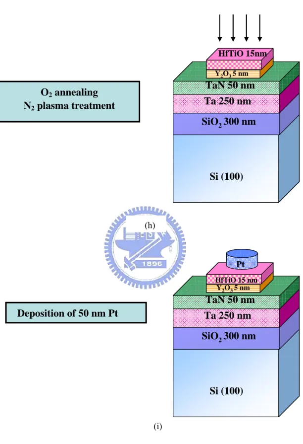
2.1 Device Fabrication
Four inches diameter n-type (100) silicon wafers with a nominal resistivity of 10 to 100 Ω-cm were used as substrates. Wafers were cleaned by the standard RCA clean process to remove particles and metal ions and followed by a 300 nm thick SiO2
growth by wet oxidation at 950 for 1 hour℃ to ensure the substrate isolation. Then Ta(50 nm)/TaN(250 nm) bottom electrode was deposited without breaking vacuum by DC sputtering of Ta target and was patterned by the shadow mask as shown in Fig 2-1 (a)-(d). The chamber pressure during the deposition was maintained at 6 mtorr with an Ar flow rate of 30 sccm and Ar/O2 flow rate of 30/1.8 sccm for Ta and TaN,
respectively. Neither substrate bias nor substrate heating was intentionally applied. Ta was used to reduce series resistance and TaN acts as the diffusion barrier [2.1, 2.2] between the high-κ HfTiO and the Ta/TaN electrode.
After bottom electrode deposition, NH3 plasma treatment was introduced by
multi-chamber plasma enhanced chemical vapor deposition (multi-PECVD) with power of 200 W and NH3 flow rate of 700 sccm for 15 min to suppress the growth of
interfacial layer [2.1]-[2.5] as shown in Fig 2-1 (e). During plasma treatment, the chamber pressure was 600 torr and the substrate was kept at 300 ℃.
Before depositing of HfTiO dielectrics, Y2O3 film was deposited on some
samples as shown in Fig 2-1 (f). The Y2O3 film was formed by dual E-gun
evaporation using Y2O3 slits. The chamber pressure is kept at 5x10⁻² torr and without
substrate heating intentionally. The thicknesses of Y2O3 films were in the range of 5 to
Then HfTiO films were formed as depicted in Fig. 2-1 (g) via dual E-gun evaporation using the source of TiO2 and HfO2 slits at a substrate temperature of 25
℃. The chamber pressure was maintained at 5×10⁻² torr. The thicknesses of HfTiO films were in the range of 10 to 40 nm and were controlled by quartz crystal oscillation. The actual thicknesses were precisely measured by transmission electron microscopy (TEM) or scanning electron microscopy (SEM).
After the preparation of HfTiO dielectrics, all of the wafers were annealed at 400℃ in O2 ambient furnace for 10 to 90 min to eliminate defects and assist in fully
oxidation. The selection of annealing time depends on the film thickness. It’s noted that annealing temperature was kept at 400℃ for MIM capacitor fabrication to meet the thermal budget requirement of Cu back-end-of-line (BEOL) process. After formation of HfTiO dielectrics and annealing process, some samples were introduced N2 plasma treatment to further improve electrical performance as shown in Fig. 2-1
(h). The N2 plasma treatment was carried on by a multi-chamber plasma enhanced
chemical vapor deposition (multi-PECVD) system with power in the range of 10 to 100 W and N2 flow rate of 500 sccm for 20 sec to 300 sec. During the N2 plasma
treatment, the chamber pressure was 600 torr and substrate was kept at 300℃.
Finally, the counterparts of MIM capacitors with Pt and Al metals as top electrodes were fabricated for comparison purpose. Pt electrode was deposited by dual E-gun evaporation using Pt slits as shown in Fig. 2-1 (i) and Al electrode was deposited by thermal evaporation. The top electrode of MIM capacitors were patterned by shadow mask with area of 3.14×104 µm2 in circle.
2.2 Material Analysis
The surface roughness was measured by atomic force microscopy (AFM) working in contact mode. The scan rate was 1 Hz. The root mean square (rms)
roughness values were calculated on a 5×5µm2 area. The Hf:Ti ratio was detected by
Rutherford backscattering spectroscopy (RBS) with 2 MeV He2+ ions and was double checked by inductively coupled plasma-mass spectrometer (ICP-MS). The resulting spectra were analyzed by integration methods. X-ray diffraction (XRD) was employed to identify the crystal structure of the films using Cu Kα radiation withλ =0.5418 nm. Film morphology and interfacial details were investigated by transmission electron microscope (TEM). Auger electron spectroscopy (AES) was used to determine atomic depth profile and inter-diffusion between films. AES depth profiles of the samples were carried on using Ar+ sputtering. After removing top electrodes, chemical bonds in the HfTiO dielectrics and the interfacial layer between HfTiO dielectric and bottom electrode were examined by X-ray photoelectron spectroscopy (XPS).
2.3 Electrical Measurement
For electrical measurement, the leakage current-voltage (J-V) curves were measured by the semiconductor parameter analyzer of model Agilent 4156C. The capacitance-voltage (C-V) curves were measured by the precision impedance meter of model Agilent 4284A at frequencies varied from 100 kHz to 1 MHz by applying a small ac (25 mV) signal. To analyze the reliability of the dielectrics, constant voltage stress (CVS) was also conducted. In order to investigate the thermal stability of the high-κ dielectric film, thermal stress was carried on with measurement temperatures varied from 25 to 125℃. For all of the electrical measurement, the voltage is biased to the top electrode, while the bottom electrode is grounded.
RCA cleaned Si wafer
Si (100)
(a)
SiO
2300 nm
Si (100)
Wet oxidation 300 nm SiO
2(b)
SiO
2300 nm
Ta 250 nm
Si (100)
Sputtering 250 nm Ta
(c) (d)SiO
2300 nm
Ta 250 nm
TaN 50 nm
Si (100)
Sputtering 50 nm TaN
Si (100)
SiO
2300 nm
Ta 250 nm
TaN 50 nm
HfTiO 15nm Y2O3 5 nmSi (100)
SiO
2300 nm
Ta 250 nm
TaN 50 nm
HfTiO 15nm Y2O3 5 nmSi (100)
SiO
2300 nm
Ta 250 nm
TaN 50 nm
NH
3plasma treatment
(e)SiO
2300nm
Ta 250 nm
TaN 50 nm
Y
2O
35 nm
Si (100)
Deposition of 5 nm Y
2O
3 (f)Deposition of 15 nm HfTiO
(g)Si (100)
SiO
2300 nm
Ta 250 nm
TaN 50 nm
Y2O3 5 nm HfTiO 15nmSi (100)
SiO
2300 nm
Ta 250 nm
TaN 50 nm
Si (100)
SiO
2300 nm
Ta 250 nm
TaN 50 nm
Si (100)
SiO
2300 nm
Ta 250 nm
TaN 50 nm
Y2O3 5 nm HfTiO 15nmO
2annealing
N
2plasma treatment
(h)Si (100)
SiO
2300 nm
Ta 250 nm
TaN 50 nm
Y2O3 5 nm HfTiO 15 nm PtSi (100)
SiO
2300 nm
Ta 250 nm
TaN 50 nm
Si (100)
SiO
2300 nm
Ta 250 nm
TaN 50 nm
Si (100)
SiO
2300 nm
Ta 250 nm
TaN 50 nm
Y2O3 5 nm HfTiO 15 nm PtDeposition of 50 nm Pt
(i)Chapter 3
HfTiO MIM Capacitors for DRAM and RF Applications
3.1 Introduction
Dielectric materials for MIM capacitors with high dielectric constant (κ~ 20-40) have to be surveyed and researched for stacked and trench capacitors before 2010. Besides, the physical thickness of high-κ dielectric also should be scaled down to fit the minimum feature size. On trench DRAM technology, a thicker dielectric would increase the difficulty in film filling process caused by more and more large aspect ratio. On the other hand, the medium dielectric constant materials (5<κ<40) or laminated stack structure would be good solutions for RF application.
In this chapter we propose a mixed high-κ dielectric (κ∼ 35−38) for DRAM/RF applications and discuss the improvement on the capacitors properties by different top electrodes and plasma treatment.
3.2 Basic Properties of the HfO
2Doped TiO
2Dielectrics
Fig. 3-1 (a) shows the Auger depth profile of HfTiO/TaN with and without NH3
plasma treatment on the bottom electrode of TaN. The titanium metal penetration into bottom electrode can be observed in the samples without NH3 plasma treatment. It
implies that the thicker interfacial layer of TiTaO is formed at the bottom interface during PDA process. It may result in the degradation of the overall performance. In contrast, the samples with NH3 plasma on bottom electrode exhibit less metal interdiffusion. This can
suppress the formation of bottom interface layer. From the bottom surface morphology analyzed by AFM spectroscopy shown in Fig. 3-1 (b), root mean square (rms) roughness of 0.35 nm and 0.57 nm were observed on the samples with or without plasma treatment, respectively. It is believed that increased surface roughness can be interpreted as an image force that lowers the barrier height for electron injection [3.1, 3.2]. Therefore, in this thesis, the bottom electrode of all MIM samples will be treated by NH3 plasma.
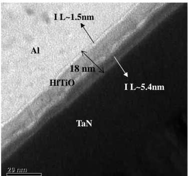
Fig. 3-2 (a) shows the cross-sectional TEM image of the Pt/HfTiO/TaN MIM capacitor with a capacitance density of 17.6 fF/µm2
. A 19 nm-thick HfTiO dielectric with a 4.8 nm-thick bottom interfacial layer which gives a κ value of 37 was observed. In Fig. 3-2 (b), the EDX analysis shows the compositions of interfacial layer marked in TEM picture is TiTaO. In this thesis, we only investigated the electrical properties of MIM capacitors such as leakage current mechanisms and analog properties like VCC and TCC under negative bias but those under positive bias are not discussed to avoid the disturbance due to this bottom interfacial layer. From Fig. 3-2 (c), cross-sectional TEM pattern of the Al/HfTiO/TaN MIM capacitor shows a 18 nm-thick HfTiO dielectric with 1.5 and 5.4 nm-thick interfacial layers at the top and bottom electrodes, respectively, which gives a κ value of 39.
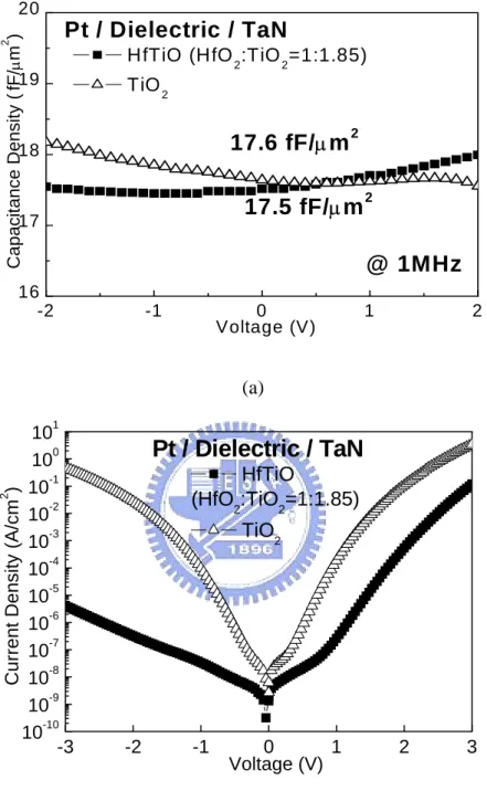
ICP-MS analysis identified that the ratio of TiO2/HfO2 is equal to 1.85 which is
confirmed by the RBS spectra in Fig. 3-3. Fig. 3-4 (a) and (b) show that the leakage current of HfTiO dielectric is lower than TiO2 dielectrics by almost five orders of
magnitude at -3 V at the similar capacitance density of ~17.5 fF/µm2
. In addition, the oxidation of bottom TaN electrode and a poor interface formation after 400oC-PDA will result in a larger electron tunneling current from bottom electrode than that from top electrode. From the asymmetry C-V curve, the more apparent voltage dispersion at
positive bias may be caused by the poor interface between bottom electrode and dielectric.
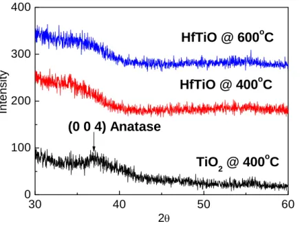
The structural properties of TiO2 and HfTiO dielectrics experienced different PDA
temperatures were investigated by x-ray diffraction (XRD) and the spectra are shown in Fig. 3-5. Significant (004) diffraction peak of crystallized-TiO2 with an anatase phase is
observed in the TiO2 dielectric after 400oC annealing in O2 atmosphere for 10 min. The
large leakage current due to low electron barrier height and crystallization of the TiO2 at
low temperature is a major limitation for device applications. In contrast, the HfTiO dielectric remains amorphous even after 600oC-PDA in O2 atmosphere for 10 min.
Importantly the spectrum of HfTiO dielectric shows no evidence of TiO2 with rutile or
anatase phase, even though the film was a titanium-rich metal oxide (HfO2:TiO2=1:1.85).
It has been known that HfO2 is crystallized after 600oC-PDA [3.3]. Our results suggest
that the crystallization phenomenon can be suppressed by the combination of the HfO2
and TiO2 up to 600oC-PDA at least.
3.3 Leakage Current Improved by High-Work-Function Electrode
Fig. 3-6 shows the energy band diagram of the [Pt and Al]/HfTiO/TaN MIM capacitor. The electron affinity of HfTiO dielectric is assumed to be between 2.5~3.9 eV, which corresponds to that of HfO2 and TiO2 are 2.5 and 3.9 eV [3.4], respectively, and is
nearly 2.55~4.15 eV reported by K. C. Chiang et al. [3.5]. Since electron affinity of Ta2O5
is 3.2 eV [3.4], the electron affinity of interfacial layer of TaTiO was considered to be approximately 3.4~3.9 eV [3.6] and then the variation of the electron affinity is dependent on film compositions. High work function top electrode such as Pt is expected to achieve low leakage current.
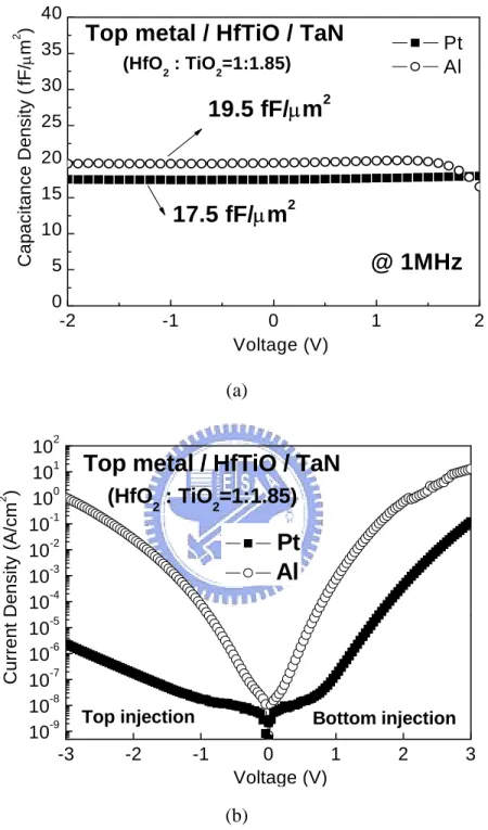
The capacitance densities for Pt and Al top electrodes are 17.5 fF/µm2
and 19.5 fF/µm2
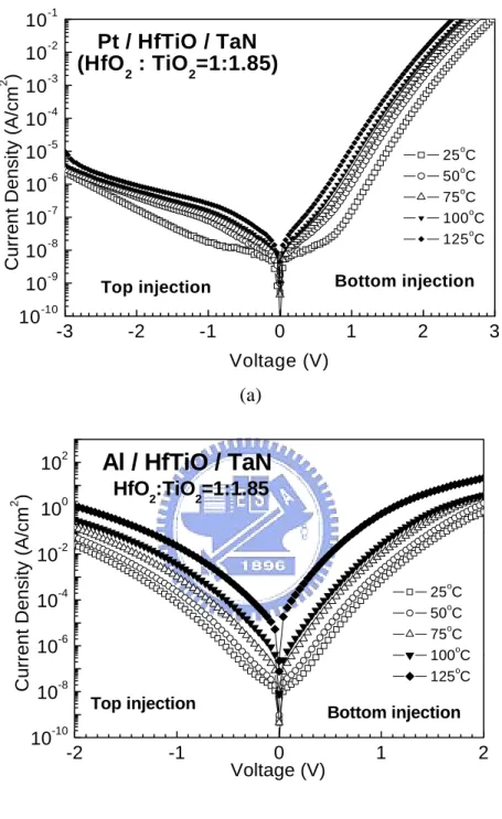
, respectively, calculated from the 1 MHz C-V characteristics shown in Fig. 3-7 (a). The capacitance densities are almost constant with varied bias from -2 to 2 V for Pt top electrode, but larger voltage dispersion for Al top electrode beyond +1.5 V bias is due to larger leakage current. The top electrode area is 3.14×104 µm2 in circlefor all of the capacitors. The difference of capacitance density for HfTiO MIM capacitors with Pt or Al top electrodes may be caused by different metal deposition process or film uniformity. From the J-V characteristics in Fig. 3-7 (b), the leakage current density for Pt electrode measured at -1 V at room temperature is much lower than that for Al electrode by three orders of magnitude although the capacitance density of Pt electrode is slightly lower than that of Al electrode.
The gate injected leakage currents for both Pt and Al case are contributed from not only high density of traps in dielectric caused by incomplete dielectric activation but also the different Schottky barrier heights between top electrode and dielectric. This may be due to larger work function difference between top Pt and bottom TaN electrodes increasing metal-insulator barrier height to suppress the leakage current from top or bottom carrier injection. Beside this, several phenomena such as Fermi level pinning or the formation of interfacial layer between top metal and insulator as shown in Fig. 3-2 (c) may also affect the leakage current. Therefore, current transport mechanisms should be investigated carefully.
The J-V characteristics of the MIM capacitor with Pt and Al as top electrodes measured at temperatures ranging from 25 to 125oC are shown in Fig. 3-8 (a) and (b), respectively. A small leakage current and weak temperature dependence of 2.4x10⁻⁶ and 9.8 x10⁻⁶ A/cm2 at 25 and 125oC for Pt electrode are obtained, respectively, at -3 V.
However, much high leakage currents and significant temperature dependence for Al case at 25 and 125oC are 1.01 and 11.3 A/cm2, respectively, at -3 V. The thermal leakage current of high-κ MIM capacitors is very important due to the requirement of a small leakage current at high temperature for both DRAM and nonvolatile memory applications [3.7]. Moreover, it can be observed that the improvement on the leakage current at 125oC by Pt electrode is apparent and the high work function electrode of Ir also had been proved to improve high-temperature leakage current [3.8].
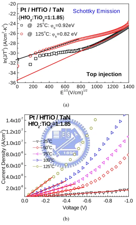
To recognize the leakage current mechanism of the HfTiO MIM capacitors, we take Schottky emission (SE) mechanism into consideration at low field. It is well known that SE mechanism, which the leakage current is electrode-limited and contributed by the carriers that overcome the barrier height between the electrode and the dielectric, has a linear ln(J/T2) - E1/2 relation as depicted by Eq. (3-2) and (3-3) [3.9, 3.10],
⎟⎟ ⎠ ⎞ ⎜ ⎜ ⎝ ⎛ − = kT T A J b /
E
ϕ
γ 12 2 * exp (3-2)⎟⎟
⎠
⎞
⎜⎜
⎝
⎛
∞ =K
e
oε
π
γ4
3 1/2 (3-3)where A* denotes the Richardson constant, k is the Boltzmann’s constant, T is the absolute temperature (K), E is the applied external electric field, e is the electron charge, εo is the permittivity in vacuum, is the high-frequency dielectric constant [3.11] (= n
∞
K
2, where n is the refractive index) and ϕ
b is corresponding to the
barrier height between metal/dielectric. Compared with the ideal Schottky barrier height (ϕ 0), the actual ϕb usually exhibits a smaller value due to image force, surface
electrode at 25 and 125oC as shown in Fig 3-9 (a) and extracted the slopes of 0.0069 and 0.0053 eV(m/V)1/2 at low field, respectively. The slopes yield the refractive index of 2.09 and 2.74 from the leakage current of 25 and 125oC, respectively. Since the refractive index of TiO2 [3.12] and HfO2 [3.13] are about 1.7-1.9 and 2.55-2.83,
respectively, the refractive index extracted at low field supports that the leakage current mechanism is probably a Schottky emission. Then we use linear extrapolation to extract the Schottky barrier height (SBH) of 0.92 and 0.82 eV at 25 and 125oC, respectively. It is well known that lower SBH at higher temperature would result in increased leakage current.
For the leakage current at very low field, the leakage current increases linearly with the increase of voltage bias as shown in Fig. 3-9 (b). It presents an Ohmic conduction mechanism, which describes the thermal excitation of trapped electrons from one trap to another at low field [3.14]. It is observed that the segment of Ohmic conduction occurred at low electric field become shorter with the temperature increasing.
Fig. 3-10 shows the Schottky emission fitting for Al/HfTiO/TaN MIM capacitors at 25 and 125oC. The linear relationship of ln(J/T2) versus E1/2 curve was obtained for Al electrode, which gives the slope of 0.00672 eV(m/V)1/2 with a refractive index of 2.18 and slope of 0.0102 eV(m/V)1/2 with a refractive index of 1.44 for 25 and 125oC, respectively. The extracted SBH for Al electrode is 0.80 eV (0.67 eV), which is slightly smaller than that of Pt electrode with 0.92 eV (0.82 eV) at 25 oC (125 oC). For Schottky barrier height, we found that the high-work-function Pt can reduce the barrier height lowering at high temperature.
is 2.5~3.9 eV, which gives the SBH between Pt/HfTiO is 1.7~3.1 eV in theory. However, the SBH of 0.92 eV at 25 oC for Pt electrode is far smaller than theoretical value and this similar result was also observed from Al case. It is suspected that little difference of SBH compared to work function difference between Pt and Al electrodes may be originated by Fermi level pinning, which describes that the work function of metals on high-κ dielectrics have been observed to differ from their values in vacuum, with the discrepancy depends on the dielectrics used [3.15-3.18]. In addition, it is suspected that the interfacial layer formed between Al electrode and HfTiO as shown in Fig. 3-2 (c) was probably another reason to modulate the SBH and enhance the overall leakage current.
To investigate the leakage current mechanism of the MIM capacitors at high electric field, the ln(J/E) versus E1/2 plots for Pt and Al electrodes are shown in Fig. 3-11 (a) and (b), respectively. The Frenkel-Poole (F-P) conduction mechanism, which is a bulk-limited current and controlled by the detrapping of the electrons from the trap centers to the conduction band of the dielectric. The F-P effect can be described asby Eq. (3-4) and (3-5) [3.7, 3.8], ⎟ ⎟ ⎠ ⎞ ⎜ ⎜ ⎝ ⎛ − = kT BE J b /
E
ϕ
γ 1 2 exp (3-4)⎟⎟
⎠
⎞
⎜⎜
⎝
⎛
∞ =K
e
ε
π
γ 0 3 1/2 (3-5)Where B is the constant and ϕb is corresponding to the trap energy level. We can
extract n values of 3.06 and 2.52 from the slopes for Pt electrode at 25 and 125oC, respectively. For Al electrode, extracted n values of 2.37 and 3.22 are obtained at 25 and
125oC, respectively. The proper n values can explain that the leakage current at high field is the F-P conduction mechanism. To extract the trapping level of HfTiO dielectric, the ln(J/E)-1/KT relationship is plotted in Fig. 3-12 (a) and (b) for Pt and Al electrodes, respectively. Trap energy for Pt and Al electrodes is 0.44 and 0.75 eV, respectively.The trap energies are less than SBH of 0.92 eV and 0.80 eV for Pt and Al cases, respectively, which supports that the conduction mechanism at high electric field were dominated by the F-P rather than SE. Apparent difference exists in the extracted trap potential height with respect to different top electrodes. This indicates that the trap at and around the interface instead of the traps at deep level in the dielectric bulk play the major role to the conduction mechanism [3.19]. It has been observed that by incorporating Al into HfO2
film, shallow trap levels will be eliminated [3.20]. In this thesis, the trapping level for Al case is deeper than that for the Pt case. It is postulated that this phenomenon may be attribute to the incorporation of Al into the HfTiO layer at the Al/HfTiO interface.
3.4 VCC Characteristics Improved by High-Work-Function Electrode
The capacitance variation with the varied bias is an important index for precision analog circuit application. The voltage dispersion of capacitance, which is also called voltage linearity, can be depicted as voltage of capacitance coefficient (VCC), which is related to the traps in bulk and interface layer [3.21]. The VCC is very important for analog or RF capacitors since high level of charge variation would result in the data loss and distortion [3.4]. Fig. 3-12 (a) shows the variation of △C(V)/C0 as a function of voltage
for Pt/[HfTiO or TiO2]/TaN capacitors. To depict the voltage nonlinearity, it has become
V V C C α β + = ∆ 2 0 (3.1) , where C0 is the capacitance at zero bias, ∆C=C(V)-C0, and α and β are quadratic and
linear coefficient of the capacitance, respectively, as determined by using a second order polynomial curve fit to measured data. The parameter of β (ppm/V), which is commonly attributed to charge repartition in the dielectrics, can be cancelled by circuit design [3.22]. It will not be studied in this thesis. Quadratic coefficient of the capacitance, α (ppm/V2
), is extracted from the C-V curve measured at 100 K to 1 MHz for a voltage range from +2
to -2 V.
From the extracted VCC-α in Fig. 3-13 (a), the mixed HfTiO dielectric not only reduces the leakage current but also improves the voltage dispersion in comparison with TiO2 dielectric. The VCC-α value can be effectively reduced from 8331 to 3730 ppm/V2
by using HfTiO dielectric to replace TiO2 dielectric. The mechanism of voltage
nonlinearity would be discussed in detail in Chapter 4.
Fig. 3-13 (b) depicts the VCC-α for Pt or Al gate at 100 KHz and 1 MHz. Using the Pt top electrode to replace Al can dramatically reduce VCC-α from 6537 to 3730 ppm/V2. It is noted that the high work function metal not only improved the leakage current but also VCC-α due to larger barrier height reducing the charges which are detraped from bulk or interfacial layer. Another possible reason for the poor VCC-α is the Al-incorporated interfacial layer as shown in Fig. 3-2 (c).
In order to understand the trap effect to VCC-α further, we try to discuss the experimental results at an elevated temperature. In Fig. 3-14 VCC characteristics of the Pt/HfTiO/TaN MIM capacitors were measured in the temperature range from 25 to 125oC at (a) 100 KHz and (b) 1 MHz. The results show that the VCC-α increases with the
temperature from 25 to 125oC. It could be expected that the higher charge trapping/detrapping rate of dielectric at high temperature would increase the number of mobile charges to affect the VCC-α.The Fig. 3-14 (c) plotted the VCC-α as a function of temperature at the frequency range from 100 KHz to 1 MHz for HfTiO MIM capacitors. The results present that the VCC-α deceases with the frequency and increases with an elevated temperature. In general, voltage and frequency dispersion are believed to be related to the existence of traps at electrode/dielectric interface. Some slow traps can not follow the measurement AC signal and thus do not contribute to the capacitance. In this case, the VCC-α is reduced.
In addition, the temperature coefficient of capacitance (TCC) is also an important parameter since ICs usually need to be operated at elevated temperature. Fig. 3-15 (a) and (b) show the TCC characteristics of the HfTiO MIM capacitors for Pt and Al top electrodes, respectively, with frequency dispersion. A small TCC value of 95 ppm/oC for the Pt-electrode sample was extracted, while large TCC value of 379 ppm/oC for the Al-electrode sample was extracted at 100 kHz. The improvement for Pt top electrode on TCC is thought to be related with charge trapping and detrapping. The Pt-electrode sample exhibits low leakage current, i.e. less charge injection. The Al-incorporated interfacial layer of the Al-electrode sample may also contribute to the poorer TCC characteristic.An increasing trend of TCC with frequency for both Pt and Al electrode is observed. At high frequency, only the fast traps can follow the AC signal for capacitance measurement. Since the trapping/detrapping time constant decreases with the increase of temperature so that more fast traps can follow the AC signal. Hence, the TCC becomes higher at higher frequency.
3.5 Effects of N
2Plasma Treatment on Dielectrics
The N2 plasma treatment was introduced to the HfTiO dielectrics to improve the
electrical properties. With optimized N2 plasma treatment condition, a power of 20 W
under substrate temperature of 300oC, the MIM capacitors exhibit lower leakage current. In Fig 3-16 (a) the improvement of almost two orders of magnitude on the leakage current at -3 V was obtained by N2 plasma treatment for 20 and 40 sec. The leakage
current is apparently improved at negative bias than at positive bias due to nitrogen incorporation into the top surface of the HfTiO dielectric. Besides, although leakage current decreases dramatically, capacitance density and VCC-α show no apparent variation as shown in Fig. 3-16 (b) and (c), respectively.
The Fig. 3-17 shows XPS depth profile for a 51 nm-thick HfTiO dielectric with and without N2 plasma treatment for (a) whole elements within sputter time from 0 to 20 min
and (b) the Ti, Hf snd N elements within sputter time from 0 to 6 min. Nitrogen accumulating at the surface of the HfTiO is found for the dielectric with N2 plasma
treatment for 40 sec. We can observe that 5% nitrogen replace oxygen and its incorporation depth is around 6 nm estimated from the sputtering rate, as shown in Fig. 3-17 (a). Umezawa et al. [3.23] suggested an atomistic model to explain the influence of oxygen vacancies (Vo) on electron leakage current. This theory demonstrated that two N atoms occupy the nearest neighbor O sites to Vo and are likely to couple with Vo. In the result, nitrogen possesses intrinsic effect to reduce leakage current by deactivating the Vo related gap states. In addition, N atoms incorporation can reduce the diffusion of Vo due to the consideration of total energy.
The reduction of the leakage current in N2 plasma treatment samples is probably
the dielectric would increase the local electric field at the electrode/dielectric interface which enhance electron transportation and therefore degrade the leakage property. The samples treated at 20 W for 20 and 40 sec perform root mean square (rms) roughness of 0.36 and 0.57 nm, respectively, while no plasma treated samples have rms roughness of about 0.66 nm as shown in Fig. 3-18. The plasma treated samples exhibit 0.21 nm difference on roughness and only less than two times leakage current difference. The roughness of the plasma non-treated sample is only 0.9 nm higher than the 40 sec plasma treated sample but the leakage current increase by two orders of magnitude. Since the leakage current variation is not proportional to the roughness variation well, another mechanism must be considered. Yong-kuk Jeong, et al. [3.24] assumed that N2 plasma
treatment can eliminate parasitic capacitors originated from defect or depletion between top electrodes and dielectrics; moreover, Nak-Jin Seong et al. [3.25] also showed that N2
plasma can reduce leakage current due to microstructure densification. This explanation is more reasonable because the leakage current mechanism is changed by the N2 plasma
0 10 20 30 40 50 60 0 20 40 60 80 100
O
Ti
Ato m ic percent (%)Etch time (sec)
Solid line (with NH3 plasma)
Open line (w/o plasma)
Ta
(a) 0.0 0.1 0.2 0.3 0.4 0.5 0.6 0.7 with NH3 plasma w/o plasma Rms (nm ) NH3 Plasma on TaN (b)Fig. 3-1 (a) Auger depth profile of HfTiO/TaN with and without NH3 plasma on the
bottom electrode of TaN and (b) surface roughness of bottom electrode of TaN with and without NH3 plasma treatment by AFM microscopy.
HfTiO
Pt
(a)
Element Weight (%) Atomic(%)
O K 4.67 34.16 Ti K 2.32 5.67 Ta L 93.01 60.16 Totals 100.00 (b) 19 nm TaN I L
18 nm HfTiO I L~1.5nm Al I L~5.4nm TaN (c)
Fig. 3-2 (a) Cross-section TEM pattern of a 19 nm-thick Pt/HfTiO/TaN MIM capacitor, which gives the high-κ value of 37 and (b) the compositions of TaTiO interfacial layer by EDX analysis. (c) Cross-section TEM pattern of a 18 nm-thick Al/HfTiO/TaN MIM capacitor giving the high-κ value of 39.
0 500 1000 1500 2000 0 30 60 90
HfTiO
O
Ti
Hf
Normalize d Yield ChannelFig. 3-3 RBS spectra of the HfTiO dielectric. The ratio of HfO2:TiO2 is equal to 1:1.85,
-2 -1 0 1 2 16 17 18 19 20
17.6 fF/
µm
2 Ca pacit ance D ensit y ( fF/ µ m 2 ) HfTiO (HfO 2:TiO2=1:1.85) TiO 2 Voltage (V)Pt / Dielectric / TaN
@ 1MHz
17.5 fF/
µm
2 (a) -3 -2 -1 0 1 2 3 10-10 10-9 10-8 10-7 10-6 10-5 10-4 10-3 10-2 10-1 100 101Pt / Dielectric / TaN
Voltage (V)Current Density (A/cm
2 ) HfTiO (HfO2:TiO2=1:1.85) TiO 2 (b)
Fig. 3-4 (a) C-V and (b) J-V characteristics of MIM capacitors using HfTiO or TiO2 as
30 40 50 60 0 100 200 300 400 (0 0 4) Anatase HfTiO @ 600oC HfTiO @ 400oC Intensity 2θ TiO2 @ 400oC
Fig. 3-5 XRD patterns of TiO2 dielectric annealed at 400oC and HfTiO dielectric
Vacuum level 2.5~ 3.9 eV[3.2] 4.1 eV Al 3.4~3.9 eV [3.3] 4.5 eV 5.6 eV TaN Pt HfTiO TaTiO
-2 -1 0 1 2 0 5 10 15 20 25 30 35 40 (HfO2 : TiO2=1:1.85)
19.5 fF/
µm
2 Cap a cit ance Den s it y ( fF/ µ m 2 ) Pt Al Voltage (V)Top metal / HfTiO / TaN
@ 1MHz
17.5 fF/
µm
2 (a) -3 -2 -1 0 1 2 3 10-9 10-8 10-7 10-6 10-5 10-4 10-3 10-2 10-1 100 101 102 Bottom injection (HfO2 : TiO2=1:1.85)Pt
Al
Voltage (V)Current Density (A/cm
2 )
Top metal / HfTiO / TaN
Top injection
(b)
Fig. 3-7 (a) C-V and (b) J-V characteristics of HfTiO MIM capacitors with Pt or Al top
![Fig. 1-2 Bandgap as the function of relative dielectric constant for various oxides [1.26]](https://thumb-ap.123doks.com/thumbv2/9libinfo/8745692.204965/29.892.157.731.164.731/fig-bandgap-function-relative-dielectric-constant-various-oxides.webp)
![Fig. 1-3 The requirement of capacitance density for RF application verse technology node in condition of the voltage linearity < 100 ppm/V 2 [1.1]](https://thumb-ap.123doks.com/thumbv2/9libinfo/8745692.204965/30.892.247.687.117.443/requirement-capacitance-density-application-technology-condition-voltage-linearity.webp)