suppressed by either decreasing the carrier density or increasing the QW length. The differential conductance at zero bias decreases with increasing temperature in accordance with a thermal-activation model up to a well-defined cut-off temperature. We demonstrate that the activation energy, cut-off temperature, and width of the ZBA are correlated, and suggest that these features are controlled by electron scattering in QWs.
DOI:10.1103/PhysRevB.81.235316 PACS number共s兲: 73.21.Hb, 73.23.Ad, 72.10.Di
I. INTRODUCTION
In a ballistic quasi-one-dimensional共1D兲 channel, the lin-ear conductance is quantized into integer multiples of Go
= 2e2/h due to the transmission of spin-degenerate 1D sub-bands within a noninteracting electron picture.1,2 Peculiar phenomena, however, such as a 0.7 anomaly and a zero-bias anomaly 共ZBA兲, referred to as the conductance peak cen-tered at zero bias in source-drain bias spectroscopy, are often observed near the first quantization plateau and have at-tracted much attention.3,4 The 0.7 anomaly which usually accompanies a conductance reduction near the first plateau, a lowered conductance at high temperatures, was mostly at-tributed to spin-related mechanisms.4–20 One-dimensional Kondo physics was proposed to describe the experimental findings, such as the scaling of conductance to a modified Kondo form and the splitting of a zero-bias conductance peak in a parallel magnetic field.4,17–20More recently, how-ever, others have claimed that 1D Kondo physics does not fully explain the intricate behaviors of the ZBA.21–23In some devices, the splitting of a zero-bias conductance peak is ab-sent in magnetic fields as high as 10 T and at G⬍0.5Go,
where the channel is fully spin-polarized.22In a few devices, splitting occurs in magnetic fields but two split peaks can resolve back into a single peak by laterally shifting the quan-tum wire 共QW兲.22,23 Additionally, zero-bias conductance peak splitting is almost linearly dependent on the split gate voltage.23 These findings indicate that ZBA cannot be ex-plained by Kondo physics. Thus, the issue is not yet com-pletely clarified and a comprehensive understanding requires further study.
A lateral shift of the QW by electrical means changes the microscopic electric field. This raises an interesting question: how and why is the ZBA influenced by the physical proper-ties of the QW, such as width, length, or carrier density? Studies of this issue may shed light on the formation of ZBA at low temperatures as well as the conductance reduction. Recently, it was reported that backscattering in QWs can be controlled by tuning a nonuniform local potential through side gates, implying that electron scattering is sensitive to the details of the potential profile.24
Here, we focus on the source-drain bias spectroscopy and temperature-dependent differential conductance at zero bias
in the range of G⬍Go. QWs of various channel lengths and
carrier densities are studied. The ZBA is suppressed by either increasing the channel length or decreasing the electron den-sity. The temperature dependence of differential conductance at zero bias follows closely the thermal-activation behavior below the cut-off temperature. In addition, we found a cor-relation between the activation temperature, cut-off tempera-ture, and ZBA width. The results indicate that the conduc-tance reductions at finite temperatures and finite biases are affected similarly by the same physics. We suggest that elec-tron scattering plays a dominant role in both ZBA and temperature-dependent conductance.
II. EXPERIMENTAL SPECIFICATIONS
The two-dimensional electron gas 共2DEG兲 that forms at the interface of a GaAs/AlxGa1−xAs heterostructure was grown using molecular beam epitaxy at the Wiezmann Insti-tute in Israel. Shubnikov-de Haas and Hall measurements were used to determine the areal electron density n. Mobility is approximately 1.7⫻106 cm2/Vs and n is 2.4 ⫻1011 cm−2corresponding to the elastic mean-free pathᐉ of ⬃14 m at low temperatures. Electron beam lithography along with thermal deposition were used to fabricate metallic gates on 共100兲 plane of the substrate. A quasi-one-dimensional quantum wire can be formed by depleting the 2DEG ⬃93 nm beneath the negatively biased split gates pair. The length of our QWs ranges from quasizero to 5 m while the nominal gap width is kept constant at⬃0.45 m. A metallic top gate 共tp兲 was fabricated on top of the split gates, isolated by a⬃100-nm-thick dielectric layer of cross-linked polymethylmethacrylate, to control the carrier concen-tration. Measurements were performed mainly in a pumped 3He cryostat and occasionally in a dilution refrigerator with base temperatures of 0.27 K and 40 mK, respectively. Dif-ferential conductance measurement was carried out using a standard four probes ac lock-in technique at 51 Hz with a small excitation voltage of 10 V.
III. RESULTS AND DISCUSSION
When a negative voltage is applied to a pair of split gates, the potential depletes the 2DEG to form a 1D channel
result-ing in a typical quantized conductance. Conductance versus split gate voltage of four samples with different QW lengths, quasizero, 0.5, 0.8, and 2 m, are plotted in Fig. 1, reveal-ing that there are conductance plateaus due to the transmis-sion of 1D subbands for QWs. The plateaus can be aligned exactly to the integer multiples of Go by subtracting the
se-ries resistance of bulk 2DEG from the data, such as in Ref. 25by Thomas et al. Here, we present the raw data since the series resistance does not affect our results. For QWs of vari-ous lengths, quantized plateaus are well developed for L ⱕ2 m, implying that the mean-free path is much longer than the channel length. For a L = 5 m QW, the quantiza-tion steps remain the same, but the quantized conductance is lower compared with the Lⱕ2 m QWs, indicating that the QW is slightly diffusive. The presented transport for QWs with lengths less than 2 m is indeed within the ballistic regime. Occasionally, charges can be trapped in samples dur-ing the cooldur-ing process and serve as extra scatterers to de-grade conductance plateaus. This would not apply, however, to our work. The systematic behaviors reported here were obtained from 13 samples through many thermal cycles. It should be noted that transport behaviors depend on the ge-ometry of the QW inside but not outside of the channel. For example, no significant difference is noted between the T-bar and straight-bar split gates. This is reasonable because the depletion regions isolate a confined QW from the 2D electron sea.
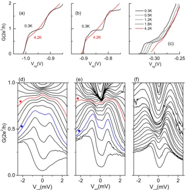
Electron transport is sensitive to carrier density, which can be effectively tuned by biasing the top gate voltage Vtpin the heterostructures, in either 1D or 2D.26Our previous work on transconductance spectroscopy, which is referred to as the half-plateau method, showed that carrier density is effec-tively changed by tuning Vtp.27In Figs.2共a兲–2共c兲, three con-ductance traces for a L = 0.5 m QW with Vtp= +0.4, −0.1, and −1.45 V at T = 0.3 K are shown as black lines. The threshold Vsgof the pinch-off voltage becomes less negative
from left to right, implying that carrier density is decreased with decreasing Vtp. Once the carrier density is substantially reduced, the quantized plateaus disappear while a qua-sishoulder appears at⬃0.5Go关Fig.2共c兲兴. Some
correspond-ing conductance traces at different temperatures are also plotted in Figs.2共a兲–2共c兲. Both Figs.2共a兲and2共b兲show that when temperature is increased from 0.3 to 4.2 K conductance decreases in the vicinity of the first plateau. A quasishoulder
forms near 0.7Go while the plateaus are washed out. The
phenomenon is a typical feature of the 0.7 anomaly.4For the same QW with more negative Vtpin Fig.2共c兲, conductance traces at different temperatures remain almost the same. No-tice that the curves of higher temperatures are horizontally shifted for clarity in Fig. 2共c兲. As expected, conductance is not sensitive to temperature in the sample with low carrier density while a clear temperatuinduced conductance re-duction around 0.7Gooccurs in the sample with high carrier
density.25
We investigated the source-drain bias spectroscopy by sweeping a dc source-drain voltage Vsd across a confined
QW and measuring the differential conductance G = dI/dVsd.
Figures2共d兲–2共f兲show the spectroscopies G共Vsd兲 against Vsg
of this sample for the three identical top gate voltages at T = 0.3 K. For Vtp= +0.4 V in Fig. 2共d兲, the differential con-ductance exhibits clearly a series of single peak centered at
Vsd= 0 for G⬍Go referring to as ZBA, e.g., the star-labeled
and the neighboring curves. The feature is novel and distin-guishable from the bell-shaped structure of the nonlinear conductance of the transmission of the subbands.28Based on the source-drain bias spectroscopies of numerous samples at a series of Vtp, ZBA becomes weaker with decreasing carrier density. Specifically, the ZBA at Vtp= −0.1 V 关Fig. 2共e兲兴 is narrower than at Vtp= +0.4 V关Fig.2共d兲兴, and disappears
en-FIG. 1. G共Vsg兲 and micrographs of QWs of various lengths: 共a兲
quasizero,共b兲 0.5 m, 共c兲 0.8 m, and 共d兲 2 m. The scale bars 共white bars in the insets兲 indicate a length of 0.5 m. The top gate is grounded for all four data sets.
FIG. 2. 共Color online兲 关共a兲–共c兲兴 Zero-bias differential conduc-tance versus split gate voltage of a L = 0.5 m QW for Vtp=共a兲 + 0.4 V,共b兲 −0.1 V, and 共c兲 −1.45 V, respectively, at various tem-peratures. 关共d兲–共f兲兴 Source-drain bias spectroscopies of the same sample at the same top gate voltages at 0.3 K.共d兲 Vtp= +0.4 V. Vsg
is from −938 to −1002 mV in 4 mV steps. Star- 共red兲 and dot-共blue兲 labeled traces indicate Vsg= −970 and −986 mV,
respec-tively. 共e兲 Vtp= −0.1 V. Vsg is from −819 to −900 mV in 3 mV
steps. Star- 共red兲 and dot- 共blue兲 labeled traces indicate Vsg= −873 mV and −891 mV, respectively. 共f兲 Vtp= −1.45 V. Vsg is
tirely at Vtp= −1.45 V关Fig.2共f兲兴. We characterize the width of a ZBA by⌬VsdZBA, the source-drain voltage difference
be-tween the “peak” and the “bottom” of the ZBA. From the star-labeled curve to the dot-labeled curve in Fig. 2共d兲, ⌬VsdZBA decreases from⬃750 to ⬃280 V with decreasing Vsg. Beyond the dot-labeled curve, the ZBA is absent for Vsg⬍−986 mV. Similar trend holds in Fig.2共e兲. The width
drops from⬃250 V共the star-labeled curve兲 to ⬃160 V 共the dot-labeled curve兲 and the ZBA disappears for Vsg⬍
−891 mV. As to the sample with the lowest carrier density in Fig.2共f兲, no ZBA is present for all split gate voltages. The observations evidence that ZBA is suppressed by decreasing the carrier density.
A robust 0.7 anomaly along with the absence of ZBA in ultralow-disordered QWs was reported by Reilly et al.12 They suggested that carrier-density-induced enhancement in spin-splitting results in a spin gap.12 Our observation of the systematic evolution of ZBA with respect to carrier density inspires an alternative thought. From electron-electron inter-action 共EEI兲 perspective, a system of lower carrier density has, in general, stronger EEI. It was well established that EEI contributes a Coulomb anomaly in the density of states which brings about a tunneling conductance gap at T = 0 and a negative tunneling conductance cusp at finite temperatures.29,30This could suppress the ZBA in a low car-rier density QW. One would expect that the ZBA depends on QW geometry which affects EEI. To investigate the influence of QW length on the effect, we systematically studied the source-drain bias spectroscopies of QWs with quasizero ⱕLⱕ5 m.
The results presented in Fig.2imply that there will be a weak but nonzero ZBA for a L = 0.5 m QW at Vtp= 0 V. Here, we present G共Vsd兲 against Vsgfor other four samples
with L = quasizero, 0.25, 0.8, and 2 m, at Vtp= 0 and T = 0.3 K in Fig. 3. The L = quasizero QW has a very strong ZBA. In Fig. 3共a兲, ⌬Vsd
ZBA
decreases from ⬃1.2 mV 共the star-labeled curve兲 to ⬃290 V共the dot-labeled curve兲 with decreasing Vsg. The L = 0.25 m QW has a slightly weaker
ference in ZBA among our QWs in the range of 0.2– 0.5 m. By also including the data for the quasizero and longer QWs, however, we provide a full picture of the evolution of ZBA with respect to QW length. The L ⱕ2 m QWs are at least a few times shorter than the mean-free path and hence, the diffusive scattering is negligible. In all of these samples, the differential conductance traces at zero-bias demonstrated many clear quantized conductance plateaus. There is neither superimposed resonance peak nor distorted plateau in G共Vsg兲. This feature is robust to thermal
cycling, indicating that the ballistic transport is not affected. It has been suggested that spin polarization can be enhanced in long QWs to split the ZBA.8,11 In our long QWs, we did not observe any splitting of the zero-bias conductance peak. We suggest that the increase in QW length allows for addi-tional scattering of conducting electrons, which results in enhanced EEI and correspondingly, a diminished ZBA. For the L = 5 m QW, the lowered quantized conductance could be attributed to diffusive scattering. As the conductance quantization is sustained, however, the transport is mostly ballistic. In this case, we believe that the increased channel length still plays a dominant role in suppressing ZBA.
One more interesting phenomenon is that ZBA seems to be accompanied by a temperatuinduced conductance re-duction for G⬍Go. Figure2shows the representing behavior
for all other samples in the study of carrier density effect. Here, we determine if there is a correlation between the ZBA and the temperature-induced conductance reduction. We plot three G共T兲 traces of a L=quasizero QW in the inset of Fig. 4共a兲to show the typical temperature-dependent conductance behavior. The zero-bias differential conductance decreases with increasing temperature. Although temperature depen-dence of the 0.7 anomaly has been intensively studied for quite some time, the results vary widely.4,21,22,32,33 Among them two types were mostly proposed, Kondo-type,4and ac-tivated temperature-dependent behaviors.21,22,32,33Numerical fittings using both Kondo-type4and thermal-activation mod-els to the data are shown as dashed and solid lines in the inset of Fig. 4共a兲, respectively.34 Both models seem to de-scribe experimental results well at low temperatures. The applicable temperature range, however, is wider and the fit-ting parameters obtained from the fit exhibit a systematic variation in the activation model. Hence, we adopted the activation model to analyze the data.
The temperature-dependent conductance based on the thermal-activation model is expressed as G共T兲=G共0兲
共1−Ce−Ta/T兲 where G共0兲 is the measured conductance at the base temperature. Ta and C are the fitting parameters.32
Re-arranging the equation, fadefined as
1
C关1− G共T兲
G共0兲兴 equals e
−Ta/T. Semilogarithmic plots of fa versus Ta/T for a L=quasizero FIG. 3. 共Color online兲 Source-drain bias spectroscopies of QWs
of several lengths at 0.3 K for Vtp= 0.共a兲 L=quasizero. From top to
bottom, Vsg decreases from −1450 to −1558 mV in 4 mV steps. Star- and dot-labeled traces indicate Vsg= −1498 共red兲 and
−1526 mV共blue兲, respectively. 共b兲 L=0.25 m. Vsgis from −914 to −1002 mV in 4 mV steps.共c兲 L=0.8 m. Vsgis from −570 to
−612 mV in 2 mV steps. 共d兲 L=2 m. Vsg is from −810 to −858 mV in 2 mV steps.
QW against a series of Vsgat Vtp= 0 are presented in Fig.4共a兲 to confirm the typical thermal-activation behavior. After scal-ing T by Tain this semilogarithmic Arrhenius plot, all traces
generally collapse onto a universal curve following a linear relation down to ⬃0.2Ta共Ta/T⬃5兲. The dashed line is the
least-square-root linear fit. Thermal-activation behavior is valid up to a “cut-off” temperature, Tc. In Fig.4共a兲, traces of fashow a downward trend deviating from the linear fit at low
values of Ta/T. Tc was determined by finding the
tempera-ture at which the data begins to deviate from the fit. As an example, Tcfor three Vsgis labeled in the inset of Fig.4共a兲.
The evolution of Tc with respect to either Vsg or G共0兲 is
obtained for G⬍Go. As G共0兲 decreases, Tcdecreases and so
does Ta. Taincreases with increasing Vsgfrom sub-Kelvin for G共0兲⬃0.5Go, to a few Kelvin in the vicinity of the first
plateau. The activation temperature, as a function of Vsgfor
three samples, is shown in Figs. 4共b兲–4共d兲. Other samples, except those with either low carrier density or long channel length, exhibit similar behavior with an exponential depen-dence of the activation energy on split gate voltage, which is consistent with previous experimental findings by other groups.21,22 Bruus et al.33 proposed that the observed acti-vated behavior in G is related to the thermal depopulation of a subband with a gate-voltage-dependent subband edge. The power-law relation between the activation energy and split gate voltage was experimentally obtained by Bruus et al.32,33 It is quite interesting that there is not only a correlation between Taand Tc, but also a close relation between Taor Tc
and the ZBA width for Gⱗ0.9Go. The relations can be
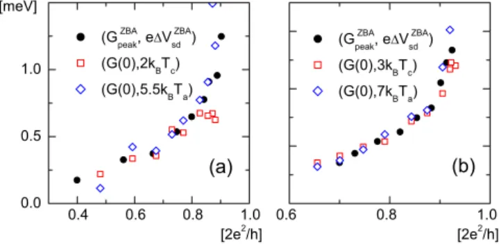
clearly demonstrated by scaling关G共0兲, Tc兴, 关G共0兲, Ta兴
ex-tracted from the temperature-dependent conductance, and 共Gpeak
ZBA,⌬V
sd
ZBA兲 extracted from the source-drain bias spectros-copy on the same plot as shown in Figs. 5共a兲 and5共b兲 for
two L = quasizero QWs. Gpeak
ZBA
is the conductance at the ZBA peak at the base temperature. In Fig. 5共a兲, three traces of 关G共0兲, 2kBTc兴, 关G共0兲, 5.5kBTa兴, and 共Gpeak
ZBA, e⌬V
sd
ZBA兲 col-lapse onto one curve for one sample. Likewise in Fig. 5共b兲, three traces of 关G共0兲, 3kBTc兴, 关G共0兲, 7kBTa兴, and 共GpeakZBA, e⌬VsdZBA兲 collapse also onto one curve for the other sample.
Although the factors are slightly different, the scenario is robust. Three characteristic quantities, Tc, Ta, and ⌬VsdZBA,
decrease monotonically with decreasing zero-bias differential conductance.
While the 0.7 anomaly manifests at high temperatures, it is also observable at finite source-drain biases at low tem-peratures, seen as bunches of curves, e.g., for 兩Vsd兩
ⲏ0.6 mV in Figs.3共a兲and3共b兲. For a specific Vsg,
increas-ing 兩Vsd兩 from zero-bias reduces the conductance while the
relation of G versus Vsd forms the ZBA. The fact that the
three traces obtained from two different measurements match suggests that the temperature- and bias-induced conductance reductions are strongly correlated.
Theoretical works suggested that conductance decreases with increasing energy scale共either bias voltage or tempera-ture兲 under the consideration of backscattering.35,36 Increas-ing either the bias or temperature enlarges the momentum space of integration and henceforth increases backscattered current or resistance. Calculations showed that multiple-electron backscattering becomes frequent as the source-drain bias increases, leading to a reduced conductance, manifesting as ZBA, whereas enhanced EEI prompts strong multiple-electron scattering to weaken the ZBA.35,37 On the other hand, several groups have suggested that electron-electron scattering brings about a reduced conductance at elevated temperatures.16,35,37–40The temperature-induced conductance correction was suggested to follow an activation law.38 Thermal-activated dependence of conductance can also be predicted by taking the backscattering of electrons mediated by acoustic phonons into account.36 The same mechanism can describe the negative correction to conductance by the finite source-drain bias in ZBA as well. The theoretical pro-posals provide a picture that electron backscattering results in ZBA and temperature-dependent conductance, which may explain our results.
Comparing the spectroscopies reported in Refs.4,22,23, 32, and 41, the shape, amplitude, and width of the ZBA
FIG. 4.共Color online兲 共a兲 Semilogarithmic plot of favs Ta/T for
a L = quasizero QW against a series of Vsgat Vtp= 0.共see text兲 The dashed line is the least-square-root linear fit. Inset: three typical traces of measured G共T兲, along with the simulated curves of the activation model共solid lines兲 and Kondo-type model 共dashed lines兲 共Ref. 34兲. The cut-off temperature at which G共T兲 deviates from activation behavior is located and indexed as Tci for a split gate voltage Vsgi .关共b兲–共d兲兴 Activation temperature vs split gate voltage at
Vtp= 0 for 共b兲 and 共c兲 two L=quasizero QWs and 共d兲 a L
= 0.5 m QW. Lines were fitted using the linear least-square-root regression method.
FIG. 5. 共Color online兲 共GZBApeak, e⌬VsdZBA兲, 关G共0兲, scaled Tc兴, and
We provide evidence that ZBA depends systematically on physical properties of QWs. The amplitude and width of the ZBA decrease with either decreasing carrier density or in-creasing channel length, wherein the scattering rate of elec-trons is expected to increase. The ZBA is totally suppressed by strong scattering, in a either very low carrier density or long QW. The activation model is preferable for describing
ACKNOWLEDGMENTS
We have benefited from discussions with C. S. Chu, J. H. Hsiao, P. J. Lin, and L. Y. Wang. We thank J. M. Valles, Jr. for a critical reading of the manuscript. This work was sup-ported by NSC grant in Taiwan under Project No. NSC96-2112-M-009-030-MY3 and MOE ATU program.
1D. A. Wharam, T. J. Thornton, R. Newbury, M. Pepper, H.
Ahmed, J. E. F. Frost, D. G. Hasko, D. C. Peacock, D. A. Ritchie, and G. A. C. Jones,J. Phys. C 21, L209共1988兲.
2B. J. van Wees, H. van Houten, C. W. J. Beenakker, J. G.
Will-iamson, L. P. Kouwenhoven, D. van der Marel, and C. T. Foxon, Phys. Rev. Lett. 60, 848共1988兲.
3K. J. Thomas, J. T. Nicholls, M. Y. Simmons, M. Pepper, D. R.
Mace, and D. A. Ritchie,Phys. Rev. Lett. 77, 135共1996兲.
4S. M. Cronenwett, H. J. Lynch, D. Goldhaber-Gordon, L. P.
Kou-wenhoven, C. M. Marcus, K. Hirose, N. S. Wingreen, and V. Umansky,Phys. Rev. Lett. 88, 226805共2002兲.
5R. Akis and D. K. Ferry,J. Phys.: Condens. Matter 20, 164201
共2008兲.
6A. A. Starikov, I. I. Yakimenko, and K. F. Berggren,Phys. Rev.
B 67, 235319共2003兲.
7K. F. Berggren and I. I. Yakimenko,Phys. Rev. B 66, 085323
共2002兲.
8P. Jaksch, I. Yakimenko, and K. F. Berggren,Phys. Rev. B 74,
235320共2006兲.
9A. Lassl, P. Schlagheck, and K. Richter, Phys. Rev. B 75,
045346共2007兲.
10P. Havu, M. J. Puska, R. M. Nieminen, and V. Havu,Phys. Rev.
B 70, 233308共2004兲.
11D. J. Reilly, G. R. Facer, A. S. Dzurak, B. E. Kane, P. J. Stiles,
R. G. Clark, A. R. Hamilton, J. L. O’Brien, N. E. Lumpkin, L. N. Pfeiffer, and K. W. West, Phys. Rev. B 63, 121311共R兲 共2001兲.
12D. J. Reilly, T. M. Buehler, J. L. O’Brien, A. R. Hamilton, A. S.
Dzurak, R. G. Clark, B. E. Kane, L. N. Pfeiffer, and K. W. West, Phys. Rev. Lett. 89, 246801共2002兲.
13D. J. Reilly,Phys. Rev. B 72, 033309共2005兲. 14Y. Tokura and A. Khaetskii,Physica E 12, 711共2002兲. 15K. A. Matveev,Phys. Rev. B 70, 245319共2004兲. 16K. A. Matveev,Phys. Rev. Lett. 92, 106801共2004兲.
17Y. Meir, K. Hirose, and N. S. Wingreen, Phys. Rev. Lett. 89,
196802共2002兲.
18K. Hirose, Y. Meir, and N. S. Wingreen, Phys. Rev. Lett. 90,
026804共2003兲.
19T. Rejec and Y. Meir,Nature共London兲 442, 900 共2006兲. 20J. H. Hsiao, K. M. Liu, S. Y. Hsu, and T. M. Hong,Phys. Rev. B
79, 033304共2009兲.
21F. Sfigakis, C. J. B. Ford, M. Pepper, M. Kataoka, D. A. Ritchie,
and M. Y. Simmons,Phys. Rev. Lett. 100, 026807共2008兲.
22T. M. Chen, A. C. Graham, M. Pepper, I. Farrer, and D. A.
Ritchie,Phys. Rev. B 79, 153303共2009兲.
23S. Sarkozy, F. Sfigakis, K. Das Gupta, I. Farrer, D. A. Ritchie, G.
A. C. Jones, and M. Pepper, Phys. Rev. B 79, 161307共R兲 共2009兲.
24D. Hartmann, L. Worschech, and A. Forchel,Phys. Rev. B 78,
113306共2008兲.
25K. J. Thomas, J. T. Nicholls, M. Pepper, W. R. Tribe, M. Y.
Simmons, and D. A. Ritchie,Phys. Rev. B 61, R13365共2000兲.
26B. E. Kane, G. R. Facer, A. S. Dzurak, N. E. Lumpkin, R. G.
Clark, L. N. Pfeiffer, and K. W. West, Appl. Phys. Lett. 72, 3506共1998兲.
27K. M. Liu, H. I. Lin, V. Umansky, and S. Y. Hsu,Physica E 42,
1122共2010兲.
28L. Martin-Moreno, J. T. Nicholls, N. K. Patel, and M. Pepper,J.
Phys.: Condens. Matter 4, 1323共1992兲.
29B. L. Altshuler and A. G. Aronov, Sov. Phys. JETP 48, 812
共1979兲.
30T. Morimoto, M. Henmi, R. Naito, K. Tsubaki, N. Aoki, J. P.
Bird, and Y. Ochiai,Phys. Rev. Lett. 97, 096801共2006兲.
31E. J. Koop, A. I. Lerescu, J. Liu, B. J. van Wees, D. Reuter, A.
D. Wieck, and C. H. van der Wal,J. Supercond. Nov. Magn. 20, 433共2007兲.
32A. Kristensen, H. Bruus, A. E. Hansen, J. B. Jensen, P. E.
Lin-delof, C. J. Marckmann, J. Nygård, C. B. Sørensen, F. Beuscher, A. Forchel, and M. Michel,Phys. Rev. B 62, 10950共2000兲.
33H. Bruus, V. Cheianov, and K. Flensberg, Physica E 10, 97
共2001兲.
34The Kondo-type model for a quantum wire: G KL共T兲
= G共0兲关1/兵2关1+共21/s− 1兲共T/TKL兲2兴−s其+1/2兴, where s=0.22.
Al-though numerical fit using this model can describe part of data, there is no systematic relation between the fitting parameter TKL
and split gate voltage.
35A. M. Lunde, A. De Martino, A. Schulz, R. Egger, and K.
Flens-berg,New J. Phys. 11, 023031共2009兲.
36G. Seelig and K. A. Matveev, Phys. Rev. Lett. 90, 176804
共2003兲.
37D. Meidan and Y. Oreg,Phys. Rev. B 72, 121312共R兲 共2005兲. 38A. M. Lunde, K. Flensberg, and L. I. Glazman,Phys. Rev. B 75,
245418共2007兲.
39D. Schmeltzer, A. Saxena, A. R. Bishop, and D. L. Smith,Phys.
Rev. B 71, 045429共2005兲.
40J. Rech and K. A. Matveev, Phys. Rev. Lett. 100, 066407
共2008兲.
41J. C. Chen, Y. Lin, K. T. Lin, T. Ueda, and S. Komiyama,Appl.
![TraditionalMLCalgorithmsmainlytacklethebatchMLCproblem,wheretheinputdataarepresentedinabatch[24,28].Nevertheless,inmanyMLCapplicationssuchase-mailcategorization[22],multi-labelexamplesarriveasastream.Onlineanalysisistherefore dimensionreducermotivatedbyma](data:image/gif;base64,R0lGODlhAQABAIAAAP///wAAACH5BAEAAAAALAAAAAABAAEAAAICRAEAOw==)