Fast Transistor Threshold Voltage Measurement
Method for High-Speed, High-Accuracy
Advanced Process Characterization
Tseng-Chin Luo, Mango C.-T. Chao, Huan-Chi Tseng, Masaharu Goto, Philip A. Fisher, Yuan-Yao Chang,
Chi-Min Chang, Takayuki Takao, Katsuhito Iwasaki, and Cheng Mao Lee
Abstract— As process technologies continually advance, process variation has greatly increased and has gradually become one of the most critical factors for IC manufacturing. Further-more, these increasingly complex processes continue to make greater use of stressors for mobility enhancement, thus requiring large volumes of data for extensive characterization of layout-dependent effects (LDE) for validation of both SPICE models and design for manufacturing. Transistor threshold voltage (Vt)
is a commonly used parameter both for characterization during process development and for monitoring of volume manufac-turing. To adequately quantify local process variation or LDE, Vt must be measured for a sufficiently large number of
device-under-tests (DUTs) to obtain a statistically representative sample population. The number of Vt measurements required to obtain
such a statistically significant result, however, requires extremely long testing time, especially for array-based test structure designs including thousands of DUTs. In this paper, we present a very fast threshold voltage measurement methodology using an operational amplifier-based source-measure unit test configuration, which greatly improves testing efficiency and accuracy, and is not sensitive to process variation. The proposed test methodology can improve Vt testing time by a factor of 5–10 relative to the
commonly used binary-search algorithm, and by a factor of ∼2 relative to an optimized interpolation algorithm, and achieves better accuracy (standard deviation of Vt = 0.15 mV, versus
typical accuracy of∼ 0.5 mV for the two algorithms mentioned). Furthermore, the layout and configuration of conventional test structures need not be modified to adapt the proposed method-ology. The measured results from the most advanced process technology nodes demonstrate the testing efficiency and accuracy of the proposed test structure in characterizing the large number of DUTs required for quantifying process variation or LDEs.
Index Terms— Design for manufacturing (DFM), Threshold voltage, Variation,
Manuscript received May 6, 2012; revised September 29, 2012 and February 19, 2013; accepted May 9, 2013. Date of publication July 9, 2013; date of current version April 22, 2014.
T.-C. Luo is with Taiwan Semiconductor Manufacturing Corporation, Hsinchu 30077, Taiwan, and also with the Department of Electronics Engi-neering and Institute of Electronics, National Chiao Tung University, Hsinchu 300, Taiwan (e-mail: tclo@tsmc.com).
M. C.-T. Chao is with the Department of Electronics Engineering and Institute of Electronics, National Chiao Tung University, Hsinchu 300, Taiwan (e-mail: mango@faculty.nctu.edu.tw).
H.-C. Tseng, P. A. Fisher, Y.-Y. Chang, and C.-M. Chang are with Taiwan Semiconductor Manufacturing Corporation, Hsinchu 30077, Taiwan (e-mail: hctseng@tsmc.com; philip_a_fisher@yahoo.com; yychangn@tsmc.com; cmchangu@tsmc.com).
M. Goto, T. Takao, K. Iwasaki, and C. M. Lee are with Agilent Technologies, Tokyo 192-8510, Japan (e-mail: masaharu_goto@ agilent.com; takayuki_takao@agilent.com; tatsuhito_iwasaki@agilent.com; chiso_lee@agilent.com).
Color versions of one or more of the figures in this paper are available online at http://ieeexplore.ieee.org.
Digital Object Identifier 10.1109/TVLSI.2013.2265299
I. INTRODUCTION
A
S THE feature size of devices scales down, the device variability imposed by each process step does not scale accordingly. Therefore, the process variation of advanced process technology nodes greatly increases and becomes a critical factor in both IC design and manufacturing [1]. To design and manufacture in the presence of process varia-tion, many research efforts have been focused on the areas of measurement, analysis, and modeling of variation during the past decade [2]–[9], [12]. Furthermore, modeling and design for manufacturing (DFM) of increasingly complex process technologies incorporating process features such as stressed contact etch-stop layers, SiGe source/drain [9], stress memorization technique [11], and so forth requires a much larger range of test structures and larger data volume to accurately characterize the layout-dependent effects (LDE) resulting from these process features. The need to accurately characterize both process variation and increasing complex LDE has dramatically increased the number of testing required during all stages of process development and manufacturing, which in turn demands the development of more efficient test structures and methods that can provide this data without increasing test time to unfeasible levels. During conventional device characterization for the study of LDE and process variation, a conventional test structure, i.e., a process control monitor (PCM) testline, is placed in a wafer’s scribe line. The PCM testline has device-under-tests (DUTs) and I/O pads aligned along a straight line and uses four I/O pads to measure each DUT. Thus, both the height of a PCM testline and the required spacing in a scribe line are lim-ited [19]. Only a relatively limlim-ited number of DUTs can be placed in such a testline configuration because of the limited number of I/O pads. To effectively use limited scribe-line space to place and individually measure a sufficiently large number of DUTs to address the characterization needs of DFM, LDE, and process variation, several array-based test structures are proposed to share I/O pads among DUTs and hence reduce the number of I/O pads required between the DUTs [13], [15], [16].Transistor threshold voltage (Vt) is a commonly used parameter to quantify transistor performance both during process development and volume manufacturing [20]. There are several different definitions of the threshold voltage of a metal oxide semiconductor field-effect transistor (MOSFET)
1063-8210 © 2013 IEEE. Personal use is permitted, but republication/redistribution requires IEEE permission. See http://www.ieee.org/publications_standards/publications/rights/index.html for more information.
ingful results, and the Vt measurements represent the most time-consuming portion of the characterization of these DUTs.
Operational amplifier (op-amp or OP)-based methods were proposed to simplify and accelerate Vt measurement [21]. Recently, the research of [23] has also proposed similar methods, employing an on-chip op-amp design combined with an addressable FET array. Such op-amp schemes enable rapid characterization of Vt distributions with large numbers of data samples. There are, however, several major challenges in on-chip OP-based amplifier design for Vt measurement. First, the
Vt measured by OP-based test structures may be impacted by body effect because of nonzero source voltage, e.g., as would occur in the circuit of [23]. Second, variation of on-chip load resistance (Rload) can result in an inaccurate Vt measurement. This latter issue will become much more severe in modern advanced process technology nodes because of the scaling of feature size without corresponding scaling of variability. Finally, schemes using on-chip OP-based structures are limited by the op-amp accuracy and gain. In 0.35-µm technology, an OP gain of 100 dB is easily achieved using folded cascode design. The gain, however, decreases significantly in advanced technologies because of small transistor output resistance and reduction in headroom. In such advanced technologies, the design of op-amps with gain as high as 100 dB requires additional circuitry. Therefore, the layout area devoted to the op-amp significantly increases, which might prevent the design of practical testlines that can be placed within the wafer scribe line. Furthermore, device mismatch is very poor in the early stages of process development. Therefore, there may be substantial errors in the Vt measured by on-chip OP-based test structures during the early stages of process development.
In this paper, we propose a design and methodology for
Vt measurement using high gain and high accuracy op-amp-based Source-Measure Units(SMUs) directly connected to the DUT. The OP-based SMUs are implemented using discrete ICs which are well calibrated by the tester supplier, and thus are not sensitive to process variation. The experimental results that we present, based on advanced process technolo-gies, demonstrate that the proposed design reduced Vt testing time by a factor of 5–10 relative to the conventional binary search Vt measurement algorithm, while simultaneously deliv-ering improved accuracy, with a Vt standard deviation below 0.15 mV. Moreover, combined with array-based test structure, the test time can be further improved due to time overhead saving from the connect, disconnect operation between SMUs and testlines I/O pads and prober index time, which is prober chuck moving time from one testline to another.
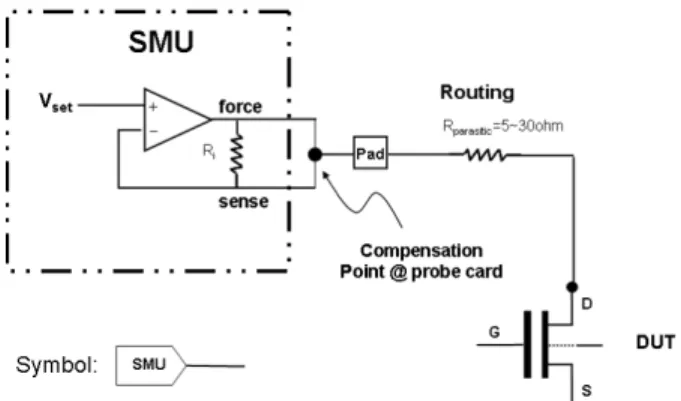
Fig. 1. Voltage compensation mechanism used in a conventional PCM testline. Hereafter, each SMU will be denoted by the symbol indicated in the lower left of the figure.
Another valuable example for the use of array-based test structures to characterize the statistical variation of a large number of transistors was contained in the research of [17], wherein a combination of an array of individually addressable identical devices was combined with an innovative comparator-based measurement scheme was used to extract the difference in the Vt of each device in the array compared with a reference transistor, and thus to determine the statistical distribution of Vt throughout the entire array. This technique was quite effective for quantifying the statistical distribution of Vt for a particular device layout, but because the quan-tity directly measured was the difference between the Vt of the addressed DUT and a reference transistor, the structure was limited to characterization of the statistical variation of multiple transistors with the same geometry and layout of the reference device. In contrast, the test structure we present can directly measure the dc transistor characteristics of each addressed device in the array, and thus does not require a reference device, and can accommodate multiple device geometries within the same array. The direct measurement of each addressed device without use of a reference also avoids measurement errors induced by deviations in the peripheral circuitry such as source follower mismatch. Finally, although the research of [17] constitutes a quite ingenious method of measuring the statistical variation of Vt, its principle focus was on Vt measurement, whereas the method we propose here-in can be readily extended to other standard transistor parametrics (e.g., Idsat, Ioff, etc.,) because the key measurement
infrastruc-ture is off chip.
II. BACKGROUND
A. Measuring Constant Current Vt Using a Binary Search
Algorithm
In a traditional parametric tester Vt measurement, the SMUs are configured as voltage sources, which can be modeled as unity-gain buffers as shown in Fig. 1 [19]. Vt can be defined as the gate-to-source potential required to drive the threshold drain-to-source current, Ids(Vt) = (I0, n)∗Weff/Leff for n-FET, and Ids(Vt) = (I0, p)∗Weff/Leff for p-FET, where I0, n and I0, p are parameters of a given process technology for n-FET and p-FET, respectively. In this paper, we use I0 = 20 nA/µm for both N and pMOS. Before beginning the binary
Fig. 2. SMU connection and bias condition for Vt measurement using a
binary search approach for n-FET.
search for Vt measurement, the following parameters of the binary search must be specified: 1) gate voltages Vgstart and Vgstop, which specify the range of gate voltages to be searched and 2) a convergence criteria for matching the target current. In the first iteration, SMU2 forces the search voltage value,
Vforce= (Vgstart+Vgstop)/2, to the gate node of the DUT while
SMU1 measures the drain current (Ids) and compares it with
the target value. If the matching criteria(Ids− Itarget)/Itarget< matching tolerance, is met, Vt is assigned to Vforce. If it is,
however, larger than the matching criteria, another iteration must be performed. Before proceeding to the next iteration,
Vforce must be modified. If Ids> Itargetthen SMU2 forces the
search voltage value Vforce = (Vgstart+ Vforce)/2. In contract,
if Ids < Itarget then SMU2 forces the search voltage value Vforce= (Vforce+ Vgstop)/2.
In subsequent iterations, the SMU2 applies gate voltage val-ues above and below Vt, which become increasingly close to
Vt with successive iterations until the current measured by the sense unit matches the target value within the specified criteria. Fig. 3 lists the pseudo-code implementation of a binary search algorithm for finding the gate voltage resulting in a specified drain current. The accuracy of the result obtained by this algo-rithm strongly depends on the convergence condition and the maximum number of iterations, which thus presents a trade-off between testing time and accuracy. Fig. 4 schematically shows the iteration of forcing voltage and measuring current for Vt measurement using the binary search algorithm.
Therefore, the binary search algorithm for Vt measure-ment typically requires much longer testing time than the measurement of other device parametrics such as Ion, Ioff,
and subthreshold swing. For the measurement of a number of DUTs large enough to obtain a statistically significant quantification of process variation, or to perform adequate characterization for LDE modelling or DFM verification, the
Fig. 3. Pseudocode of binary search Vtmeasurement.
Fig. 4. Example of iterating Vgto obtain drain current matching target within
specified criteria.
test time correspondingly increases and may limit the number of DUTs that can be measured, thus also limiting the accuracy of the characterization.
B. Improving Constant Current Vt Testing Time Using an
Interpolation Methodology
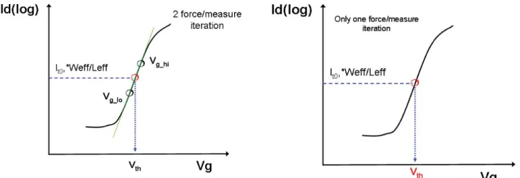
One approach to reduce the number of SMU force-measure iterations below the number required by the binary search algorithm is to apply an interpolation algorithm. The number of force-measure iterations can be reduced from six to nine iterations for the binary search algorithm to three iterations for the interpolation algorithm. The interpolation method is performed by setting the two initially defined gate voltages, Vg_hi and Vg_lo, to corresponding drain current values very close to the target current (e.g., I 0, n∗Weff/Leff for n-FET). To minimize the interpolation error, one gate voltage is set to
Fig. 5. Setting the initial gate voltage values to interpolate to the gate voltage corresponding to the target drain current. Log scale is used only for ease of visualization. In practice, linear scale is used for Vt interpolation.
Fig. 6. Double-hump transistor I –V curve resulting from use of STI. (a) Cross-section of a transistor perpendicular to the channel length, including both the region where the gate lies over the active area (AA), i.e. the Main Device, and the two Corner Devices where the gate lies over the transition region between active area and STI. (b) Individual I –V characteristics of the main and corner devices. (c) I –V characteristic of the entire transistor including both main and corner devices. The two local maxima of Id, i.e. the “double hump” characteristic potentially results in very different values of Vt by the binary search and interpolation techniques.
drive a drain current slightly higher than the target current, and the other gate voltage drives a drain current slightly lower than the target, as shown in Fig 5. The Vt value can be simply obtained by interpolation because of the linear I –V characteristics in the subthreshold region. This interpolation methodology is easily applied to measure the variation of DUTs with identical or nearly identical dimensions because the same initial voltage settings and current criterion can be used for all DUTs. However, for the characterization of many DUTs with different transistor dimensions, e.g., for DFM, SPICE modeling or other process characterization, it may be difficult to define initial gate voltages appropriate to all DUTs. Moreover, in the case of a MOSFET fabricated using shallow-trench-isolation (STI), the gate region runs flat across the isolation. Therefore, the portion of the gate over the field region creates a two-dimensional fringing field on the corner and sidewall region as shown in Fig. 6(a), which effectively creates a corner parasitic MOSFET in parallel with the main DUT. The parasitic device turns on at a gate voltage lower than that of the main DUT channel, resulting in a hump in the
Id–Vgcurve as shown in Fig. 6(b) [22]. As shown in Fig. 6(c), a MOSFET with such a hump in its Id–Vg characteristic exhibits a significant difference between the values of Vt obtained by interpolation and binary search methodologies, respectively. Therefore, this interpolation technique cannot be applied to devices exhibiting nonlinear I –V characteristics in the subthreshold region, such as those with parasitic corner
Fig. 7. Only a single force-measure iteration is required by the OP-based
Vt measurement technique.
Fig. 8. Circuit schematics for OP-based Vt measurement, where the DUT
is (a) n-FET and (b) p-FET.
devices resulting from STI. As STI is a common feature of almost all modern CMOS technologies, this severely limits the utility of the interpolation technique.
C. Fast Vt Measurement Using an On-Chip Op-Amp-Based
Test Structure
Although the number of force-measure iterations can be reduced from∼9 for binary search to two for the interpolation algorithm as described above, the Vt value obtained by the interpolation algorithm is less accurate than that obtained by binary search. The number of force-measure iterations for constant current Vt measurement can actually be fur-ther reduced to only a single iteration, while maintaining higher measurement accuracy, by adopting op-amp-based test structures using an on-chip op-amp. This technique for Vt measurement using only one force-measure iteration is shown in Fig. 7. Fig. 8 shows the circuit schematics for the op-amp-based test structure for Vt measurement. In Fig. 8(a), Vset, Vss, Vb, and Vd are input terminals and Vg is the op-amp output, which is connected to both the DUT gate and a digital voltmeter which in turn measures Vg [21], [23].
In Fig. 8(a), where the DUT is a NFET, the DUT source voltage is forced to Vset by the op-amp feedback loop. The
higher accuracy Vt measurement is performed by forcing a precise bias current of(Vset− V ss)/Rload, where Rload is the
resistance of a precision load resistor and Vssis typically equal
selection of Vset, this current is set equal to the threshold
current value and is fed to the source terminal of the DUT. The OP output voltage is automatically modulated by the OP feedback loop to maintain the threshold current, and it quickly converges to a voltage equal to the Vt of the DUT. Fig. 8(b) shows the Vt measurement setup for a p-FET, which is similar to that for a n-FET except that Vset= Vdd.
There are, however, several potential issues that may arise in this configuration. First, Vt measured by OP-based test structures may be impacted by body effect because of nonzero source voltage. For example, in the case of the NFET, if Vss
is grounded, then the bias current results in a small positive voltage at the DUT source terminal. If the DUT body is grounded, this results in body effect because of the positive voltage difference from source to body.
Although the impact of body effect may be less severe in silicon-on-insulator technologies such as those studied in [23], the impact may not be negligible in bulk silicon technology, which is most commonly used. Second, the DUT test structure used for Vt measurement must also be capable of measuring
Ion, Ioff, and additional key device parametrics (e.g.,
sub-threshold slope, Idlin, or other significant current points on
the I –V characteristic such as the components of the Ideff
metric of [25] or Idlin at fixed gate overdrive used to decouple
MOSFET channel and external resistance in [26]).
The circuit configuration of [23] could only be employed for Vt measurement and will be unable to measure other parametrics. Third, on-chip Rload variation can greatly
com-promise the accuracy of the Vt measurement, an issue that will become more severe in forthcoming advanced process technology nodes. Further, such a test circuit relies on an on-chip precision resistor, but the value of the precision resistor may also not be on target until the later stages of process development. The test program for this test structure must first characterize the precision resistor and then must adjust bias voltages accordingly. The fourth and final issue is the accuracy of the on-chip OP. In 0.35-µm technology, OP gain of 100 dB using a folded cascode OP is readily achieved, but in advanced technologies the low transistor output resistance and the aggressive power supply scaling from 3.5 V to below 1.5 V result in reduced headroom and thus significantly reduced OP gain. In addition, device mismatch is generally not well controlled in the early stages of process development. Therefore, the Vt measured by test structures using on-chip OPs can easily fail to accurately measure the true threshold voltage.
III. DESIGNMETHODOLOGY A. OP-Based SMU for Fast Vt Measurement
As discussed in Section II-C, the reduced headroom in advanced process technologies might result in on-chip op-amp gain that is too low to achieve reliable Vt measurement. In addition, the voltage gain of an on-chip op-amp may significantly vary with transistor mismatch because of process variation, especially in advanced technologies below 65 nm. Rather than using an on-chip OP design, for the fast Vt measurement technique presented in this paper, we modify the
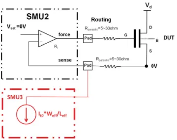
Fig. 9. Configuration of an OP-based SMU and a n-FET for Vtmeasurement
with one force-measure iteration. The target current defined for Vt is forced
as a negative current by an additional SMU.
configuration of the OP in the tester’s SMU. Instead of the conventional unity-gain buffer configuration (e.g., as shown in Fig. 1), the SMU OP is connected as shown in Fig. 9 by separating the force and sense nodes and reconnecting the sense node to the DUT source node. In such a configuration, in contrast to the circuits of Fig. 1, SMU2 is no longer functioning as a unity-gain buffer at the gate terminal. Instead, in the proposed configuration, it is configured as a two stage operation amplifier, i.e., SMU2 plus DUT are connected to form a voltage follower. In addition, as the tester’s SMU op-amp is constructed using discrete ICs, it can easily achieve very high-gain operation while remaining free from sensitivity to process variation. The overall gain of this two stage OP exceeds 100 dB. Therefore, the inverting input node and the noninverting input node can be considered connected by a virtual short. For the Vt measurement, Vset is 0 V, and the
voltage at the source terminal is also forced to almost exactly 0 V because of the following two reasons. First, the op-amp’s gain is high enough to enable the op-amp to effectively maintain the virtual short between the two op-amp input nodes. Second, the current (< 0.1 µA) flowing between sense pad and source node is small enough that the IR drop in this path has negligible impact. Meanwhile, SMU3 functions as the current source, forcing the negative target current used in the constant-current Vt definition, which flows completely through the DUT because of the high input impedance of the op-amp input terminals. Therefore, the output node of the op-amp is able to quickly drive the gate voltage to the correct value of Vt once Vset, Vd, Vb, and the target current for the constant current Vt definition are assigned. Vt can be measured in either the saturation or the linear region by appropriately adjusting Vd. Typically, Vd = Vdd and Vd = 0.05 V are the bias conditions for saturation-mode Vt (Vts) and linear-mode Vt (Vtl), respectively. This configuration
affords several advantages. First, this configuration has high Vt measurement accuracy. The accuracy is better than the binary search approach because there is almost no error in the target current that is forced by a second SMU. The second benefit of
Fig. 10. SMU connections for fast Vt measurement by using the proposed
OP-based SMU.
this OP-based SMU approach is the absence of body effect in
Vt measurement. The third benefit is that multiple additional device parametrics, such as Ion, Ioff, and so forth, can be
measured in this configuration. For the Vt measurement, note that we deliberately avoid connecting the current source to the DUT drain terminal, because a less accurate Vt value would result from connection to the drain because of an extra junction leakage current path that would remove part of the reference current Ids (Vt) = I0, n∗Weff/Leff.
B. Implementation for Stand-Alone DUT
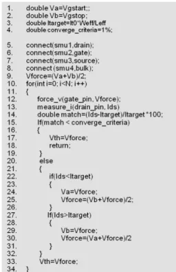
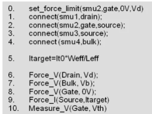
Fig. 10 shows the SMU connections for fast Vt testing using an OP-based SMU. Other than the OP-based SMU2 connected to the gate and source terminals, there are two unity-gain buffers for the drain and bulk terminals, and one current source for the source terminal. SMU2, configured with separated force and sense nodes, is connected to both the gate and source terminals of the DUT. The drain and bulk terminals are connected to SMU1 and SMU4, respectively, and the negative current (i.e., target current) source is provided by SMU3. The body effect issue faced by on-chip OP test structures is completely eliminated in this test configuration. Four SMUs are required for the fast Vt measurement, the same number required by the binary search algorithm. As the OP-based SMU can read out the output voltage of the OP, there is no need for an additional SMU to sense the voltage at the gate terminal as required in the circuit of Fig. 8. Fig. 11 shows the fast Vt algorithm to obtain Vtwith only a single force-measure iteration. Note that the voltages at each terminal must be forced in the sequence shown, i.e., first drain, then bulk, then gate, and lastly the negative current should be forced at the source. If this forcing sequence is not strictly observed, the voltage overshoot might damage or breakdown the DUT.
Fig. 11. Pseudocode of Vt measurement by OP-based SMU.
C. Implementation for Array Test Structure Vt Measurement Although transistor characterization during technology development and manufacture monitoring requires the char-acterization of a number of stand-alone DUTs, because of the increasing importance of LDEs, it is increasingly challenging to adequately characterize a technology with a limited number of stand-alone DUT layouts. The typical width and length (W/L) matrix required for basic SPICE modeling may contain several tens of individual DUTs, but when multiple LDEs such as well-proximity effect and various stress-dependent geometry effects must be characterized, hundreds or even thousands of DUT layouts must be studied. Such studies can be performed on discrete DUTs in a development environment on a test vehicle, but even with the reduction in test time enabled by our proposed method, the area required for such a large number of DUTs renders it unfeasible to monitor a large number of DUTs in a production environment because all test structures must fit within the limited space in the wafer scribe line. This challenge, however, can be addressed by placing multiple DUTs in an compact addressable array and accessing the individual DUTs via a multiplexer and transmission gates. The basic tradeoff between stand-alone DUTs and array-based structures is straightforward. Stand-alone DUTs can be accessed with relatively straightforward measures to address any possible parasitics, and all traditional transistor character-istics can be measured. However, even the most innovative pad sharing techniques can only place approximately 20 DUTs in a typical scribe-line test structure having dimensions approxi-mately 2500× 60 µm, and contacted directly by an automated tester probe card. In contrast array-based structures require substantially more design effort to eliminate parasitics, which may otherwise introduce measurement inaccuracy. Further, some parametrics, such as the very low off-state currents of long channel transistors, may be challenging or impossible to measure in array test structures. With appropriate design of access circuitry, however, array test structures can perform accurate measurements of most key parametrics, such as Idsat, Vtsat, and many other key points on the I –V characteristic, and over a thousand DUTs can easily fit in a single scribe-line test structure. The design measures required to achieve optimal accuracy in array-based test structures, as well as the details of the array-based test structure employed in this paper, were discussed at greater length in [19]. As discussed
Fig. 12. Vt measurement by OP-based SMU in an array test structure.
below, the test time reduction by our proposed test algorithm can be readily combined with array-based test structures to perform characterization of a large number of DUTs, which would otherwise be extremely challenging in a manufacturing environment because of prohibitively long test time. For this research, an addressable array containing multiple transistors with various values of W/L is used for the characterization of
Vt variation.
Fig. 12 shows the proposed transistor array with 16× 64 = 1024 test units. In-depth discussion of the design and opera-tion of the array was discussed in [19], but its funcopera-tion is summarized in brief below. Each test unit consists of a few transmission gates and one DUT (a FET in this example). The DUT can be measured by selecting the corresponding test unit through the column decoder. As shown in Fig. 12, the gate terminals of the FETs in a selected column are connected to SMU2 and the source sense terminals are connected to SMU3, which is fed back to SMU2, while the switches connecting drain, source, gate, and bulk terminals in unselected columns are turned off. Typically, the transmission gates need to be sized large enough to have negligible voltage drop at the current level required for Vt measurement. In this experiment, however, the drain and source terminals of all DUTs are connected to one SMU with force/sense IR drop compensation, respectively. With this voltage compensation mechanism, wide metal routing for the drain and bulk terminals is not required to reduce the parasitic resistance of these connections, allowing a more compact testline layout. The Vt of the selected DUT is read out by SMU2. In addition, all periphery circuits, such as latches and decoders, are designed with 2.5-V I/O devices so that their background leakage current, including subthreshold leakage current and gate oxide leakage current, can be reduced, and their performance will not be affected by any process variation that may be present in the advanced process under research.
IV. EXPERIMENTALRESULTS A. Binary Search Vt Testing Time
The time required for a single binary search force-measure iteration consists mainly of contributions from two stages in
Fig. 13. Time trace of successive iterations for Vtmeasurement by binary
search, showing gate voltage (left axis) and measured current matching percentage (right axis). Id is the measured current at the drain node and
It is the target current for Vt definition by the constant current criteria.
the execution of the algorithm: 1) the forcing of the voltage and 2) the current measurement. The time required to force a voltage is principally a function of the SMU settling time, which is relatively short, typically∼100 µs. The time required for current measurement is determined by the current level to be measured and the sample size, which is defined by the inte-gration time. This second contribution is strongly dependent on the magnitude of the target current if the integration time is set to the same value. For measurement of a lower current level, the SMU requires a longer measurement time because it must switch from the measurement mode for a higher current to that of a lower current. Typically, the time required for changing the current range a few ms because it requires the switching of electromechanical components in the tester.
In this experiment, it is determined to require approxi-mately 7 and 30 ms for one force-measure iteration at the microampere and nanoampere current levels, respectively. As discussed in Section II-A, Vt is defined by the gate voltage resulting in the measured drain current matching the target current I 0∗Weff/Leff within a specified criteria, for instance 1%, which introduces about 0.5 mV error based on SPICE simulation. Fig. 13 (curve A) plots the gate voltage (Vg) versus iteration number throughout the successive force-measurement cycles of a Vt measurement by binary search. During the course of the measurement, Vg is set successively to values above and below Vt, approaching Vt with an increasingly tight tolerance, and converging when the drain current Id (measured by SMU1 in the connection scheme of Fig. 2) approximately matches the target current. Curve B plots the percent mismatch between the measured drain current and the target current, showing that typically nine or ten iterations are required to reach the 1% matching criteria.
To obtain representative Vt measurement times for the binary search algorithm, transistors of two different channel lengths are evaluated. Transistor A is a longer channel device with a target current in the nA range. Transistor B is a short channel device with a target current of order 1µA. Table I lists the device characteristics and Vt testing times obtained using the binary search algorithm. The shorter channel transistor with microampere target current requires approximately 69 ms,
Average of testing time 270.06 ms 68.75 ms Standard. dev of testing time 8.98 ms 20.83 ms
Iteration number 8–10 6–9
whereas the longer channel transistor requires a testing time of approximately 270 ms. The number of iterations required for measurement of the longer channel transistor is slightly higher than for the shorter channel transistor because of the inevitable noise increase from lower target current to be measured. Moreover, the testing time for the lower target current significantly increases by nearly 4× because of the additional time required for the SMU range to switch in order to accommodate the lower current level.
B. Vt Testing Time Improvement Using the Interpolation
Method
According to the analysis in Section II-B, the Vt testing time using the interpolation method can be reduced to 60 and 14 ms for transistors A and B, respectively, because the interpolation method requires only two force-measure iteration cycles, compared with approximately 6–9 cycles for binary search.
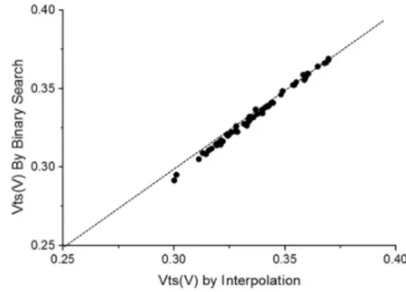
Fig. 14 shows a scatter plot of Vt obtained from the binary search and interpolation methodologies for devices fabricated using an advanced process technology. Evidently the data obtained from these two methods exhibit excellent linearity even though the number of force-measure iterations is reduced to two by using the interpolation algorithm. In other words, the interpolation algorithm shows no degradation in the accuracy of the Vt measurement, but has a shorter testing time. As discussed in the previous section, the interpolation methodology is, however, only suitable for characterization of nearly identical transistor sizes having very similar target current values, and furthermore, these transistors must have no double hump or similar nonlinearities in their Id–Vg characteristics.
C. Simulation of Vt Measurement Using OP-Based SMU The configuration of Fig. 9 is verified by HSPICE simula-tions in an advanced process technology. In this simulation, a stand-alone DUT (nMOS) is directly connected to a high-gain op-amp with gain of approximately 100 dB. The bias condition of the gate, source, and bulk terminals is set as shown in Fig. 10 to emulate the test condition. To trace the voltage modulation at the gate terminal, the drain voltage is, however, swept from 0 V to Vdd rather than a fixed bias of 0.05 V
or Vdd for Vtl or Vtsmeasurement. With the high-gain OP, the
Fig. 14. Scatter plot of Vtsmeasurements by the binary search versus the
interpolation method.
Fig. 15. Simulation of Vtmeasurement by an OP-based test structure. Plotted
data are (a) OP output voltage, i.e., Vt and (b) DUT source voltage, which is
clamped at 0 V because of virtual short to Vset.
voltage of the source terminal is clamped at 0 V by the virtual short with the OP noninverting input. Therefore, the absence of body effect in the Vt measurement in this configuration can be verified in simulation if the bulk terminal is also biased at 0 V. As plotted in Fig. 15, curve (a) shows that the voltage at the output node of the OP, i.e., Vt, is well modulated by a 10 mV change in the drain voltage. Curve (b), which represents the voltage at the source terminal, remains at 0 V for all values of the drain voltage, indicating that the inverting and noninverting inputs of the OP amp are a strong virtual short because the gain of the op-amp is sufficiently large. Therefore, by definition, the Vt in the saturation and linear regions can be measured by forcing Vd = 0.05 and Vd = Vdd respectively, with no
inaccuracy introduced by body effect.
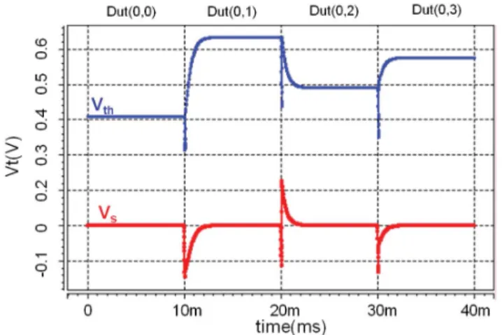
The transient simulation for the validation of this array-based test structure is also checked. Fig. 16 shows the simulation waveform of DUT(0, 0)− DUT(0, 3) in the array-based test structure shown in Fig. 12. The voltage-modulated output signal is repeated periodically as the macro scans through the 1024 devices in the array, modulated by the clock period for address switching. These simulations demonstrate the repeatability of successive measurements and the time
Fig. 16. Transient simulation of OP-based Vtmeasurement in an array-based
test structure. Traces for the measurement of four DUTs are shown, where each DUT has a different threshold voltage.
stability of voltage levels between transitions. As indicated by the voltage trace of Fig. 12, although the specific Vt values of each of the four DUTs (DUT(0, 0)− DUT(0, 3)) are different, nearly identical settling time is achieved in each case. This indicates that the OP-based SMU can settle within a clock period of 2–3 ms with 1 pF parasitic capacitance.
This settling time does constitute a limitation to the speed of the OP-based measurement, but even with this settling time, because only a single iteration is required for convergence, the
Vt measurement demonstrated here is a factor of∼ 10 faster than that of the binary search algorithm (which requires∼10 iterations to converge), and a factor of ∼ 2 faster than the interpolation method (which requires two iterations).
D. Stand-Alone DUT Test Result
The proposed OP-based Vt measurement method introduced in Section III-B delivers significant improvement in testing time and measurement accuracy. To demonstrate this, in this experiment, the measurement time and accuracy is evaluated for one of the DUTs fabricated using an advanced process technology. The Vt measurement by the proposed methodol-ogy is repeated 1000 times using an Agilent parametric tester to ensure the statistical significance of the result. As shown by the histogram in Fig. 17, the Vt value obtained by the OP-based methodology has a very small measurement error that can contribute to better measurement accuracy.
The standard deviation of the 1000 Vt measurements is approximately 0.15 mV, much smaller than the 0.5 mV error resulting from the 1% current matching criteria discussed in Section IV-A. In addition, the test time is significantly reduced from∼ten force-measure iterations to one, i.e., from ∼60 to ∼6 ms for the short-channel transistor A of Table I, which is expected based on the discussion in Section III-A. The major reason for this improvement in testing time is the use of only a single force-measure iteration. Improved measurement accuracy is further ensured by precise setting of the target current and the absence of impact of imperfections and variability of an on-chip OP design, which may occur in an on-chip OP approach such as [23].
Fig. 17. Vtdistribution obtained by 1000 repeated measurements on the same
DUT (shorter channel transistor) by OP-based measurement of the array test structure.
E. Array-Based Test Structure Result
The test speed improvement of OP-based Vt measurement is most significant in array-based test structures. In addition, to the test time savings from reducing ∼10 force-measure iterations to one, the array-based test structure avoids the time required for the connect and disconnect operations between SMUs and testline I/O pads for measurement of successive DUTs that must be performed before the force-measure iter-ations can begin. Typically, the time required for connect and disconnect operations, which are performed by mechanical switches, is about 1 ms. The time required for changing and latching addresses for DUT selection in array-based test structures is, however, less than 1 µs that is much faster than the connect and disconnect mechanical operations. In practice, for array-based test structure measurement, connec-tion between SMU and pad is performed at the first address and disconnection is performed at the last address because the same SMUs are used for the force and sense terminals of all DUTs. Moreover, the testing time overhead can be further improved in array-based test structure by elimination of prober index time. In general, the prober index time is typically a few hundred ms if the required prober chuck displacement is less than 1 mm. In this experiment, a test time comparison is performed between (A) nonarray-based test structures and (B) array-based test structure. Both cases include∼1 k DUTs with different W/L combinations. In case (A), nonarray test structures, however, required more a larger number of testlines and thus more layout area. Typically, only eight DUTs can be placed in one nonarray testline due the constraint that DUTs must not have excessive sharing of I/O pads. Therefore, 1 k DUTs requires 1000/8 = 125 testlines in case (A). The Vt of each DUT is measured by the proposed methodology under two different test conditions: 1) nonarray DUTs in case A, which require a SMU connect and disconnect for each individual DUT and 2) an array-based test structure in case (B), which only requires a connect and disconnect operation of the first and last addresses, respectively. As shown in Table II, the time required specifically for the ∼1 k DUT
and (B). However, case (A) it requires additional overhead of 1000 ms from SMU connect and disconnect operations. Moreover, case A utilizes 125 probe card touch downs instead of the single touch down of case (B). Therefore, case (A) requires 125 prober chuck displacements during measurement. Assuming a prober index time of 200 µs, case (A) incurs an additional penalty of approximately 125×200 ms are required for case (A). Therefore, the total test time is approximately 32 000 and 6002 ms for the proposed Vt measurement on nonarray and array-based test structures, respectively. The test speed is further improved by factor of 5× by taking advantage of a single connect/disconnect and elimination of the prober index time during measurement of the array-based test structure.
V. CONCLUSION
In this paper, we successfully developed a fast Vt testing methodology using an OP-based SMU to dramatically improve the test time required for Vt measurement. Using the proposed techniques, the Vt testing speed can improved by a factor of 5–10 relative to the binary search algorithm (the algorithm most commonly used in the authors’ experience), and by a factor of∼2 relative to the interpolation algorithm, with accu-racy better than 0.15 mV (compared with∼0.5 mV typically achieved by the binary search or interpolation algorithms). In addition, combined with a array-based test structure design including ∼1 k individually addressable FETs, the test time of Vt measurements can be further improved by a factor of 5× because of elimination of overhead due to multiple tester connect and disconnect operations and prober index times. A series of experiments were conducted on both mature and newly developed process technologies to validate the effectiveness and the superiority of the overall proposed test structure and its application.
REFERENCES
[1] K. Bernstein, S. R. Nassif, D. J. Frank, A. E. Gattiker, W. Haensch, B. L. Ji, E. J. Nowak, D. J. Pearson, and N. J. Rohrer, “High-performance CMOS variability in the 65-nm regime and beyond,” IBM J. Res.
Develop., vol. 50, no. 4–5, pp. 433–449, Jul. 2006.
[2] M. Kanno, A. Shibuya, M. Matsumura, K. Tamura, H. Tsuno, S. Mori, Y. Fukuzaki, T. Gocho, H. Ansai, and N. Nagashima, “Empirical characteristics and extraction of overall variations for 65-nm MOSFETs and beyond,” in Proc. IEEE Symp. VLSI Technol., Jun. 2007, pp. 88–89. [3] M. Orshansky, S. R. Nassif, and D. Boning, Design for
Manufactura-bility and Statistical Design, A Constructive Approach. New York, NY,
USA: Springer-Verlag, Dec. 2007.
[4] B. Stine, D. Boning, and J. Chung, “Analysis and decomposition of spatial variation in integrated circuit processes and devices,” IEEE Trans.
Semicond. Manuf., vol. 10, no. 1, pp. 24–41, Feb. 1997.
[8] S.-H. Lee, D.-Y. Lee, T.-J. Kwon, J.-H. Lee, and Y.-K. Park, “An efficient statistical model using electrical tests for GHz CMOS devices,” in Proc.
5th Int. Workshop Stat. Metrol., 2000, pp. 72–75.
[9] K. Nagase, S.-I. Ohkawa, M. Aoki, and H. Masuda, “Variation status in l00 nm CMOS process and below,” in Proc. IEEE Int. Conf.
Microelectron. Test Struct., vol. 17. Mar. 2004, pp. 257–261.
[10] T. Ghani, M. Armstrong, C. Auth, M. Bost, P. Charvat, G. Glass, T. Hoffmann, K. Johnson, C. Kenyon, J. Klaus, B. McIntyre, K. Mistry, A. Murthy, J. Sandford, M. Silberstein, S. Sivakumar, P. Smith, K. Zawadzki, S. Thompson, and M. Bohr, “A 90 nm high volume manufacturing logic technology featuring novel 45 nm gate length strained silicon CMOS transistors,” in IEEE IEDM Tech. Dig., Dec. 2003, pp. 11.6.1–11.6.3.
[11] C.-H. Chen, T. L. Lee, T. H. Hou, C. L. Chen, C. C. Chen, J. W. Hsu, K. L. Cheng, Y. H. Chiu, H. J. Tao, Y. Jin, C. H. Diaz, S. C. Chen, and M. S. Liang, “Stress memorization technique (SMT) by selec-tively nitride capping for sub-65nm high-performance strained-Si device application,” in Symp. VLSI Technol. Dig. Tech. Papers, Jun. 2004, pp. 56–57.
[12] H. Tsuno, K. Anzai, M. Matsumura, S. Minami, A. Honjo, H. Koike, Y. Hiura, A. Takeo, W. Fu, Y. Fukuzaki, M. Kanno, H. Ansai, and N. Nagashima, “Advanced analysis and modeling of MOSFET char-acteristic fluctuation caused by layout variation,” in Proc. Symp. VLSI
Technol., Jun. 2007, pp. 204–205.
[13] K. Agarwal, F. Liu, C. McDowell, S. Nassif, K. Nowka, M. Palmer, D. Acharyya, and J. Plusquellic, “A test structure for characterizing local device mismatches,” in Symp. VLSI Circuits Dig. Tech. Papers, 2006, pp. 67–68.
[14] Y. Z. Xu, C. S. Chen, and J. I. Watt, “Investigation of 65 nm CMOS transistor local variation using a FET array,” Solid State Electron., vol. 52, no. 8, pp. 1244–1248, Aug. 2008.
[15] C. Jakubiec and R. Lefferts, “An integrated test chip for the complete characterization and monitoring of a 0.25 µm CMOS technology that fits into scribe line structures 150µm by 5,000 µm,” in Proc. Int. Conf.
Microelectron. Test Struct., Mar. 2003, pp. 59–63.
[16] N. Izumi, H. Ozaki, Y. Nakagawa, N. Kasai, and T. Arikado, “Evaluation of transistor property variations within chips on 300-mm wafers using a new MOSFET array test structure,” IEEE Trans. Semicond. Manuf., vol. 17, no. 3, pp. 248–254, Aug. 2004.
[17] K. Agarwal, J. Hayes, and S. Nassif, “Fast characterization of threshold voltage fluctuation in MOS devices,” IEEE Trans. Semicond. Manuf., vol. 21, no. 4, pp. 526–533, Nov. 2008.
[18] K. Doong, T. J. Bordelon, L.-J. Hung, C.-C. Liao, S.-C. Lin, S. P.-S. Ho, S. Hsieh, and K. L. Young, “Field-configurable test structure array (FC-TSA): Enabling design for monitor, model, and manufacturability,” IEEE
Trans. Semicond. Manuf., vol. 21, no. 2, pp. 169–179, May 2008.
[19] T.-C. Luo, M. C.-T. Chao, M. S.-Y. Wu, K.-T. Li, C. C. Hsia, H.-C. Tseng, P. A. Fisher, C.-U. Huang, Y.-Y. Chang, S. C. Pan, and K. K.-L. Young, “A novel array-based test methodology for local process variation monitoring,” in Proc. Int. Test Conf., Nov. 2009, pp. 1–9. [20] J. A. Croon, H. P. Tuinhout, R. Difrenza, J. Knol, A. J. Moonen,
S. Decoutere, H. E. Maes, and W. Sansen, “A comparison of extraction techniques for threshold voltage mismatch,” in Proc. Int. Conf.
Micro-electron. Test Struct., Apr. 2002, pp. 235–240.
[21] H. Lee, S. Oh, and G. Fuller, “A simple and accurate method to measure the threshold voltage of an enhancement-mode MOSFET,” IEEE Trans.
Electron Devices, vol. 29, no. 2, pp. 346–348, Feb. 1982.
[22] S. Wolf, Silicon Processing for the VLSI Era Volume 3: The Submicron
MOSFET. San Jose, CA, USA: Lattice Press, Oct. 1994.
[23] B. L. Ji, D. J. Pearson, I. Lauer, F. Stellari, D. J. Frank, L. Chang, and M. B. Ketchen, “Operational amplifier based test structure for quan-tifying transistor threshold voltage variation,” IEEE Trans. Semicond.
Manuf., vol. 22, no. 1, pp. 51–58, Feb. 2009.
[24] Y. Taur and T. H. Ning, Fundamentals of Modern VLSI Devices, 2nd ed. Cambridge, U.K.: Cambridge Univ. Press, Aug. 2009.
[25] M. H. Na, E. J. Nowak, W. Haesch, and J. Cai, “The effective drive current in CMOS invertors,” in Proc. IEDM, Dec. 2002, pp. 1–4. [26] S.-D. Kim, S. Narasimha, and K. Rim, “An integrated methodology for
accurate extraction of S/D series resistance components in nanoscale MOSFETs,” in IEEE IEDM Tech. Dig., Dec. 2005, pp. 149–152.
Tseng-Chin Luo received the M.S. degree in
mate-rial science and engineering and the Ph.D. degree in electrical engineering from National Chiao-Tung University, Hsinchu, Taiwan, in 1994 and 2012, respectively.
He joined Winbond Electronics, Hsinchu, in 1996, and then transferred to Worldwide Semiconductor Manufacturing Corporation, Hsinchu, in 1997. His major focus was parametric testing and process integration. Since 1998, he has been developing processes for 0.18 and 0.13µm technology with the Logic Technology Research and Development Division, Taiwan Semiconduc-tor Manufacturing Corporation (TSMC), Hsinchu. He focused on developing test structures and fast test methodology for process characterization, design manufacturing and yield optimization, establishing infrastructure to improve design effectiveness and analysis quality. He is currently a Project Manager with Fast Parametric Test Solutions, TSMC.
Mango C.-T. Chao received the B.S. and M.S.
degrees from the Department of Computer and Information Science, National Chiao-Tung Univer-sity, Hsinchu, Taiwan, in 1998 and 2000, respec-tively, and the Ph.D. degree from the Department of Electrical and Computer Engineering, University of California, Santa Barbara, CA, USA, in 2006.
He joined the Department of Electronics Engineer-ing, National Chiao-Tung University, where he is currently an Assistant Professor. His current research interests include memory testing, on-chip test com-pression/decompression, WAT test-structure design, power-related testing, and physical design automation.
Huan-Chi Tseng was born in Hsinchu, Taiwan, in
1964. He received the B.S. and M.S. degrees from the Material Science and Engineering Department, National Tsing Hua University, Hsinchu, in 1986 and 1991, respectively.
He was with Winbond Electronic Corporation, Hsinchu, in 1992, as a Process Integration Engineer and joined Taiwan Semiconductor Manufacturing Corporation, Hsinchu, in 1993. From 1993 to 1998, he worked in the memory technology area as a Process Integration Engineer for 0.8µm-EPROM,
0.5µm-EPROM, 0.5 µm DRAM, and 0.45 µm DRAM. He became a Section
Manager and led the integration team that implemented Fujitsu’s 0.22 µm DRAM technology in TSMC fab lines in 1998. In 1998, he served as a Section Manager of defectivity and supervised the defect technical board. After 1999, he worked on CMOS logic process integration. He joined TSMC’s 300 mm pilot line as an Integration Manager in 2000 and helped to establish the first 0.13 µm CMOS technology in the F12 300 mm fab line. Since 2003, he has been with the Product Engineering Division as an Advance Product Engineering Department Manager. He collaborated with Research and Development teams to establish C011, N90, N80, N65, N55, N45, N40, N32, and N28 technologies and his team is responsible for advance technology EFA/PFA yield enhancement, DRM, DFM and process window characterization. He is currently the Deputy Director of the New Technology Product Engineering Division, TSMC.
Masaharu Goto was born in 1962. He received the
B.S. degree in electrical and electronic engineering from the Tokyo Institute of Technology, Tokyo, Japan, in 1985.
He is a Project Manager in the Semiconductor Parametric Test Research and Development Depart-ment of Agilent Technologies, Tokyo. In 1985, he joined Yokogawa-Hewlett-Packard, which sub-sequently became Agilent Technologies Japan. He has been responsible for multiple aspects of product and technology development for a wide portfolio semiconductor measurement products.
Philip A. Fisher received the B.S. degree in physics
from the University of Washington, Seattle, WA, USA, in 1991, and the M.A. and Ph.D. degrees in physics from Harvard University, Cambridge, MA, USA, in 1994 and 1999, respectively.
He performed research on the development of a thermoelectric micro-refrigerator based on supercon-ducting tunnel junctions, which was reviewed in The
Economist, March 21, 1998. From 1999 to 2000,
he was a Foundry Process Support Engineer with Analog Devices Corporation. From 2000 to 2008, he was engaged in process integration and advanced SOI transistor development with Advanced Micro Devices Corporation, during which time he advanced from a Senior Integration Engineer to a Senior Member of Technical Staff in recognition of his contributions to the transistor development for the 130, 90, 65, 45, and 32 nm technologies. Since 2008, he has been a Manager with the Advanced Device Technology Department, Taiwan Semiconductor Manu-facturing Corporation, Hsinchu, where his work has focused on development and characterization of high performance and low power transistors. He is the author or co-author of 27 peer reviewed publications and 27 U.S. patents.
Yuan-Yao Chang was born in Pingtung, Taiwan,
in 1982. He received the B.S. degree from National Chiao-Tung University, Hsinchu, Taiwan, in 2004, and the M.S. degree in microelectromechanical sys-tem engineering from National Tsing-Hua Univer-sity, Hsinchu, in 2006.
He joined Taiwan Semiconductor Manufacturing Corporation, Hsinchu, in 2006, and he is currently a Senior Engineer with the Advanced Technology Infrastructure Program, where he is engaged in the design of test structures for advanced process characterization.
Chi-Min Chang received the B.S. degree from
the Department of Electrical Engineering, National Central University, Taoyuan, Taiwan, in 2006, and the M.S. degree from the Department of Electron-ics Engineering, National Chiao-Tung University, Hsinchu, Taiwan, in 2008.
He is currently with Taiwan Semiconductor Man-ufacturing Company, Hsinchu, where he focuses on test structure design and WAT testing.
system.
Katsuhito Iwasaki was born in Hyogo, Japan, in
1974. He received the B.S. and M.S. degrees in electrical engineering from Osaka University, Osaka, Japan, in 1996 and 1998, respectively.
He joined Agilent Technologies International Japan, Ltd., Tokyo, Japan, in 2001, where he is a Research and Development Engineer with Para-metric Test Business, Hachioji Semiconductor Test Division.
![Fig. 12 shows the proposed transistor array with 16 × 64 = 1024 test units. In-depth discussion of the design and opera-tion of the array was discussed in [19], but its funcopera-tion is summarized in brief below](https://thumb-ap.123doks.com/thumbv2/9libinfo/7628353.134202/7.918.75.447.77.346/proposed-transistor-array-discussion-design-discussed-funcopera-summarized.webp)