I667
IEEE TRANSACTIONS ON ELF.Cl.KON DEVICES. VOL. 37. N O . 7. JULY 1990
An Analytic Saturation Model for Drain and Substrate
Currents of Conventional and LDD MOSFET’s
Absfracf-An analytic saturation model for conventional and LDD MOSFET’s is developed by using the pseudo-two-dimensional approx- imation (PTDA) in the channel and drain regions to obtain both the channel length modulation factor and the maximum electric field. Using the established I-V model in the linear region, the drain currents of conventional and LDD MOSFET’s can be explicitly calculated. Fur- thermore, the substrate currents of conventionallLDD MOSFET’s are calculated by using an existing simplified substrate current formula and the developed maximum electric field model. Using a two-dimen- sional numerical MOS device simulator, it is shown that the accuracy of the developed maximum electric field model is acceptable for cal- culating the substrate currents of conventionallLDD MOSFET’s. Moreover, the parameters used in the developed model can be deter- mined by the existing extraction methods and the developed optimi- zation technique. Comparing the calculated drain and substrate cur- rents with the experimental data measured from the test transistors with conventionallLDD MOS structures, the developed saturation model is shown to be valid for a wide range of channel lengths and bias conditions.
NOMENCLATURE
External gate (drain) to source Substrate bias.
Intrinsic drain (source) voltage. Intrinsic gate-source voltage. Intrinsic drain-source voltage. Saturation drain-source voltage in Drain current.
Drain current at the onset of satu- Substrate current.
Parasitic resistance of the drain (source).
Resistance of the lightly doped re- gion near the drain (source) side of LDD MOS devices.
voltage.
the channel region.
ration condition.
Effective channel length (width). Channel length modulation factor
in the channel (drain or n - ) re- gion.
Manuscript received December 3 , 1989; revised February 1, 1990. This work was supported by the National Science Council, Republic of China. under a special fund. The review of this paper was arranged by Associate Editor P. K. KO.
The authors are with the Institute of Electronics. National Chiao-Tung University, Hsin-Chu, Taiwan, Republic of China.
IEEE Log Number 9035759.
vTO
VFB
4s.
invEm,,
Oxide thickness (capacitance per unit area).
Dielectric permittivity of silicon (oxide).
Maximum electron mobility in the inversion layer of the active channel device.
Threshold voltage at zero drain bias.
Flat-band voltage of the active channel device.
Surface potential at strong inver- sion condition.
Electric potential in PTDA sec- tion.
Empirical constants for electron mobility in the inversion layer of the active channel device. Critical electric field. Saturation velocity.
Flowing path depth of the drain current in PTDA section near the channel side.
Flowing path depth of the drain current at the pinch-off point. Depletion width in PTDA section
near the channel side.
Depletion width in GCA section. Doping profile in the channel re- Mobile charge density.
Junction depth of the drain (lightly Depletion width under the drain re- Doping concentration in the drain Empirical constants for the sub- Maximum electric field in PTDA
gion.
doped) region. gion.
(lightly doped) region. strate current.
section.
I . INTRODUCTION
HEN the electric field near the drain side reaches the critical field for saturation velocity, a short- channel MOSFET will operate in the saturation region. 00 18-9383/90/0700- 1667$01
.OO
0
1990 IEEE1668 1EF.F. 'TRANSACTIONS ON ELECTRON DEVICES. VOL 27. NO. 7. JULY IY90 Furthermore, the high electric field in the drain junction
may result in carrier impact ionization and produces the substrate current. On the other hand, the pinch-off point of the inversion channel may move toward the source side as the drain bias increases, resulting in the rise-up of the drain current. In order to analyze the high-field effects of a short-channel MOSFET, a so-called pseudo-two-di- mensional approximation, which can obtain the analytic expression, has been proposed by El-Mansy et a l . [ l ] .
' Based on this approximation, KO er al. [2] have proposed an unified model to characterize both the drain and sub- strate currents. Later on, this model has been further mod- ified by using the empirical equation [3] in order to im- prove the existing deficiency. However, this model is valid only for the case of the uniformly doped substrate, which is not realistic for the currently fabricated MOS devices. Recently, Tanaka et a l . [4], based on the same approach, have also proposed a self-consistent model by involving very complicated iterations in order to calculate the currents directly. However, both models mentioned above do not show wide-range validity for different biases and channel lengths. More recently, Mayaram et a l . [5]
have proposed a model for LDD MOSFET's, in which the electric field and the channel length modulation factor have been calculated by assuming the uniformly doped substrate. However, the channel length modulation factor is found not to be equal to zero at the onset of saturation condition. This deficiency will cause the discontinuity of the drain current at the transition between the linear and saturation regions.
In this paper, an analytic saturation model for conven- tional/LDD MOSFET's is presented. The major advan- tage of the proposed model is that the drain and substrate currents of ConventionaULDD MOSFET's can be analyt- ical calculated from the external voltages without any it-
sensitive to the maximum electric field in the drain junc- tion, a two-dimensional numerical MOS device simulator is used to verify the calculated maximum electric field. In Section 111, the fabrication data of the fabricated conven- tional/LDD MOSFET's and the methods to extract the parameters for calculating the drain and substrate currents are described. In Section IV, the calculated drain and sub- strate currents are compared with the experimental data measured from the fabricated conventional/LDD MOS- FET's. It is shown that good agreement between the de- veloped model and the experimental results has been ob- tained for a wide range of biases and channel lengths by using a set of parameters, and the calculated drain current is continuous at the transition between the linear and sat- uration regions. In Section V, conclusions are given.
11. THE SATURATION MODEL
When a MOSFET is operated in the saturation region, the channel region can be divided into two sections, as shown in Fig. l(a). One is called the gradual-channel- approximation (GCA) section, where the channel electric field is less than the critical field; the other is called the pseudo-two-dimensional-approximation (PTDA) section, where the electric field exceeds the critical field and car- riers move with the saturation velocity.
A , The Gradual-Channel-Approximation Section
In this section, it is assumed that impact ionization can be neglected. This assumption is similar to that used in the channel region where the gradual-channel approxi- mation is valid. Therefore, the drain current in the satu- ration region can be calculated from the formulas derived for the linear region with slight modifications. Based on our previously published model [6]-[9], the drain current in the linear region can be written as
where erations. This property is very important for applications
in circuit analysis. In Section 11, the pseudo-two-dimen- sional approximation is applied to the channel and drain regions of conventional/LDD MOS structures to obtain both the channel length modulation factor and the maxi- mum electric field. Based on the well-established I - I /
model for the linear region published in [6]-[9] and using the calculated channel length modulation factor, the drain current in the saturation region can be easily calculated. Using a simplified expression for the substrate current proposed by Chan er al. [ 101 and the calculated maximum electric field, the substrate current can be easily obtained. Since the simplified substrate current expression is very
and
as shown in Fig. l(b); a = - k , b =
$
+
k , and k is the slope of the threshold voltage with respect to V,, at zero drain bias. The parameters used above have been de- fined in [6]-[9], which can be easily determined by a se- ries of extraction techniques.Substituting L and V(l,,s, with L - ALI and V,/,,t, re- spectively, the drain current in the saturation region can
I669
HUANG A N D WU: SATURATION MODEL FOR DRAIN A N D SUBSTRATE CURRENTS OF MOSFET'S
WAIN
P
B.
The Pseudo-Two-Dimensional-Approximation SectionIn order to consider the two-dimensional effects in the drain region and apply the developed model to LDD MOS
devices, the PTDA method is used in both channel and drain regions. It is assumed that the channel current in this section is uniformly distributed with the finite depths of
do and Rj for the channel and drain edges, respectively. By applying Gauss' law to the rectangular boxes labeled
(1)-(4) for both regions as shown in Fig. l(a), we obtain the following equation for the channel region:
do
=
-3
s'
s
N ( y ) d y d rEsi -ALI 0
Fig. 1. (a) The schematic diagram of a MOSFET operated in the saturation region. (b) Equivalent circuit of a MOSFET.
( 7 )
Q,,,
-s'
- d r .- A L I Esi
be written as
where A L , is the channel length modulation factor in the channel region, which can be calculated directly from the terminal voltages and will be given in Section 11-B; Vd,at is the saturation voltage in the channel region, which can zero.
Similarly, the equation in the drain region can be writ- ten as
ALz
be obtained from equations in [6] by setting R,, equal to d 6 Cnx
R
'
-
-1
-[vg,'
-
vFB-
@s.inv -dr
r E,,Using
Vgy,
= V g ,-
Id,R, and (2), Id\ can be solved as[61
dr
-
EcR, ( 3 )-B,
+
( B : - 4 A l C l ) " 2 2A I 1d.T = whereFrom (7) and (8), the differential equations for the po- tential distribution in both regions can be written as (see
01 C O X
B I = 1
+
-[
v g s+
v m-
2 ( v F B+
6s.inv)
-
bvdsat] Appendixes I, 11) 2Esiand
c,
= ~~ v g \ - vm - avdsat)vdsat. ( 6 )L - ALI
2
-
= -Oi(Gz+
V,,,,,), 0 5 x 5 AL2It is noted that the drain current can be directly calcu-
1670 IEEE TRANSACTIONS ON ELECTRON DEVICES. VOL. 37. NO 7. JULY I990
where
1
+
S B )+
SCand Using Qh = G2
+
- GI - V,,,, and the boundaryconditions in (17), we obtain the following quadratic
[ S B - NdR,] -
(
VKc, -vFB
- &,,) equation: (see Appendix 111)A2[
Q,I
~ X P ( ~ I A L I )+
QI,I ~ X P ( - 8 1 4)I2
( 1 4 )+
&[Q,I
exP ( ~ I A L I ) f Qhi exP ( - ~ I A L I ) ]Note that SA, SB, and SC are defined in Appendix I and are explicitly calculated for a MOSFET with double- channel-boron implantations by using the step-profile ap- proximation [7]; is the drain current at the onset of saturation condition; and V g c , and V,I,\, can be simply ex- pressed as
Vg,, = Vgr - Id\‘&
VdY = VdS - k / \ ‘ i t ( R
+
R d ) .( 1 5 )
(
16) Using the following boundary conditions:Equation (28) can be further rewritten as
Q U I exp (elAL1)’ -
41
exp ( ~ I A L I )+ Qhl
= 0. ( 2 9 )Solving (29), exp (BIALI) can be written as
5%
d441x=o-
= L o +I
r = O - =ZLo+
= 4 1 2 . ( 3 0 ) A,,I+
(Ail - ~ Q , I Q ~ I ) I ” 2Q ,
I exp (OIALI) =Therefore, ALl can be expressed by
4
lr+
= V d V41
= E , (17)dr
r = A L z(31
1
the differential equatons in (9) and (10) can be solved and
written as 61
ALI = 3.
1
H U A N G A N D W U : S A T U R A T I O N MODEL FOR D R A I N A N D SUBSTRATE C U R R E N T S O F MOSFET'S 1671 Parameters
&
\I
t,,,(R) N , , s ( c m - 3 ) N , , , , ( c ~ - ~ ) N A B ( C m - 3 ) Y B ( l t m ) W b ( p m ) vpo( v ) conventionalI
2 5 0 3 . 8 0 ~ 1 0 ~ ~ 8 . 0 7 ~ 1 0 ~ ~ 3 . 9 7 ~ 1 0 ' ~ 0 . 1 8 0 . 5 4 -0.60 R, , rn(lm) N d . Nn( ~ m - ~ ) 0 . 3 3 1 . 8 ~ 1 0 ~ ~ration condition and is independent of A L ,
.
Therefore, G I in (13) and G2 in (14) can be easily calculated from the terminal voltages. Moreover,e,,,,
e,,,,
Qn7, Q h 2 , andQ,,
are expressed in terms of GI and G2. so A I l I in (28) can be obtained from the terminal voltages. Therefore, it is eas- ily seen that A L I in (31) can be calculated from the ter- minal voltages without any iterations. Similarly, the same conclusion can be given to A L z in (33). Besides, A L , andAL2 are equal to zero at the onset of saturation condition,
the drain current is therefore continuous at the transition between the linear and saturation regions.
C. The Substrate Current
In order to obtain the analytic form for the substrate current, a simplified substrate current expression pro- posed in [l o ] is used and expressed as
~ , ( C r n - ~ / V - . s ) = ( u n / v ) v ( l / V )
Parameters nos structures\
Conventional 6 7 1 . 4 6 1 . 7 6 ~ 1 0 - ~ 5 . 9 4 ~ 1 0 - ~
LDD 6 0 4 . 8 8 1 . 1 8 ~ 1 0 - ~ 5 . 0 4 ~ 1 0 - ~
where Zd,, can be obtained by (3); A. and Bo are the fitting parameters, which can be determined by the least square method; E,,, is the maximum electric field and can be expressed as
B ( m / v ) R S , R d ( n ) 4 . 8 3 x 1 0 - ' 1 1 . 2 7 5 . 2 2 ~ 1 0 - ~ 1 1 . 2 7
( 3 5 ) in which
e,,
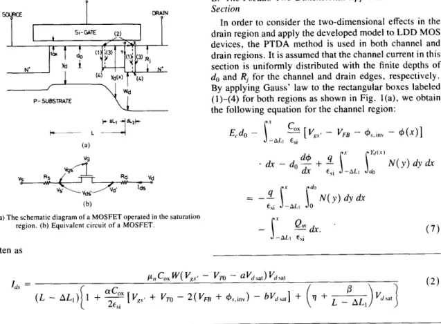
E l , and F I can be calculated by ( 1 I ) , (20), and (21), respectively.From (34), it is clearly seen that the accuracy of E,,, in (35) is extremely important for calculating the substrate current. Using the parameters listed in Tables I and 11, Fig. 2(a) shows a comparison of the calculated E,,, be- tween the developed analytic model in (35) and the nu- merical simulation for different external drain/gate biases and gate oxide thicknesses.' It is shown that the accuracy of the calculated maximum electric field using (35) for conventional MOSFET's is acceptable.
D.
Applications to L D D MOSFETSFor LDD MOS devices, the electric field distribution in the lightly doped n- region becomes very complicated, depending on the doping concentration in the n- region and its overlap with respect to the gate. However, if the maximum electric field occurs at the channel-n- junction in the drain side and the channel length modulation factor in the n - region does not exceed the gate edge, the de- 'The numerical analysis presented in the text was accomplished by an efficient 2-D MOS simulator called SUMMOS (&bmicrometer
m),
which has been developed by the Advanced Semiconductor Device and Technology Research Division, National Chiao-Tung University, Taiwan, Republic of China.veloped model can be easily extended to the LDD MOS devices with slight modifications. The major modifica- tions are that R,, N,,, R,, and R,, in the above derived for- mulas are replaced by r,,, N I , , R ,
+
R,,, and R,,+
R n d ,respectively. Note that R,,, and Rlld can be analytically cal- culated from the formulas presented in [6]. In order to verify the accuracy of the calculated maximum electric field in LDD MOS structure, the device parameters listed in Tables I and I1 are used for both the analytic model and the two-dimensional (2-D) numerical analysis. A com- parison of the calculated maximum electric field between the developed analytic model and the numerical analysis' for LDD MOS devices with different gate oxide thick- nesses and the n- doping concentration of 10'8/cm' is shown in Fig. 2(b), and a similar comparison for different n - doping concentrations and the gate oxide thickness of 250 A is shown in Fig. 2(c). It is clearly seen that the accuracy of the maximum electric fields calculated by the developed analytic model is also acceptable for applica- tions in LDD MOS devices with different gate oxide thicknesses and n - doping concentrations. It should be noted that the doping concentration in the n- region used for the above calculations is equal to or larger than 10i7/cm3, the maximum electric field occurs at the chan- nel-n- junction. However, as the doping concentration in the n- region is lighter, the substrate current of LDD MOS devices may exhibit a double-hump characteristic for high gate bias. This phenomenon is mainly due to high source- to-drain conductivity modulated by the gate, and the peak electric field occurs not only in the drain side but also in the source side. It is noted from 2-D device simulations that the peak electric field in the drain side occurs simul- taneously at the channel-n- and n--n+ junctions [5],
[ 1 I]. Moreover, the peak electric field may occur near the gate edge of the n- region in the source side if the applied gate voltage is further increased [ 121, [ 131. Since the sub- strate current is caused by the effects of carrier impact ionization, both the electric field and the avalanche rate must be simultaneously considered. As described in [ 131, the location of the peak electric field near the gate edge of the n- region in the source side is always operated in the accumulation mode, resulting in a higher avalanche
1672 IEEE TRANSACTIONS O N ELECTRON DEVICES. VOL. 37. NO. 7. JULY 1990
CONVENTIONAL Mos A t o x = 1 5 0 i do=OX)4urn W/L=55/1 VBG=OV B \ox=250' do 0230rm
0 NUM - ANA C lox=350% doZO2LSrrn
A tox=l50' d0.0 210rrn W/L=55/1 VBG=OV B tox=250% do=O231rrn
o NUM
-
ANA C tOx-350A do=O240prn-
A 5 tI
5 5
LDD MOS A. n-= I ~ l 0 ' ~ I c r n ~ d0.0 23lprn W / L = 5 5 / 1 VBG=OV B n-=S~IO'~/crn3 do=0245pm
0 NUM - ANA c n - = l ~ l O ' ~ / c r n ~ do=0250prn
0 5
2 4 6 I)
vgs ( V ) (C)
Fig. 2. Comparisons of the maximum electric field between the developed analytic model and the numerical analysis for (a) conventional MOS de- vices with different gate-oxide thicknesses, (b) LDD MOS devices with different gate-oxide thicknesses, ( c ) LDD MOS devices with different n - doping concentrations.
rate than in the drain side. This is the major reason that the substrate current is increased with increasing the ap- plied gate voltage after the first substrate current peak. The analytic modeling of this phenomenon is quite com- plicated and is beyond the scope of our developed model. Furthermore, from our numerical analysis, it has been shown that the developed analytic model is valid for all self-aligned MOS devices, and will produce appreciable errors for the cases when the polysilicon gate edge does not overlap the lightly doped n - region.
111. EXPERIMENTAL DATA A N D PARAMETER
DETERMINA TION
A , Fabrication Data and Measurements
Experimental Si-gate n-channel MOSFET's with con- ventional/LDD MOS structures were fabricated by using a set of test structures with the designed mask channel lengths of 1.3, 1.5, 1.7, 2.0, 2.4, 3.0, and 27.5 pm, and the designed mask channel width of 55 pm. Note that the silicon substrate used was of (100) orientation and its resistivity was about 40-60
Q
cm. The process se- quences for conventional and LDD MOS devices were quite standard. The double-channel-boron imp!antations were performed through the gate oxide of 250 A with an energy of 25 keV and a dose of 7.5 X 1O"/cm2 for shal- low implantation and with an energy of 150 keV and a dose of4
x 10"/cm2 for deep implantation. The lightly doped regions of the LDD MOS structure were formed by implanting the phosphorus ions with an energy of 30 keV and a dose of 3 X 10"/cm2. After depositing the CVD oxide on the polysilicon gate, the sidewall spacers of LDD MOS devices were formed by using a directional RIE. Then, the source-drain n+ regions were implanted with an energy of 60 keV and a dose of 6 X 10¹⁵/cm2.The gate oxide thickness (250
A)
of the fabricated con- ventional/LDD MOS devices was measured by the con- trol sample after the gate oxide growth using an ellip- someter and checked by the fabricated MOS capacitor using the C-V measurement. The junction depths of the lightly doped and n f regions and the width of the spacer were measured by an auto-spreading resistance probe and the SEM cross-section technique, respectively. The junc- tion depths in the lightly doped and n f regions are 0.25 and 0.33 pm, respectively. The spacer width ( lI ) is 0.2 pm and the lateral diffusion depth of the lightly doped region ( 1 2 ) is 0.2 pm. The threshold voltages and the drain and substrate currents were measured by using a personal- computer-controlled HP4145B.
B. Model Paramerer Extractions and Optimizations
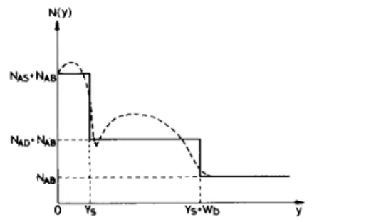
As shown in (2) and (34), several model parameters need to be determined in order to calculate the threshold voltage, the drain current, and the substrate current. Re- ferring to our previous papers [ 6 ] , [7], the channel doping profile with double-boron implantations can be approxi- mated by a double-steps profile shown in Fig. 8, and the parameters in the threshold voltage model can be ex- tracted by comparing the measured threshold voltages un- der different substrate biases with the theoretical results as listed in Table I. Using the linear-region resistance ver- sus ( VgKS - VTo
-
i
curve and its slope and inter- cept measured from the fabricated MOS devices with dif- ferent mask channel lengths, as described in [6], [SI, [9],the effective channel lengths of the fabricated conven- tional and LDD MOS devices and the model parameters listed in Table
I1
can be extracted. Using the extracted parameters listed in Tables I and 11, the drain currents of conventional and LDD MOS devices operated in the lin- ear region can be calculated. In order to fit the drain andHUANG A N D W U : SATURATION MODEL FOR DRAIN A N D SUBSTRATE CURRENTS OF MOSFET'S
: S T
do(um) A o ( m / V ) Conventional 0.230 6 . 7 1 ~ 1 0 - ~ ~ I673 S O ( V / o a ) 3 . 0 0 ~ 1 0 ~substrate currents in the saturation region simultaneously, the model parameters in ionization coefficient ( A o and B o ) and the flowing path depth of the drain current in the PTDA section near the channel side ( d o ) must be opti- mized. In our optimization process, two kinds of errors based on (1) and (34) are defined. One is the error for the drain current, which is expressed as
ERd, =
c
1
I d \ . e x p . f - & / \ . \ , " l . f ( L f ( 3 6 )the other is the error for the substrate current, which is expressed as
where the subscripts of sim, exp, and i represent the sim- ulation results, experimental data, and different bias con- ditions or geometric structures, respectively.
Applying the least squares method to (37), A. and Bo can be determined by solving the following equations:
and
Azi In (Ao)
+
&BO = ( 3 9 )where A l l , A , , , A , , , A*,, B , , , and B Z I are defined in Ap- pendix IV.
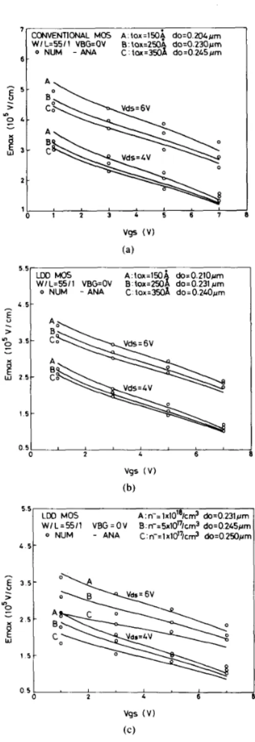
Based on (36) and (37), do can be determined as these two errors are within the assigned values. The flow chart for determining Ao, Bo, and do is shown in Fig. 3, and the extracted values are listed in Table 111. Using the ex- tracted parameters listed in Tables I1 and 111, the drain and substrate currents in the saturation region can be calcu- lated.
IV. COMPARISONS BETWEEN EXPERIMENTAL RESULTS
AND SIMULATIONS
Using the extracted model parameters described in the previous section, Figs. 4 and 5 show comparisons be- tween the experimental data and the developed model for the drain and substrate currents of conventional MOS de- vices, and good agreements are obtained for conventional
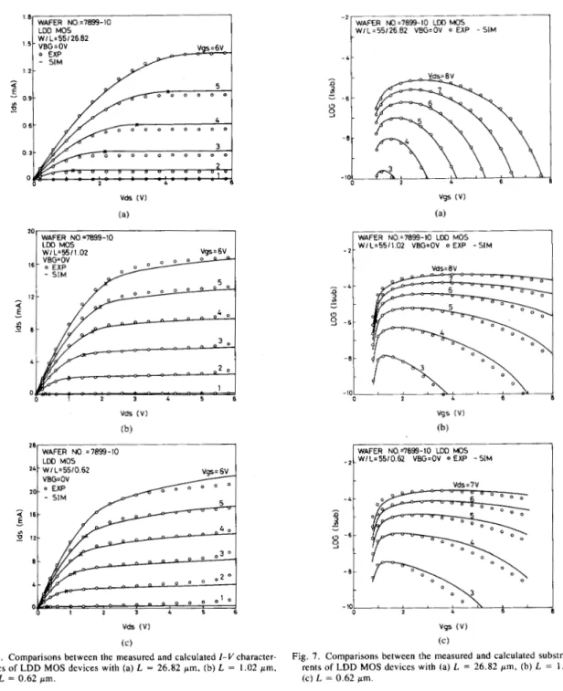
MOS devices with a wide range of channel lengths and bias conditions by using only a set of extracted parame- ters. The asterisks on the I-V curves indicate the calcu- lated saturation voltages. It is easy to see that the calcu- lated drain current is continuous at the transition between the linear and saturation regions. This consequence is mainly due to the fact that the derived A L , is equal to zero at the onset of the saturation condition. Note that the ef- fect of carrier impact ionization has been neglected in the linear region, and the calculated substrate current shown is only limited to the saturation region. However, the in- teresting range of the substrate current is almost included. Similarly, Figs. 6 and 7 show comparisons between the experimental data and the developed model for the drain and substrate currents of LDD MOS devices. It is clearly
t
A N O T H E R V A L U E
Fig. 3. The flow chart for determining d(,, A(,, and B,,
seen that satisfactory agreements are also obtained for LDD MOS devices with a wide range of channel lengths and bias conditions by using only-a set of extracted pa- rameters even though ALz may extend outside the gate region for some bias conditions. It should be noted that the implanted dose in the n- region of the fabricated LDD devices is 3 X 10"/cm2 which is equivalent to the doping concentration of about 10"/cm3; the measured substrate currents do not exhibit the double-hump characteristics.
V. CONCLUSIONS
In this paper, an analytic saturation model has been de- veloped for conventional and LDD MOS devices by using the pseudo-two-dimensional approximation in the channel and drain regions to simultaneously obtain both the chan- nel length modulation factor and the maximum electric field. Using our published models for the I-I/ character- istics in the linear region, the drain currents of conven- tional and LDD MOS devices in the saturation region are analytically derived. The calculated drain current is shown to be continuous at the transition between the linear and saturation regions. Using a simplified substrate current formula and the derived maximum electric field, the sub- strate currents of conventional and LDD MOS devices can be easily calculated. The extraction techniques for the model parameters in the derived I-V model are presented. Furthermore, the accuracy of the developed maximum electric field model for conventional and LDD MOS de- vices is verified by a 2-D numerical analysis. In order to verify the accuracy of the developed saturation model, the calculated drain and substrate currents are compared with the experimental results measured from the fabricated test
1674 IEEk TRANSACTIONS O N tLEC'lRON IIEVICES. V O L . 37. NO. 7. JULY 1990 Vds (V) (a) WAFER No.7899-5 CONVENTIONAL MOS w / L=55/ 1.2 VBG=OV Vds (V) (C)
Fig. 4. Comparisons between the measured and calculated I-V character- istics of conventional MOS devices with (a) L = 26.7 pm, (b) L = 1.2 pm, (c) L = 0.9 pm.
devices with conventional/LDD MOS structures, and a good agreement is obtained for a wide range of channel lengths and bias conditions by using a set of extracted parameters. Therefore, the developed I-I/ model can be used for device design and circuit analysis in a CAD sys- tem.
APPENDIX I
For a MOSFET operated in the saturation region, the drain current will spread out from the pinch-off point to
- 2
WAFER NO ~7859-5 CONVENTIONAL MOS WILz55126.7 VBGzOV 0 U P - SIM
WAFER NO ~ 7 8 5 9 - 5 CONVENTIONAL MO5 W/L=55/1.2 VBG=OV 0 EXP - SIM
-10 -8 - 8
i
- 10 vds=7v 2 L 6 vgs (V) (C)Fig. 5 . Comparisons between the measured and calculated substrate cur- rents of conventional MOS devices with (a) L = 26.7 pm, (b) L = l .2 pm, (c) L = 0.9 pm.
the drain region, and the depletion width below the drain current is a complicated function along the channel direc- tion. For simplicity, it is assumed that
Yo( r )
4l
s
N ( Y ) d Ycan be calculated by averaging the integrations in the GCA
section and in the drain region, and the depletion width under the drain region is constant along the drain direc-
HUANG A N D WU: SATURATION MODEL FOR DRAIN A N D SUBSTRATE CURRENTS OF MOSFET'S
- 2
1675
WAFER N0.-"1899-10 LDD MOS W/L=5510.62 VBGzOV OEXP -SIM WAFER NO ~ 7 8 9 9 - 1 0 LDD MOS W / L= 551 26 82 1 8 1 2 20 16 12 6
-
v) 0 8 4 0 ~ WAFER NO=7899-10 L W MOS W I L=55/1.02 VdS ( V ) (b) 28I
WAFER NO =7899-101
vgs (V) (a) WAFER NO=7899-10 L W MO5 W/L=5511.02 VBG=OV o EXP - 5 I M- 2
-
-I.il
-10 - 8Fig. 6. Comparisons between the measured and calculated I-V character- istics of LDD MOS devices with (a) L = 26.82 pm, (b) L = 1.02 pm,
(c) L = 0 . 6 2 pm.
Fig. 7 . Comparisons between the measured and calculated substrate cur- rents of LDD MOS devices with (a) L = 26.82 pm, (b) L = 1.02 p m .
(c) L = 0 . 6 2 pm.
Yd is the depletion width in the GCA section, which can be obtained from the formula in [7]; W , is the depletion
1676 I E E E TRANSACTIONS ON ELECTRON DEVICES. VOL. 77. NO. 7. J U L Y IWI)
width under the drain region, which can be easily calcu- lated from the one-dimensional Poisson's equation; d; is the spreading depth of the drain current at the pinch-off point, which can be expressed as
where E, is the surface electric field and can be calculated from [7]. It is noted that db is always less than Y</.
The integration of
can be expressed as r do
Note that SA, SB, and
SC
used above can be explicitly calculated by using the step-profile approximation. For a double-channel-implanted profile as shown in Fig. 8, we0 vs Y
Fig. 8. A schematic diagram showing the double-channel-implanted prn- file approximated by a step protile.
by setting E = E,.. In order to simplify the analysis, the
drain current in PTDA section is assumed to be equal to
I d s a t , so the mobile charge density in (7) and (8) can be written as
APPENDIX I11
obtain Using the boundary conditions in (17), we can obtain
SA = (NAs
+
NAB)( Yd-
d ; ) , for Y, I Y,can be rewritten as = N A S ( K -
4 ) +
N A D W ~+
NAB(Y(/ - d b ) ,202E2 = ( 0 ,
+
0 , ) E ,+
( 0 , - B1)F1 - 02Qh (A10)202F2 = (02 - B I ) E l
+
(02+
0I)FI - &Qb. ( A l l ) Multiplying (A10) by ( A l l ) , A L 2 can be omitted, andfor Y,
+
W, I Yd ('44)SB = (NAD
+
NAB)Wd, forRj+
W , I Y,+
W,= ( Y ,
+
W, - R,)NAD+
N A B W ~ , (24) can be obtained.for Rj
+
W , 2 Y,+
W, (A5 ) APPENDIX IVApplying the least squares method to (37), we can ob- tain
= NASY,
+
NADwb+
NABdo, for Y,+
w,
I do. and= 0. (A13)
(Ab) dERsub
dB0
APPENDIX I1
The mobile carriers in PTDA section are assumed to move with the saturation velocity. However, the mobility be overestimated by using V , , = p n E , ( E , = 1//3). In
onset of saturation is equal to V,,/2 which can be ob- tained from
Using (A12) and (A13), the coefficients in (38) and (39) can be easily obtained as
model used in the text is a hyperbolic form, and V , , will order to improve this deficiency, the drift velocity at the
A , , =
C
1 (A14) (A151 A21 = -A12 ('416) ('417) I -1 = ~ 1 Emax,wn,i PI, E -1 Vdnft = ~ A22 =C
~ E 1+ -
E, 1 Eiax,\im.iHUANG A N D W U : SATURATION MODEL FOR DRAIN A N D SUBSTRATE CURRENTS OF MOSFET‘S
~
1677
Isub, exp, i
ACKNOWLEDGMENT
The authors wish to thank the Electronics Research and Service Organization (ERSO), Industrial Technology Re- search Institute (ITRI), Taiwain, Republic of China, for providing the test key, and Dr. M. C. Chen and Dr. H. C. Cheng of the Advanced Semiconductor Device and Technology Research Division, National Chiao-Tung University, for their helpful discussions.
REFERENCES
[I] Y. A. El-Mansy and A. R. Boothroyd, “A simple two-dimensional model for IGFET operation in the saturation region,” IEEE Trans.
Electron Devices, vol. ED-24, no. 3, p. 254, 1977.
[2] P. K. KO, R. S . Muller, and C. Hu, “A unified model for hot-electron currents in MOSFETs,” in IEDM Tech. Dig., p. 600, 1981. [3] T. Y. Chan, P. K. KO, and C. Hu, “Dependence of channel electric
field on device scaling,” IEEE Electron Device Lett., vol. EDL-6, no. 10, p. 551, 1985.
[4] S . Tanaka, S . Saito, S. Atsumi, and K. Yoshikawa, “A self-consist- ence pseudo-two-dimensional model for hot-electron current in MOST’S,” IEEE Trans. Electron Devices, vol. ED-33, no. 6, p. 743, 1986.
[5] K. Mayaram, J. C. Lee, and C. Hu, “A model for the electric field in lightly doped drain structures, ” IEEE Trans. Electron Devices,
vol. ED-34, no. 7, p. 1509, 1987.
[6] G. S. Huang and C. Y. Wu, “An analytic I-Vmodel for lightly doped drain (LDD) MOSFET devices,” IEEE Trans. Electron Devices, vol. ED-34, no. 6, p. 1311, 1987.
[7] C. Y. Wu, G. S . Huang, and H. H. Chen, “An analytic threshold voltage model for short-channel enhancement mode n-channel MOS- FET’s with double boron channel implantation,” Solid-state Elec-
tron., vol. 29, no. 4, p. 387, 1986.
[8] C. Y. Wu, Y. W. Daih, and H. H. Chen, “A structure- and process- oriented model for the I-V characteristics of small geometry n-channel enhancement mode MOSFET with single-channel boron implanta- tion,” Proc. Nut. Sci. Council, Republic of China, p t . A: Phys. Sci.
Eng., vol. 10, no. 4, p. 335, 1986.
[9] C. Y. Wu and Y. W. Daih, “An accurate mobility model for the I-V characteristics of n-channel enhancement-mode MOSFET’s with single-channel boron implantation,” Solid-State Electron., vol. 28, no. 12, p. 1271, 1985.
[lo] T. Y. Chan, P. K. KO, and C. Hu, “A simple method to characterize substrate current in MOSFET’s,” IEEE Trans. Electron Device Lett., vol. EDL-5, no. 12, p. 505, 1984.
[ l l ] I . Hui, F. C. Hsu, and J. Moll, “A new substrate and gate current phenomenon in short-channel LDD and minimum overlaps devices,”
IEEE Electron Devices Lett., vol. EDL-6, no. 3, p. 135, 1985.
M. K. Orlowski, C. Werner, and J. P. Klink, “Model for the electric field in LDD MOSFET’s-Part I: Field peak on the source side,”
IEEE Trans. Electron Devices, vol. 36, no. 2, p. 375, 1989.
H. Katto, K. Okuyama, S . Meguro, R. Nagai, and S. Ikeda, “Hot camer degradation modes and optimization of LDD MOSFET’s,” in
IEDM Tech. Dig., p. 774, 1984.
*
Gwo-Sheng Huang (S’85) was born in Chiayi, Taiwan, Republic of China, on November 4, 1959. He received the B.S. degree from National Cheng-Kung University and the M.S. degree from National Chiao-Tung University, Taiwan, Repub- lic of China, in 1982 and 1984, respectively, both in electrical engineering.
He has been a Ph.D. candidate at the Institute of Electronics, National Chiao-Tung University, and expects to finish his Ph.D. dissertation in the spring of 1990. His research area has been in sub- micrometer MOS device modeling and characterization.
*
Ching-Yuan Wu (S’69-M’72) was born in Tai- wan, Republic of China, on March 18, 1946. He received the B.S. degree from the Department of Electrical Engineenng, National Taiwan Univer- sity, Taiwan, Republic of China, in 1968, and the M.S. and Ph.D. degrees from the State University of New York (SUNY) at Stony Brook, in 1970 and 1972, respectively.
During the 1968-1969 academic year, he served in the Chinese Air Forces as a Second Lieutenant. During the 1972-1973 academic year, he was appointed as a Lecturer at the Department of Electrical Sciences, SUNY, Stony Brook. During the 1973-1975 academic years, he was a Vis- iting Associate Professor at National Chiao-Tung University (NCTU), Tai- wan, Republic of China. In 1976, he became a Full Professor in the De- partment of Electronics and the Institute of Electronics, NCTU. Dunng 1974-1980, he had been the Director of Engineering Laboratories and Semiconductor Research Center, NCTU. He was a principal investigator of the National Electronics Mass Plan-Semiconductor Devices and Inte- grated-Circuit Technologies, during 1976-1979. He had been the Director of the Institute of Electronics, NCTU, during 1978-1984. Since 1984, he has been the Dean, College of Engineering, NCTU. He has also been a Research Consultant at the Electronics Research and Service Organization (ERSO), ITRI, and an Academic Advisory Member of the Ministry of Ed- ucation, Republic of China. His research activities have been in semicon- ductor device physics and modeling, integrated-circuit designs, and tech- nologies. His present research interests focus on small-geometry devices in VLSI, CMOS latch-up, new devices, and technologies. He has pub- lished over 140 papers in the semiconductor field. He received the Aca- demic Research Award in Engineering from the Ministry of Education (MOE), in 1979, and the Outstanding Scholar award from the Chinese Ed- ucational and Curtural Foundation, Republic of China, in 1985; and has received the Outstanding Research Professor fellowship from the MOE and the National Science Council (NSC), Republic of China, during 1982-1991.