國 立 交 通 大 學
電子工程學系 電子研究所
碩 士 論 文
40 奈米製程技術操縱在低操縱電壓及管線結構的
512Kb 8T 靜態隨機存取記憶體
40nm Low V
MINPipeline 512Kb 8T SRAM Design
研 究 生:朱俐瑋
指導教授:莊 景 德 教授
40 奈米製程技術操縱在低操縱電壓及管線結構的
512Kb 8T 靜態隨機存取記憶體
40nm Low V
MINPipeline 512Kb 8T SRAM Design
研 究 生:朱俐瑋 Student:Li-Wei Chu
指導教授:莊景德 教授 Advisor:Prof. Ching-Te Chuang
國 立 交 通 大 學
電 子 工 程 學 系 電 子 研 究 所
碩 士 論 文
A Thesis
Submitted to Department of Electronics Engineering and Institute of Electronics
College of Electrical Engineering and Computer Engineering National Chiao Tung University
In Partial Fulfillment of the Requirements for the Degree of
Master of Science in
Electronics Engineering Sep. 2012
Hsinchu, Taiwan, Republic of China
40 奈米製程技術操縱在低操縱電壓及管線結構的
512Kb 8T 靜態隨機存取記憶體
學生:朱俐瑋 指導教授:莊景德 教授
國立交通大學電子工程學系電子研究所
摘 要
由於現在的3C產品對整個生活週遭影響越來越大,而這些商品一定都需要記憶 體來存放資料。而記憶體的存放或是讀取時間也是會影響整個電子產品的在運作 上之效率。在靜態隨機存取記憶體裡,因為他跟其他的記憶體相比有較快的處理 速度,一般都是放在CPU附近當作快取記憶體,但相較面積之下,確是相對大一 些。所以在先進的SoC晶片設計中,靜態隨機存取記憶體往往都是占整個晶片最 大的面積。由於這個理由,我們必需好好設計他的操作速度及能量消耗。在一般 靜態隨機存取記憶體結構中,主要是以6個電晶體為目前的趨勢。但隨著現在電 子業產品的走向,是希望能在越低的操作電壓中運作,使得整個產品耗電量能越 少越好,6個電晶體的靜態隨機存取記憶體架構會在低電壓中難以正常操作。故 我們設計了一個8個電晶體的靜態隨機存取記憶體能比傳統6個電晶體的靜態隨 機存取記憶體操作在更低的電壓,相對來說,也就比較省電能。為了幫助能在低 壓下寫入/讀取成功,我們在此40奈米512kb的記憶體中加入了提升字元線的機制 以及幫助寫入的電路設計。雖然8個電晶體的靜態隨機存取記憶體原來就比傳統 的靜態隨機存取記憶體操作速度快,但還是能夠比其他的記憶體動作快。我們為 了提升此8個電晶體的靜態隨機存取記憶體之操作速度,我們運用了漣波位元線 讀取架構及管線結構來增進它。40nm Low V
MINPipeline 512Kb 8T SRAM Design
Student: Li-Wei Chu Advisors: Prof. Ching-Te Chuang
Department of Electronics Engineering & Institute of Electronics
National Chiao-Tung University
ABSTRACT
As 3C products now growing impact on the entire lives goods must have the memory to store data. Memory storage or read time also will affect the operational efficiency of the entire electronic product. Relatively faster processing speed compared with other memory in the SRAM, which are generally on the CPU as a cache near, but compared to the area that indeed larger some. So in advanced SoC chip design, SRAM area often is the largest in total chip. For this reason, we must have a good design performance and energy consumption. In general SRAM, the 6T structure is current trend. However, with the trend of the electronics industry, which is hoping to operate in a lower working voltage, power consumption can be as little as possible in the entire product. But the 6T SRAM architecture in low voltage is difficult to operate normally. Therefore, we have designed an 8T SRAM than 6T SRAM operating at lower voltage. Relatively speaking, there is more power savings for products. In order to help write/read mechanism achievement, we use the boosting WL mechanism as well as to help write in 40nm 512 Kb memories circuit design. 8T SRAM operating speed is slower than conventional 6T SRAM, but still faster than other memories. In order to enhance our 8T SRAM speed, we use a ripple bit-line and pipeline structure to enhance it.
誌 謝
本篇論文能夠完成,首先要感謝的是我的指導教授莊景德教授,很幸運地能 夠當他的學生,不僅是個負責、認真,又是個和藹的老師,有困難時也會給我很 多的建議,也許我是女孩子吧,老師總是會比較關照及希望不要太給我太大的壓 力(但該有的壓力還是有的),我想應該是上輩子有做好事還有這輩子有積陰德所 換來的吧! 再來就是要感謝在這個論文中也給我很多幫助的在職博班學長連南鈞學長。由 於學長在業界打滾許久,所以研究上有一些問題的時候總是能馬上抓出重點,及 電路上的改良設計也幫忙不少,讓我省了不少力,還有謝謝智原公司的學長們(明 賢、Jason、Jerry、Angelo、Paul)大力贊助才能成就此篇論文結果如此的完美。 另外還有實驗室的已經畢業的學長們能分享在電路設計上的技巧及設計和能陪 我玩桌遊的學弟妹們,讓我有個充實學習又不失快樂的實驗室環境。 最後感謝我的父母,沒有他們也就沒有現在在交大讀書的我。還有感覺像朋友 的弟弟,雖然讀的是不同的科系(資工系),但有時也會給點看法並給我一些幫助。 另外,住在交大附近的表姊、表姊夫及他們的好友們讓我在新竹有困難時能給我 一些援助,讓我感覺在新竹一點也不孤單。I
Contents
Chapter 1 Introduction ... 1
1.1 Background ... 1 1.2 Motivation ... 1 1.3 Thesis Organization ... 2Chapter 2 Overview of Low-voltage SRAM Design in Recent Years . 4
2.1 Introduction ... 4 2.2 Memory Family ... 4 2.2.1 Flash ... 4 2.2.2 DRAM ... 6 2.2.3 FinFET SRAM ... 8 2.3 SRAM ... 11 2.3.1 6T SRAM ... 11 2.3.2 Conventional 8T SRAM ... 142.4 SRAM Static Noise Margin (SNM) ... 15
2.4.1 Hold Static Noise Margin (HSNM) ... 16
2.4.2 Read Static Noise Margin (RSNM)... 17
2.4.3 Write Static Noise Margin (WSNM)... 19
2.5 SRAM Write Margin (WM) ... 20
2.6 SRAM Array Structure ... 21
2.7 Variation Issue ... 23
2.7.1 Global and Local Variation ... 23
2.7.2 SRAM Cell Variation ... 26
2.8 Modern SRAM Design Methodology ... 29
2.8.1 Dual Supply Voltage ... 29
2.8.2 Negative Bit-Line ... 32
II
2.9 Power Consumption ... 38
2.9.1 Dynamic Power Dissipation ... 38
2.9.2 Short-Circuit Power Dissipation ... 39
2.9.3 Static Power Dissipation ... 40
Chapter 3 40m 512Kb Pipeline Low VDD 8T SRAM ... 44
3.1 Introduction ... 44
3.2 8T SRAM Operation ... 45
3.2.1 Conventional Single-Ended 8T SRAM ... 45
3.2.2 Disturb-free DAWA Single-Ended 8T SRAM ... 46
3.3 Data-Aware Write-Assist (DAWA) and Interleaving ... 49
3.4 Pipeline Structure and Clock Distribution ... 51
3.5 Word-Line Booster ... 54
3.5.1 Word-Line Booster Circuit ... 54
3.5.2 Booster Capacitance Design ... 56
3.5.3 Simulation Result ... 57
3.6 Voltage Detector ... 58
3.6.1 Voltage Detector Design ... 58
3.6.2 Simulation Result ... 60
3.7 Data-Aware Write-Assist Tracking Circuit ... 61
3.7.1 DAWA Tracking Circuit Design ... 61
3.7.2 Simulation Result ... 63
3.8 Ripple Bit-Lin (BL) and Multiplexer ... 64
3.8.1 Ripple BL and Multiplexer Designs ... 64
3.8.2 Simulation Result ... 67
3.9 The Keeper Design of LBL ... 68
3.9.1 The Keeper Design ... 68
III
3.10 Data-In Data-Out (DIDO) Design ... 75
3.10.1 GBL Latch ... 75
3.10.2 Write Through Circuit ... 77
Chapter 4 The Chip Structure Result ... 79
4.1 Chip Sepc. ... 79
4.2 Chip Per-Simulation vs. Post-Simulation ... 81
4.3 Test Flow ... 83 4.4 Testing Result ... 86
Chapter 5 Conclusion ... 90
5.1 Conclusion. ... 90Reference ... 91
Chapter 1 ... 91 Chapter 2 ... 91 Chapter 3 ... 94Vita ... 98
IV
List of Figures
Fig. 1.1 (a) Conventional 8T SRAM cell (b) single-ended 8T SRAM cell ... 2
Fig. 2.1 Schematic cross section of the Flash cell [2.1] ... 5
Fig. 2.2 NOR Flash writing mechanism [2.1] ... 5
Fig. 2.3 Floating-gate MOSFET reading operation [2.1] ... 6
Fig. 2.4 DRAM structure ... 7
Fig. 2.5 Multi-fin FinFET [2.3] ... 8
Fig. 2.6 TG-FinFET 6TSRAM cells schematic [2.4] ... 9
Fig. 2.7 TG-FinFET 6T SRAM cells layout [2.4] ... 10
Fig. 2.8 IG-FinFET 6T SRAM cells schematic [2.4] ... 10
Fig. 2.9 IG-FinFET 6T SRAM cells layout [2.4] . ... 11
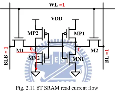
Fig. 2.10 6T SRAM cell structure . ... 11
Fig. 2.11 6T SRAM read current flow ... 12
Fig. 2.12 6T SRAM writing current flow . ... 13
Fig. 2.13 6T SRAM transistor ratios . ... 13
Fig. 2.14 Conventional 8T SRAM ... 14
Fig. 2.15 Conventional 8T SRAM layout [2.5] . ... 15
Fig. 2.16 Voltage transfer curve of inverter [2.6] ... 16
Fig. 2.17 HSNM detected circuit ... 16
Fig. 2.18 The butterfly curve in hold mode ... 17
Fig. 2.19 RSNM detected circuit ... 18
Fig. 2.20 The butterfly curve in read mode (6T) ... 18
Fig. 2.21 The 8T butterfly curve in read mode ... 19
Fig. 2.22 WSNM detected circuit ... 19
Fig. 2.23 The write-1 VTC ... 20
Fig. 2.24 Diagram of new write margin [2.8] ... 20
V
Fig. 2.26 SRAM critical path [2.9] ... 22
Fig. 2.27 Global variation and Local variation of VT [2.10] ... 23
Fig. 2.28 (a) Number of dopant atoms in the channel as function of effective channel length (b) “sigma” of VT variation of function of technology node ... 24
Fig. 2.29 Plot of randomly generated dopant positions in a 25nm MOSFET, viewed from the side. [2.12] ... 25
Fig. 2.30 Plot of threshold voltage uncertainty (1σ) versus the vertical depth parameter, d, of the source /drain doping for 25nm n-channel MOSFETs, comparing discrete donor effects to discrete acceptor effects. [2.12] ... 26
Fig. 2.31 Scaling and cell stability margin of 6T [2.13] ... 27
Fig. 2.32 6T RSNM with VT variation [2.11] ... 28
Fig. 2.33 The effect of local variation in write-mode with worse case ... 29
Fig. 2.34 The effect of local variation in read-mode with worse case ... 29
Fig. 2.35 Single-Vcc and Dual-Vcc processors [2.14] ... 30
Fig. 2.36 (a) Cell stability in the Vmin (b) Vnim in different bit desnsity [2.14] .. 30
Fig. 2.37 The cross-point 8T SRAM schematic, layout, read/write negative-biased circuit, and waveform [2.15] ... 31
Fig. 2.38 Constant-negative-level write buffer. [2.16] ... 32
Fig. 2.39 Simulated negative bit-line level. [2.16] ... 33
Fig. 2.40 Write driver with boost control [2.17] ... 34
Fig. 2.41 Write cycle simulation waveforms and results l [2.17] ... 34
Fig. 2.42 SNM improvement by lowering WL voltage in 6T SRAM in case of (a) with and (b) without local VT variations. [2.18] ... 35
Fig. 2.43 Improving read stability depending on process and temperature variations. [2.18-19] ... 36
Fig. 2.44 Write assist circuit (WAC) improving write stability [2.18-19] ... 37
Fig. 2.45 (a) Simulated waveform of the ary-VDM and dmy-VDM in the write status. (b) Comparison of the write ability by DC simulation result of the write-trip-point. [2.19] ... 37
VI
Fig. 2.46 The inverter schematic [2.20] ... 38
Fig. 2.47 Current behavior of an inverter without load. [2.21] ... 39
Fig. 2.48 Leakage components in a scaled transistor [2.22] ... 40
Fig. 2.49 Injection of hot electrons from substrate to oxide [2.23] ... 41
Fig. 2.50 As n+ region is depleted or inverted with high negative gate bias, condition of the depletion region near the drain-gate overlap region of an MOS transistor [2.23] ... 42
Fig. 2.51 Variation of minority carrier concentration in the channel of a MOSFET biased in the weak inversion. [2.23] ... 42
Fig. 3.1 (a) A conventional single-ended 8T SRAM cell.[3.11] (b) A disturb-free DAWA single-ended 8T SRAM cell. [3.12] ... 45
Fig. 3.2 (a) The operation for stand-by mode. (b) The read-mode operation. (c) The operation for wirte-1 mode. (d) The operation for write-0 mode. ... 47
Fig. 3.3 Cell layout for disturb-free DAWA single-ended 8T SRAM. ... 48
Fig. 3.4 Write-1 mode and write-0 mode with half-select ... 50
Fig. 3.5 Interleaving array structure ... 51
Fig. 3.6 The CLK signal use H-tree way. The black line represents the farthest path of CLK and the black cycle stand for the farthest cell. And the red line represents the nearest path of CLK and the red cycle stand for the nearest cell. ... 52
Fig. 3.7 The master-slave latches. The master latch part enclosed by the red wireframe; then slave latch part enclosed by the green wireframe. The master latch capture data in the positive clock, we called the latch of L1. Also, the slave latch to do is launching the data, we called the latch of L2. ... 53
Fig. 3.8 The pipeline SRAM operation in whole chip ... 54
Fig. 3.9 (a) Write margin of writing 0 with boosting. (b) Write margin of writing 1 with boosting. ... 55
Fig. 3.10 The wordline booster which BST_EN come from voltage detector. If we want to boost WL, then the BST_EN signal goes high, vice versa. ... 55
VII
Fig. 3.12 Boosting ∆v steps. ... 57
Fig. 3.13 The simulation of WL, farthest cell array write/read, and data-out (DO) ... 58
Fig. 3.14 (a) The delay chain by the CSB controlled. (b) The section by an external voltage to decide whether or not as boosting WL. (c) Three different corner (SS, TT, FF) be controlled by OSD<0>~<2>. voltage at VDD is 0.9 ... 59
Fig. 3.15 The simulation waveform of voltage detector. ... 60
Fig. 3.16 DAWA tracking circuit. ... 61
Fig. 3.17 1-bit dummy cell and tied 0/1 schematic. ... 62
Fig. 3.18 DAWA tracking circuit waveform @ TT, 25℃, VDD=1.1V, OSD<0>: on. ... 63
Fig. 3.19 The ripple path structure and the LEV_TOP and LEV_DN read part circuit. ... 64
Fig. 3.20 The ripple multiplexer circuit ... 65
Fig. 3.21 The waveform for the ripple multiplexer ... 67
Fig. 3.22 (a) The keeper of ripple multiplexer, (b) the keeper of LEV_TOP, and (c) the keeper of LEV_DN in red part ... 69
Fig. 3.23 LCR keeper dynamic gate topology [3.22] ... 69
Fig. 3.24 The waveform by replica keeper @ ff, 125℃, VDD=1.1V. ... 70
Fig. 3.25 Read local bit-line with contention free shared (CFS) keeper and global keeper delay element. [3.23] ... 71
Fig. 3.26 The waveform for GBL by CFS keeper @ ff, 125℃, VDD=1.1V. ... 72
Fig. 3.27 The local bit-line keeper design in detail ... 72
Fig. 3.28 The local bit-line keeper design is chose from the LBL_KP<0>. ... 73
Fig. 3.29 The local bit-line keeper design is chose from the LBL_KP<1>. ... 74
Fig. 3.30 The waveform for local bit-line keeper design @SS, 125℃, VDD=0.99V ... 75
Fig. 3.31 The GBL latch circuit ... 76
VIII
Fig. 3.33 Writer through design ... 77
Fig. 3.34 Writer through design waveform ... 78
Fig. 4.1 The simple diagram of 512Kb 8T SRAM ... 79
Fig. 4.2 Cycle time diagram for read/write ... 80
Fig. 4.3 Signal line distribution in chip ... 81
Fig. 4.4 Po-sim vs. pre-sim @ TT, 25℃, VDD=1.1V ... 82
Fig. 4.5 Po-sim vs. pre-sim @ FF, -40℃, VDD=1.21V ... 82
Fig. 4.6 Po-sim vs. pre-sim @ SS, 125℃, VDD=0.99V ... 83
Fig. 4.7 The design places on half chip. ... 83
Fig. 4.8 The chip testing flow. ... 85
Fig. 4.9 The layout of chip. ... 86
Fig. 4.10 The function check for chip. ... 86
Fig. 4.11 The function check for chip. ... 86
List of Table
Table 3.1 Disturb-free new 8T SRAM operation ... 48Table 3.2 GBL_KP voltage on different corner ... 70
Table 4.1 Pin descriptions for the chip . ... 80
Table 4.2 Three options for the chip. . ... 87
Table 4.3 The pass rate for TT, 25℃ . ... 87
Table 4.4 The pass rate for FF, 25℃ . ... 87
1
Chapter 1
Introduction
1.1 Background
In the IC’s world, we are following the Moore’s Law today. In another word, the density of the chip will become double each 18 months. So we can design more complex circuit and improve performance at the same area in the past nano-technology. For this reason, the most of market’s 3C products are becoming smaller, light and portable. Cause of the size of the transistor trend is getting smaller; we wish the power consumption reduce, too. Beside, the leakage current and the process pass into more important and critical. These problems should research and study in today IC products.
The memory area will occupy around 90% of the system on SOC base on the International Technology Roadmap for Semiconductors (ITRS). The prediction tells us the Static Random Access Memory (SRAM) will affect the total power dissipation and area seriously. The modern smart phone and note book has begun to keep watch for power, because they should use the battery to work. And they internal circuits both have the SRAM, so we will reduce the SRAM power is the major and important work.
1.2 Motivation
Governments around the world advocate use power effective and saving energy. Moreover, the IC companies also want to reduce the support external power for their produces. That show us the power is an important role, not only hope use it available but also how to decrease the power in recent years. As a result of the subject, I choose the SRAM in order to cut down the total power as best as possible.
2
For reading a lot papers and listening memory classes, I realize the 8T SRAM is the best choice. In spite of 8T SRAM’s speed is lower than conventions 6T SRAM, but it can work at lower power than 6T SRAM. Well-known manufacturers like IBM publish paper that their SRAM also use 8T SRAM due to diminish power dissipation. Besides, 8T SRAM has a better ability of read-disturb than 6T SRAM which the read disturb is free that allows a robust operation in lower voltage supply. And I show the conventional 6T cell and the single-ended 8T SRAM cell below the article (fig. 1.1) [1.1].
1.3 Thesis Organization
The thesis will introduce you the overview Low-Voltage SRAM design in chapter 2. I will discuss and analyze the low-voltage SRAM development. Afterwards, how to produce the power consumption and have to take notice of the current leakage from the transistor that also writes in chapter 2.
In chapter 3, I will tell you my 8T SRAM design structure in detail. I want to do the design better and use some circuit to improve the performance in the 512Kb memory chip. The 8T SRAM chip use the pipeline structure that wishes the performance can get better and working faster. Besides, we choose the H-tree clock distribution to
Q B Q W B L W B L B R B L R W L W W L Q B Q W B L W B L B R B L R W L W W L (a) (b)
3
transmit the external clock that is able to make the pipeline working preferable. Then, the 8T SRAM made Data-Aware Write-Assist (DAWA) to enhance its write ability and reduce power. Then, we use a new scheme of voltage controller that control whether boosting world-line (WL) or not to write/read ability better. Doing DAWA operation, we can’t always turn on the DAWA for long time that the cell data is flipped probably. For this reason, we design the DAWA tracking circuit to control the DAWA switch.
Finally, chapter 4 is displaying the test flow how to test the design and showing the chip measure results. We will discuss the data by real measurement and analyze the design where should modify that let the chip performance better. Chapter 5 is making a conclusion of reference in the thesis.
4
Chapter 2
Overview of Low-Voltage SRAM Design in
Recent Years
2.1 Introduction
The chapter first would introduce the family of memory development and discuss their identity. To realize read-disturb, read static noise margin (RSNM), write static noise margin (WSNM) definitions, and so on. We just choose major memory to realize how they operation in present IC industry.
Next, I will tell you the conventional 6T SRAM, the conventional single-ended 8T SRAM, and the new 8T disturb-free single-ended 8T SRAM basic operation. Even though two single-ended 8T structures are different, but the RSNM and WSNM is the same. Besides, I show the simulations of the 6T/8T SRAM RSNM and WSNM. Since the thesis is talking about power, we discuss the power consumption where produce in the transistor in this chapter ultimately.
2.2 Memory Family
2.2.1 Flash
Flash has developed for 20 years since in 1986 product. The main structure are NOR and NAND flash memories. Its belong Non-Volatile Memory (NVM) and play an important role on disk cashes. It also viable subsystem on PC computing and uses other applications as 3G/UMNT mobile phones. The NOR composition main make use of cellular phones or embedded application and the NAND composition is for memory cards. The NOR flash for code and storage application and the NAND flash only for data storage. [2.1][2.2]
5
We simply explain the flash operation. We see the Fig. 2.1, this is a Flash cell which has two gates surrounding by dielectrics. The couple capacitor is produce between control gate (CG) and floating gate (FG). In normal state (or positively charged), the data is logic “1”. And the negatively charged state stand for the data value is logic “0” as electrics store in the FG.
For writing operation, a NOR Flash is programming by channel hot electron (CHE) injection in the floating gate (FG) at the drain side; it is eared by the flower-nordheim (FN) electron tunneling oxide from the FG to the silicon surface. (Fig. 2.2) [2.1].
Fig. 2.1 Schematic cross section of the Flash cell. [2.1]
6
For reading operation, we can measure the FG MOS transistor voltage to decide the cell data whether is logic “1” or “0”. We see the Fig.2.3 [2.1] that realize the Flash cell store logic “1” that transconductance is the same with logic “0” in current-voltage characteristic curve. Only difference is the threshold voltage shift ∆VT that is proportional to store the electron charge Q in fixed gate bias. While the current is very high we measure that means the stored data is logic “1” in fixed bias voltage. In other case, as we measure the current is 0 that represent the Flash cell storage logic “0”. [2.1]
2.2.2 DRAM
Dynamic Random Access Memory (DRAM) is very important memory for PC that main application is used to most of memory for disk in this day. DARM is the Volatile Memory (VM). If you do not support the fixed voltage for it, the DRAM cell storage data can’t remain original data in last time. The DRAM structure is combined into one transistor and one capacitor as Fig. 2.4. Due to the simple composition (1T+1C) that density is very well. With SRAM comparison, the cost is cheaper than SRAM, but accesses data slower and consumes more power.
7
Next, the DRAM cell is introduced into its operation of reading and writing. In write mode, turns on the access transistor is controlled over word-line at first. If we want to transmit the logic “0” data in the DRAM cell, first step the bit-line (Fig. 2.4) discharge to GND. Then second step, original charges in the storage capacitor are produced the discharged path passing through the access transistor to bit-line. Else if we wish to write logic “1” into the DRAM cell, we assume the storage capacitor has no charge into in beginning. The bit-line charges to the support voltage (VDD) and turns on the access transistor naturally. Then it comes into a charge path from bit-line through the access transistor and finishes the working.
In read mode, of course the cell must turn on the access transistor. The bit-line voltage always is VDD that fixed supporting voltage in stand-by mode. When in read mode, the bit-line voltage changes from VDD to 1/2VDD. Besides, the cell storage logic “1” let the bit-line voltage larger than 1/2VDD. On the contrary, the cell stores logic “0” make the bit-line voltage less than 1/2VDD. This bit-line voltage wills read the result by sense amplifier with 1/2VDD as a diving line.
But cause of the DRAM structure has a capacitor that discharges to ground for period of time. This problem makes the write “1” data in cell for long time, the capacitor voltage change floating “1” to floating “0” and finally read the cell data
8
result is wrong. To solve the problem, there is a mechanism for each fixed time will be recharged once.
2.2.3 FinFET SRAM
According to Moore’s law, today the process gets smaller and smaller but cause to the physical properties discover we will meet the bottleneck below 10nm process. Therefore, some people use the same process however the system place the way of 3D that can improve the performance. Another way is changing the MOS structure, and afresh is issued with properties, and then does modify and modeling. The structure is FinFET that is a trending in the future!
Now we begin to introduce the FinFET composition. There are three FinFETs in Fig. 2.5 [2.3]. This composition unlike planar single- and double-gate devices in plane, the channel width is placed perpendicular to the semiconductor plane. It is not only increase the drive current due to raise per unit planar area by fin-height but also reduces the delay time cause to the equation: Cload/Idrive. [2.3]
9
In the Fig. 2.5, the silicon fin of thickness tsi is located on an SOI wafer. The tsi is
the body-thickness of the resulting double-gate structure where both gates are tied together. Current flow is parallel to the wafer plane while channel width is perpendicular to the plane. The effective channel width is equal to 2h because the height of SOI thickness also is h. Higher widths are achieved by drawing multiple fins in parallel and wrapping the gate around them. The effective channel width for a multi-fin FinFET on a given planar area of silicon is determined by h and fin-pitch p. The minimum h required to achieve equivalent planar are efficiency is thus p/2. In other words, increasing h beyond p/2 increases area efficiency. The upper bound on h is set by the maximum fin aspect ratio (amax=Hmax/ tsi) allowed by the process. [2.3]
The design considerations for the reliable operation of the 6T FinFET SRAM circuits are provided in this section. The standard tied-gate (TG) FinFET SRAM cell is shown at Fig. 2.6 that all six transistors are sized minimum in 32nm process and Fig. 2.7 is that layout. [2.4]
10
The idle mode leakage power consumption is reduced with the Independent-Gate (IG) FinFET 6T SRAM that can enhance the data stability and the integration density as compare to the TG-FinFET SRAM circuits. The schematic is in the Fig. 2.8 and the layout is shown at Fig. 2.9 that the six transistors also use the minimum size.
Fig. 2.7 TG-FinFET 6T SRAM cells layout [2.4]
11
2.3 SRAM
2.3.1 6T SRAM
The 6T SRAM is the most companies using to produce SRAM memory in recent years. The construction is shown in Fig. 2.10. It is composed of two back-to-back inverters and adds one NMOS in inverter input side respectively that accomplishes the 6T SRAM structure. We usually say MP1 and MP2 are pull-up gates; MN1 and MN2 are called pull-down gates; M1 and M2 are called pass-gates in the field. In standby, the 6T SRAM setting is bit-line (BL) and bit-line-bar (BLB) is charging to VDD, but the word-line (WL) is not turning on.
QB Q WL B L B B L MP1 MP2 MN1 MN2 M1 M2 VDD
Fig. 2.9 IG-FinFET 6T SRAM cells layout [2.4]
12
First, we start to introduce the read operation in 6T SRAM. Above the description, the standby mode, the BL and BLB will pre-charge to VDD at beginning. As reading the cell, the selected cell WL is going high (logic “1”) that turns on the M1 and M2. Then, the BL and BLB voltage starts to float. If we assume the Q data is logic “1” and QB is logic “0”, cause to switch on M1 the BLB voltage is going to low gradually until the voltage to GND. The cell right side BL voltage is floating high according to the Q is logic “1”. We can see the Fig. 2.11 to realize the current flows in the 6T cell.
0 1 WL =1 B L B = 1 B L = 1 MP1 MP2 MN1 MN2 M1 M2 VDD
Second, we explain the 6T SRAM write operation. Consider the Q point wish to write logic “0”, so the Q point initial value is logic “1”. Turning on the WL and BL discharge to GND but BLB still keep on VDD. Q is going to write “1” operation and the other side, QB is going to do writing “0” working. In write mode, the BL and BLB are two opposite signals. To see Fig. 2.12 that displays the write operation and current flows. The red numbers are initial values in the figure and the data will be written to the 6T cell in period.
13 0 1 WL =1 B L B = 1 B L = 0 MP1 MP2 MN1 MN2 M1 M2 VDD
After understanding the read/write operation in 6T SRAM, we always want to read and write data easily but these two running conflict each other. If we consider read ability well, the pull-down NMOS must be stronger than the pass-gate NMOS. Else if we wish write ability good, the pass-gate NMOS have to stronger than pull-up PMOS. Unfortunately, we also thick about the stability in standby mode and the pull-up PMOS do not be weaker overly than pull-down NMOS. In Fig. 2.13, there are three ratios β 1, β 2, andβ 3 in blue background that are represented the proportion of standby, read, and write ability. In simple terms,β 1 value cannot much smaller; β 2 value is more smaller more better; β 3 values is more larger more better.
Fig. 2.12 6T SRAM writing current flow
14
2.3.2 Conventional 8T SRAM
Although 6T SRAM performance is very well and simplify the SRAM, but the trend for all 3C products with the external voltage requirements are low. The 6T SRAM external power cannot too low that the reason will explain in below selection. For working in low VDD, we try to design another SRAM cell and the 8T SRAM is produced directly. In Fig. 2.14 is shown the conventional 8T SRAM. [2.5]
QB Q W B L W B L B R B L RWL WWL VDD
This 8T cell (Fig. 2.14) adds two-transistor read stack in the conventional 6T cell. The below transistor gate of the stacking-transistor is connected to the node of Q. While write operation, we just turn on the WWL directly and RWL not turn on. Then the working way is the same by the conventional 6T SRAM cell. Afterwards, the read operation is turning on RWL and turning off WWL that the current only through two stack transistors if the Q value is logic “1”, then RBL is pulled down to logic “0”. If Q is logic “0” that RBL voltage is a floating “1”. In addition, the two cross-coupled inverters of 8T SRAM condition is alike standby state so that don’t have read-disturb problem.
The Fig. 2.15 [2.5] is the conventional single-ended 8T SRAM layout. The compact layout is the 6T cells at the left side that just take on the RWL and RBL at the right side, and then the layout is accomplished. The WWL is 6T cells’ WL. Similarly, the WBL and WBLB are 6T cells’ BL and BLB separately.
15 GND RBL RWL WWL WWL GND GND VDD VDD WBL WBLB N-well Active Gate
However, the thesis 8T SRAM cell schematic is not the above description. We use the different design way and have the same benefits, for example: Read Static Noise Margin (RSNM) is better than 6T SRAM and can work in low VDD. The 8T SRAM we use will introduce in chapter 3.
2.4 SRAM Static Noise Margin (SNM)
Static Noise Margin(SNM) means that the maximum DC noise voltage. In simple words to say that is a bit-cell can be tolerated by the moaximum noise value. If exceed the value, then the storage in the cell will be filed and be incorroected. Measure the SNM is getting form Voltage Transfer Curve (VTC) that usually is called as “butterfly curve” and SRAM cell must have two inverters that place back-to-back. We show Fig. 2.16 that is the VTC of inverter. Besides, we use the example for 6T cell explain SNM for below article.
16
2.4.1 Hold Static Noise Margin (HSNM)
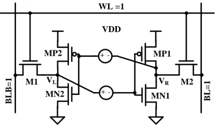
HSNM is means when the SRAM cell in the stand-by mode. The WL signal is logic “0” and do not turn on the cell pass-gate. Next, BL and BL signals are pre-charged logic “1”. Cause of SNM have to use DC voltage to measure, we use the way [2.7] to test the value that shown in Fig. 2.17.
WL =0 B L B = 1 B L = 1 MP1 MP2 MN1 MN2 M1 M2 VDD + + - VR VL
Fig. 2.16 Voltage transfer curve of inverter [2.6]
17
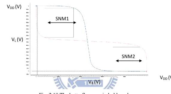
The method of measuring HSNM is connected to two DC noise source with 6T cell in Fig. 2.17. We sweep the DC noise source form high voltage (ex: 1V) to low voltage (ex: 0V), then observing the result of VR and VL voltage. These results individually use the VDD and VR/VL to do two axes that accomplish the voltage transfer curves. VTCs overlapping outcome that the shape like a butterfly, so the mapping also say “butterfly curve” as shown in Fig. 2.18. There are two SNM in the figure, we choose the smaller SNM as the cell SNM.
2.4.2 Read Static Noise Margin (RSNM)
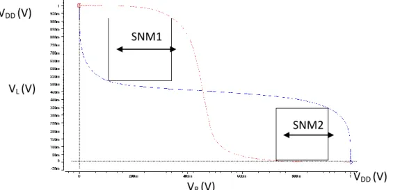
The method is the same as the above description that difference is initial condition. We turn on the WL in read mode and per-charge BL and BLB to VDD are changeless in 6T cell that show in Fig. 2.19. Besides, the butterfly curve is shown in Fig. 2.20. Expressly, the RSNM is worse than HSNM in 6T cell. The reason is that WL turns on the M1 and M2, so produced the current path pass through the pull-down NMOS: MN1 and MN2. Pull-down NMOSs have an equivalent resistor due to the VR/VL voltage cannot low to GND. This voltage difference from the minimum voltage to GND we are called read-disturb.
Fig. 2.18 The butterfly curve in hold mode VR (V) VL (V) VDD (V) VDD (V) SNM1 SNM2
18 WL =1 B L B = 1 B L = 1 MP1 MP2 MN1 MN2 M1 M2 VDD + + - VR VL
In read mode, the 6T cell have the read-disturb problem that the RSHM is worse but the 8T cell will solve the read-disturb problem due to the initial condition is the same in hold mode. The 8T cell in read mode just turns on the RWL and the inside WWL don’t turn on at Fig. 2.14. The 8T RSNM is shown in Fig. 2.21 and the thesis 8T cell also have the same conclusion.
Fig. 2.19 RSNM detected circuit
Fig. 2.20 The butterfly curve in read mode (6T) VR (V) VL (V) VDD (V) VDD (V) SNM1 SNM2 Read-disturb Read-disturb
19
2.4.3 Write Static Noise Margin (WSNM)
In write mode, we assume VR voltage is logic “0”, then VL is logic “1”. Let the WL voltage go high and switch on M1, M2. BL is logic “1” according to VR voltage, for the same reason that LBL is setting logic “0”. The writing operation is ready and use again DC source to input two inverters gate detecting VR/VL variation as shown in Fig. 2.22. As a result of the right-side inverter setting is the same with RSNM, so the one of Voltage Transfer Curve (VTC) is equal in Fig. 2.23.
WL =1 B L B = 0 B L = 1 MP1 MP2 MN1 MN2 M1 M2 VDD + + - VR =0 VL =1 VR (V) VL (V) VDD (V) VDD (V) SNM1 SNM2
Fig. 2.18 The 8T cell butterfly curve in read mode Fig. 2.21 The 8T butterfly curve in read mode
20
2.5 SRAM Write Margin (WM)
Write ability to use other methods this way is to Write Margin (WM). How to survey the value in a cell? We read on. First, we let the BLs to high level (VDD), and sweep down BL form VDD to GND. When the cell storage value is flipped all at once, now the BL voltage is defined as WM. Or change another way to say, we test the BL voltage start from GND to rise gradually as we detect the cell write fail that the voltage is WM. We see the Fig. 2.24 [2.8] to realize the definition.
VR (V) VDD (V)
Fig. 2.23 The write-1 VTC
21
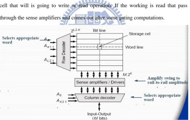
2.6 SRAM Array Structure
Cause of the memory in 3D products is very important that has to save or read many data in the period time, so the designed memory system need to a lot of areas for memory cells. Nevertheless, there is the way to design the memory array structure already and follows it can make well easily. The memory array basic structure is in Fig. 2.25. We always put many memory cells together that is called SRAM array if the memory is by SRAM. The SRAM array left side places the row decoder that working is decoded one signal for address to select a cell word line. Then, the SRAM array below puts a column decoder that running one signal by address to choose a cell bit line. To select one word line and one bit line their across a cell is called storage cell that will is going to write or read operation. If the working is read that pass through the sense amplifiers and comes out after some gating computations.
To design a memory system we have many tests to test. Usually one circuit has one critical path to use tracing a lot of problems. Of course, SRAM organization also has a critical path as in Fig. 2.26. Most of critical paths are the longest of total system by designer. The reason is that the longer path will go through more gates in general. The
22
critical path starts from address and then sequence passes through address register, row decoder, column mux., sense amplifiers, comparator, and finally input/output register in Fig. 2.26. Most of delay is though the SRAM column, column mux., and sense amplifier. If want to reduce the delay time for this case, we should consider to discuss and solve how to cut down the gate delay that the path can be shorter than before.
23
2.7 Variation Issue
2.7.1 Global and Local Variation
As we designed chip is manufactured from factories, anyway there must have some deviations in the real chip. For CMOS process, variations are able to be reflected on the threshold voltage (VT) directly. Because of VT is different from original we are designed, the current drive ability of transistor would be deviated and leakage probably become larger than initial device. The result is even serious enough to outcome failed or produce more power to run the chip. According to the advanced process is smaller in recently, the chip to make for lithography that must have diffraction be produced and comes to more critical.
In a deeper sight to face squarely the formation of variation, we are able to distribute the variation into Global and Local. Global variation has another saying that is called “inter-die variation”. The variation is expressed from die between die each other. And then the Local variation is also called “intra-die variation”. The definition is that the variations of transistors in one die. The two variations are shown in Fig. 2.27 [2. 10].
24
The figure of Fig.2.27 that δ VT can be equal to like this:
δ VT = ∆VT_GLOBAL - ∆VT_LOCAL [2.11]
Besides, Global variation is the variation of environment like that temperature, lithography, machine settings, doping concentration, itself silicon film thickness and so on. We just only pick one selection of the variation to discuss that is doping concentration. At first, we generally realize the information for discrete dopant effect. For the 50nm Leff (90/60nm node) that approximately has 200 dopant atoms in channel; for 12nm Leff (32/28nm node) that approximately has 2.6 dopant atoms in channel; for 8nm Leff (22/20nm node) that approximately has 1.7 dopant atoms in channel. This information tells us that if the process size is smaller, then the variation becomes larger and worse. We can look the Fig. 2.28 to understand that. In the 30nm process, the sigma (σ) of VT variation is raise by a factor of 4.
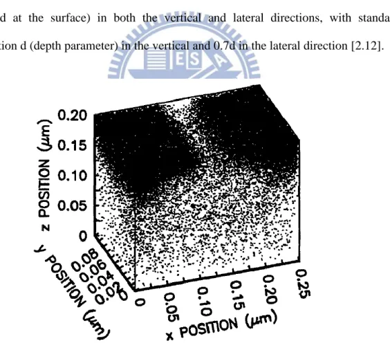
Fig. 2.29 shows an example of dopants positioned using this algorithm for a 25nm nMOSFET design. Using the technique, the threshold voltage fluctuations of many different MOSFET designs have been evaluated. The 0.225x0.2x0.1um simulated
(a) (b)
Fig. 2.28 (a) Number of dopant atoms in the channel as function of effective channel length (b) “sigma” of VT variation of function of technology node
25
volume contained 224550104 Si atom positions, of which 62280 were converted to donors and 12703 were converted to acceptors. Darker dots are donors, lighter dots are acceptors. [2.12]
In addition to demonstrating the advantages of retrograde doping, we have also analyzed the separate effects of donor and acceptor descretiaztion in an aggressive 25nm channel length MOSFET, as shown in Fig. 2.30, which also illustrate that shallower source/drain doping yields smaller fluctuations. Results for a still smaller device design will also be shown, in addition to a study of the dependence of the VT fluctuations on the device width and the nature of the boundary condition in the width direction. Besides, the source/drain doping profile is modeled as a Gaussian (1020 cm-3, peaked at the surface) in both the vertical and lateral directions, with standard deviation d (depth parameter) in the vertical and 0.7d in the lateral direction [2.12].
Fig. 2.29 Plot of randomly generated dopant positions in a 25nm MOSFET, viewed from the side. [2.12]
Fig. 2.29 Plot of randomly generated dopant positions in a 25nm MOSFET, viewed from the side. [2.12]
26
2.7.2 SRAM Cell Variation
Cause of low supply voltage become a trend in recent years, the VT variation also comes to worse. If encounter large VT variation, the design point has to tolerate VT variation of 3% of VDD in 250nm process; the design point has to tolerate VT variation of 20% of VDD in 90nm process; the design point has to tolerate VT variation of 30% of VDD in 65nm process. At 45nm, design below 5σ that is impractical, and even useless because the redundancy needs for repair of projected array size.
VT shift severely limits the scaling of SRAM cell size in that VT mismatch in cell will exasperate the worse SNM even read or write two operations that one will fail. Fig. 2.31 [2.13] shows that owing to VT variation, the cell switch-point and read-down level (read-disturb) begin to superimpose in 90nm process. Unfortunately, the technology node is going to lessen, and then the overlapping region comes to increase. In other words, SRAM stability gets worse in deep submicron technology.
Fig. 2.30 Plot of threshold voltage uncertainty (1σ) versus the vertical depth parameter, d, of the source /drain doping for 25nm n-channel MOSFETs, comparing discrete donor effects to discrete acceptor effects. [2.12]
27
We start to discuss read operation at VT variation and the SRAM uses 6T structure. The worse case in read mode corner is PSNF at Global variations that make the RSNM smallest in 6T cell. PSNF means the PMOS switching speed is slower than ordinary, and the NMOS switching speed is faster than general NMOS. The corner let the inverter trip voltage and read-disturb smaller than TT corner inverter. In addition, the Fig. 2.32 [2.11] shows the cross-couple inverter with VT variation and the RSNM result. In the figure, VT variation would move the voltage transfer curve vertically or horizontally along the side of the maximum nested square until the curves intersect at only one point [2.11]. While the curves overlap one point means the 6T cell cannot read regularly due to there is no RSNM.
28
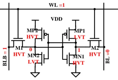
Next on write mode, the worst corner at Global variation is PFNS that makes the cross-couple inverter of 6T cell trip voltage larger than normal. Another reason is pass-gate also NMOS composition that makes the external data transmits slower into cells. We consider the local variation in Fig. 2.33 which is the worst case in write mode. We assume the right-side becomes to write “0” and left-side write “1”, which MN1 and M2 are used high VT that writing trip voltage comes higher. In left side, the MP2 is used high VT and MN2 is low VT that condition let the trip voltage lower. We also show Fig. 2.34 that read operation in the worst VT case.
29 0 1 WL =1 B L B = 1 B L = 0 MP1 LVT MP2 HVT MN1 HVT MN2 LVT M1 HVT M2 HVT VDD 0 1 WL =1 B L B = 1 B L = 1 MP1 LVT MP2 HVT MN1 HVT MN2 LVT M1 LVT M2 LVT VDD
2.8 Modern SRAM Design Methodology
Because the process comes to smaller in recent years, the Global and Local variation, leakage, half selected, and SNM are very critical. To solve these problems and improve the system circuits, today use some design circuit methods or
technological improvements on the process can clear up that.
2.8.1 Dual Supply Voltage
For improving the read/write ability, we can change the cell supply voltage at the appropriate time. If we wish to advance the read ability or RSNM, we can increase the cell supply voltage or come down the cell voltage from ground to negative. Else if we
Fig. 2.33 The effect of local variation in write-mode with worse case
30
want to improve the write ability or WSNM, we can reduce the supply of the cell. In Fig. 2.35 [2.14] which is the Dual-Vcc structure diagram.
Cells fixed at 1.2V in the last level cache (LLC) but cells voltage form 0.7 to 1.2V during operation in the core region that run 0.6V to achieve best energy efficiency in standby mode. The dual-Vcc design enables high-density SRAM than the conventional single-Vcc processor. We also see the Fig. 2.36 [2.14] to realize the cell stability compare at different Vcc and its operation Vmin in different bit densit (Mb/cm2).
Fig. 2.35 Single-Vcc and Dual-Vcc processors [2-14]
(a) (b)
31
In order to reach the goal to changes the cell supply voltage, we have many methods. However, we require second supply voltage that we have to design others power converter, power regulator, and so on. The cost is too expensive so we most of chips use just one supply voltage to generate second supply voltage by circuits.
The above description that the way changes the cell supply voltage to improve the read/write ability. In addition, in the Fig. 2.37 [2.15] the SRAM is used the cross-point 8T SRAM and the lowest supply voltage of the cell is “VSM”.
In read operation, the VSM, which connects to column’s VSS becomes negative bias by the read enable signal (RE). As a result, the enlarged SRAM cell bias improves the static noise margin (SNM). In general, a simple application of the negative VSS technique to the 6T SRAM accompanies with the power increase because all of the cell current in the half-selected columns increases simultaneously. [2.15]
Fig. 2.37 The cross-point 8T SRAM schematic, layout, read/write negative-biased circuit, and waveform [2.15]
32
2.8.2 Negative Bit-Line
At the Fig. 2.37 [2.15], in write operation, the negative-based circuit will pull down the BL voltage to the negative. This method main improve the write ability. Lower bit-line voltage makes the cell written successfully in insufficient write margin. Fig. 2.38 [2.16] shows the circuit and waveform of Constant-Negative-Level Write Buffer. Its working use a negative-bootstrap circuit in a SRAM cell. The bootstrap capacitance and the signal boost-enable running depending on the memory cell count on a bit-line. It means that the charge in C_boost is proportional to each cell bit-line. Besides, the target bias range is -0.15V±0.05V. The design does not be much negative to hold the data in non-chosen cells and writing the data into the select cell shown in Fig. 2.39 [2.16].
33
Fig. 2.40 [2.17] shows that the write drive also use the capacitance “Cboost” to boost the negative voltage. The node “Nboost” connects to eight physical BL pairs, including the upper (Ntu/Ncu) and lower half (Ntl/Ncl) partitions. The Nboost node is per-charged to GND and the WS1n voltage is VDD before into write cycle. As gets into write cycle, WS1n node is pulled down to GND and the Nboost node voltage is turned into a negative voltage instantly in order to achieve bit-line voltage negative. The result (Fig. 2.41 [2.17]) of the designed circuit is worse in high voltage than in low voltage for the effect of negative bit-line.
34
Fig. 2.40 Write driver with boost control [2.17]
35
2.8.3 Dynamic Word-Line Voltage
To control the WL voltage also is the way to improve the read/write ability. As the WL voltage increase, the pass-gate is able to be stronger due to the read/write speed better than original. Nevertheless, in 6T SRAM the read-disturb will raise and RSNM comes into lower. Fig. 2.42 [2.18] shows the RSNM with WL voltage with/without local VT variation. Expressly, the Fig. 2.42(a) verities the argument, which WL voltage lower and the SNM is better in symmetry margin. However, we should consider the variation of VT so the result (Fig. 2.42 (b)) cannot run in lower voltage. In this paper, the WL level should be lowered by more than 20% compared to the supply voltage of 1.0V.
Cause of the WL voltage lower is better in read mode on the 6T SRAM, Fig. 2.43 [2.18-19] shows the read assist circuit (RAC) to control the WL voltage and solve the problem. In the conventional circuitry, which use multiple pull-down NMOS transistors (called replica access transistors, RATs) to reduce the voltage of WL. WL voltage versus VT simulated results for two temperatures we found two problems. The Fig. 2.42 SNM improvement by lowering WL voltage in 6T SRAM in case of (a) with and (b) without local VT variations. [2.18]
36
first problem: in the FS condition, WL voltage drops too much at -40℃ that degrades the operation speed and write margin. The second problem: WL voltage at SS corner, which is the worst condition of the cell current. To solve the problem the paper design another circuit that is proposed circuitry. According to the simulated results the temperature dependence of a resistance is generally smaller than that of MOS transistors.
There is a write assist circuit (WAC) in Fig. 2.44 [2.18-19]. Lowering the voltage level of power line in the memory cell array (ary-VDM) is one of the effective ways of ensuring the SRAM write margin. To enhance the write margin against the increasing variation accompanied by the scaling it is necessary to lower the voltage of ary-VDM immediately. The ary-VDM lowering in several cases of the segment division number (#div=1, 2, 4, 8) and displays the waveform in Fig. 2.45(a) [2.19]. Also shows the DC simulation result of improvement of write ability defined by
Fig. 2.43 Improving read stability depending on process and temperature variations. [2.18-19]
37
write-trip-point in Fig. 2.45(b) [2.19]. We realize the division number larger and the write-trip-point becomes higher to write easily.
Fig. 2.44 Write assist circuit (WAC) improving write stability [2.18-19]
(a) (b)
Fig. 2.45 (a) Simulated waveform of the ary-VDM and dmy-VDM in the write status. (b) Comparison of the write ability by DC simulation result of the write-trip-point. [2.19]
38
2.9 Power Consumption
Due to the thesis designed chip main operates in low voltage, so the power also reduces naturally. The total power is composed of dynamic power, short-circuit power, and static power dissipation. We will in order to discuss these three power dissipations in below description.
2.9.1 Dynamic Power Dissipation
Fig 2.46 [2.20] is a CMOS schematic of inverter. The output currents IDP, IDN, and the load capacitance Cint are the major effect of dynamic power dissipation. Dynamic power dissipation usually defines average power of the period T as VIN signal changes VDD from GND at moment and VIN signal changes GND form VDD transiently.
We drive the average dynamic power dissipation formula like that:
PD = , according to IDN=IDP=IC=C
=
= ] dVo
39 =
= = (2.1)
We get the equation in above derivation; f is represented to the frequency for the input signal. In addition, gates usually do not switch every cycle we have to think the probability of switching. For this reason, we superadd the factor α in the equation 2.1. The final Dynamic power is expressed as:
PD = (2.2)
We can consider the (2.2) equation to realize that dynamic power is proportional to the switch factor, frequency, loading capacitance, and square of supply voltage.
2.9.2 Short-Circuit Power Dissipation
A CMOS inverter working in digital usually turns on only one transistor. If input signal is at high level (VDD), the NMOS transistor conducts, and else if input signal is at low level, which the PMOS will conduct. However, there will be a time period in which both the NMOS and PMOS turn on during a transient on the input. Because of a short-circuit (I) to flow from supply to ground as shown in Fig. 2.47 [2.21] for an inverter without loading.
40
Short-circuit power in general can be expressed as
(2.3) [2.21]
Where is represented to the mean current during a time T, which equals to one period of the input signal. It can be written as
(2.4)
Where τ is the time by input rise and fall time, and β is the gain factor (uA/V2) of a transistor. In the equation, we realize to decrease supply voltage and rise/falling time of input signal that can mitigate the short-circuit power dissipation.
2.9.3 Static Power Dissipation
There is no DC current path for logic device in ideal condition stand-by mode. Nevertheless, there is current on MOS for standby in fact, which main is leakage current. Then, we will introduce major leakage currents of MOSEFT in below description [2.22-23]. Most of leakage can be divided into three parts: gate leakage, sub-threshold leakage, and reverse-bias PN-junction current as shown in Fig. 2.48 [2.22].
41
GATE LEAKAGE
Gate leakage is composed of tunneling into and through gate oxide, injection of hot carriers form substrate to gate oxide, and gate-induced drain leakage (GIDL). At first, we discuss the oxide tunneling current. Today reduction of gate oxide thickness gets to increase the field across the oxide. The high electric field coupled with low oxide thickness makes electrons tunneling from substrate to gate and also from gate to substrate through the gate oxide. [2.23]
The second, we introduce the leakage of hot-carrier injection. Due to high electric field near the Si-SiO2 interface in a short-channel transistor, electrons or holes can gain sufficient energy form the electric field to cross the interface potential barrier and enter in the oxide layer as shown in Fig. 2.49. The effect is known as hot-carrier injection. [2.23]
Final gate leakage is Gate-Induced Drain Leakage (GIDL). As a result of GIDL is high filed effect in the drain junction of an MOS transistor. As the gate is biased to form an accumulation layer at the silicon surface, the silicon surface under the gate has almost same potential as the p-type substrate. Due to presence of accumulated holes at the surface, the surface behaves like a p region more heavily doped than the substrate. This causes the depletion layer at the surface to be much narrower than
42
elsewhere. While the negative gate bias is large shows in Fig. 2.50, the n+ drain region under the gate can be depleted. The condition causes more filed crowding and peak field increase, resulting in a dramatic increase of high field effects. [2.23]
SUBTHRESHOLD LEAKAGE
Subthreshold or weak inversion conduction current between source and drain in an MOS transistor occurs when gate voltage is below VT. Fig. 2.51 shows the variation of minority carrier concentration along the length of the channel for an n-channel MOSFET biased in the weak inversion region. We let the source is grounded, Vg<VT, and the drain to source voltage . For the condition, Vds drops almost entirely across the reverse-biased substrate-drain pn junction. [2.23]
Fig.2.50 As n+ region is depleted or inverted with high negative gate bias, condition of the depletion region near the drain-gate overlap region of an MOS transistor [2.23]
Fig.2.51 Variation of minority carrier concentration in the channel of a MOSFET biased in the weak inversion. [2.23]
43
PN JUNCTION REVERSE-BIAS CURRENT
A reverse-bias pn junction leakage has two main components: one is minority carrier diffusion/drift near the edge of the depletion region; the other is due to electron-hole pair generation in the depletion region of the reverse-biased junction. Pn junction verse-bias leakage is a function of junction area and doping concentration. If both n and p regions are heavily doped, band-to-band tunneling (BTBT) dominates the pn junction leakage. [2.23]
44
Chapter 3
40nm 512Kb Pipeline Low VDD 8T SRAM
3.1 Introduction
To make the chip performance better and cause to the thesis major to reduce the supply voltage, before beginning design the 512Kb-memory, we read some paper to realize and learn the skips to use that. [3.1-10]
As the process is getting smaller and smaller, we started to care about the power eliminate as much as possible to reduce. So, this chip used 8T SRAM is not a conventional single-ended 8T cell (Fig. 3.1(a)) [3.11]. We use the 8T cell with adaptive VVSS control (Fig. 3.1 (b)) [3.12] and add the differential data-aware power supplied above a set of 16-bits 8T cells. Both techniques are able to reduce SRAM active power and leakage power. Moreover, 8T cell with adaptive VVSS control has the same function of non-read-disturb with conventional single-ended 8T cell.
To improve working in higher frequency, we use the concept of pipeline insert to the whole chip. Then, wish for lower VDDMIN, we put into the boosting word-line (WL) scheme in the 512k-bits memory. The function as well as improve write/read ability. However, boosting WL scheme is primarily used improve write ability; read ability just an additional effect. When simulated boosting WL in higher VDD (1.1V), we found the write/read ability to increase the trending less obvious. Inversely, it is more useful at low VDD (0.65V), so designed a voltage detector to control whether turn on WL boosting or not. These above schemes, we will do a careful description in the following article.
45
3.2 8T SRAM Operation
3.2.1 Conventional Single-Ended 8T SRAM
We restart again introduce the conventional 8T SRAM. This 8T cell (Fig. 3.1 (a)) [3.11] adds two-transistors read stack in the conventional 6T cell. The below transistor gate of the stacking-transistor is connected to the node of Q. While write operation, we just turn on the WWL directly and RWL not turn on. Then the working way is the same by the conventional 6T SRAM cell. Afterwards, the read operation is turning on RWL and turning off WWL that the current only through two stack transistors if the Q value is logic “1”, then RBL is pulled down to logic “0”. If Q is logic “0” that RBL voltage is a floating “1”. In addition, the two cross-coupled inverters of 8T SRAM condition is alike standby state so that don’t have read-disturb problem.
(a) (b)
Fig. 3.1(a) A conventional single-ended 8T SRAM cell.[3.11] (b) A disturb-free DAWA single-ended 8T SRAM cell. [3.12]
QB Q W B L B W B L R B L RWL WWL VDD VVDD2 VVDD1 (R)WL QB Q (R )B L W W L B W W L V V S S
46
3.2.2 Disturb-free DAWA Single-Ended 8T SRAM
This 8T cell is used to our chip (Fig.3.1(b)) [3.12]. Due to improve the write-ability, we adjust the PMOS of the cross-coupled inverter to be used High-Vt, another transistors are used regular-Vt. Two internal pass-gates are controlled WWL and WWLB by column-base respectively. The external pass-gate is handled row-base signal (R)WL and the source/drain end is connect to (R)BL, the other end is linked to internal pass-gate. The VVDD1 and VVDD2 are controlled by DAWA we next section will tell them.
Because we use the 8T SRAM cell design the chip, we will realize the 8T SRAM basic operation in detail. In stand-by mode, the WWL, WWLB, and (R)WL don’t turn on. We set the VVSS is logic 0 and (R)BL is logic “1”, as shown in Fig. 3.2(a). The stand-by mode major purpose is pre-charge the (R) BL.
In read mode, the WWL and WWLB also don’t turn on that can improve the Read Static Noise Margin (RSNM). Moreover, the VVSS is set logic “0” and the (R)WL turn on let the (R)BL floating. If the QB is logic “0”, then the NMOS connect by the VVSS don’t turn on that the (R)BL is going to floating “1”. On the other hand, the QB is logic “1”, the same NMOS change to switch on that the (R)BL discharge to the floating “0”, as shown in Fig. 3.2(b). We just pass through two transistors to get the read data.
In write mode, we use the basis of node Q to write 1 or write “0”. While write “1”, it means the Q node data will change from “0” to “1”. The same write-mode operation is turning on the (R)WL and discharging the (R)BL to the logic “0”. Supposing write “1”, WWL switch on and WWLB switch off. VVSS become logic “1”, and then the discharging path is shown in Fig. 3.2(c). If write “0”, WWL turn on and WWLB turn off, VVSS become logic “0” that the path of discharging as shown in Fig. 3.2(d).
47
Fig. 3.3 is the disturb-free new single-ended 8T cell layout. We place the WWL and WWLB between two gates in row-based from original 6T cell layout. There are three row gates at right-side and left-side. The middle layout don’t change that stand for two cross-couple inverters. The 8T SRAM cell layout length is 1.44um and width is 0.59um. So the cell size is 1.44*0.59=0.85um2 in UMC 40nm LP CMOS process.
VVDD2 VVDD1 (R)WL QB Q (R )B L W W L B W W L V V S S (a) (b) VVDD2 VVDD1 (R)WL QB Q (R )B L W W L B W W L V V S S VVDD2 VVDD1 (R)WL QB Q (R )B L W W L B W W L V V S S (c) (d) VVDD2 VVDD1 (R)WL QB Q (R )B L W W L B W W L V V S S
Fig. 3.2 (a) The operation for stand-by mode. (b) The read-mode operation. (c) The operation for wirte-1 mode. (d) The operation for write-0 mode.
48
Finally, we summarize the new 8T SRAM operation in the table 3.1. There are shown three modes at standby, write, and read conditions. The operation is worth noting that the (R)BL is floating in the read state.
mode Standby Write 0 Write 1 Read
(R)WL 0 1 1 1
WWL 0 0 1 0
WWLB 0 1 0 0
VVSS 0 0 1 0
RBL 1 0 0 floating
Fig.3.3 Cell layout for disturb-free DAWA single-ended 8T SRAM
![Fig. 2.5 Multi-fin FinFET structure [2.3]](https://thumb-ap.123doks.com/thumbv2/9libinfo/7494384.115688/21.892.149.751.518.1027/fig-multi-fin-finfet-structure.webp)
![Fig. 2.6 TG-FinFET 6T SRAM cells schematic [2.4]](https://thumb-ap.123doks.com/thumbv2/9libinfo/7494384.115688/22.892.146.758.503.1020/fig-tg-finfet-t-sram-cells-schematic.webp)
![Fig. 2.7 TG-FinFET 6T SRAM cells layout [2.4]](https://thumb-ap.123doks.com/thumbv2/9libinfo/7494384.115688/23.892.166.671.143.446/fig-tg-finfet-t-sram-cells-layout.webp)