國立交通大學
電信工程學系
碩
士 論 文
應用於 Millimeter Wave 射頻接收機之 CMOS 低雜訊
放大器與 CMOS 降頻器設計研究
Design of CMOS LNA and CMOS Down-Converting Mixer for
Millimeter Wave Receiver
研 究 生:江沛遠
指導教授:周復芳 博士
應用於 Millimeter Wave 射頻接收機之 CMOS 低雜訊放大器與
CMOS 降頻器設計研究
Design of CMOS LNA and CMOS Down-Converting Mixer for
Millimeter Wave Receiver
研 究 生:江沛遠 Student: Pei-Yuan Chiang
指導教授:周復芳 Advisor: Christina F. Jou
國 立 交 通 大 學
電 信 工 程 學 系 碩 士 班
碩 士 論 文
A thesis
Submitted to Department of Communication Engineering College of Electrical and Computer Engineering
National Chiao Tung University In Partial Fulfillment of the Requirements
for the Degree of Master of Science in Communication Engineering
June 2008
Hsinchu, Taiwan, Republic of China
應用於 Millimeter Wave 射頻接收機之 CMOS 低雜訊放大器
與 CMOS 降頻器設計研究
研究生:江沛遠 指導教授:周復芳 博士
國立交通大學電信工程學系碩士班
摘 要
本論文主要探討在 Millimeter Wave 接收機中兩個重要的高頻電路,一個 是超寬頻低雜訊放大器,另一個是超寬頻降頻器。分別在第一部分與第二部份對 該兩電路做分析研究。 第一部份:提出利用電晶體本身的寄生電容與 transformer 回授的寬頻低 雜訊放大器,主要應用頻段在 10~18 GHz。該低雜訊放大器藉由在輸入端電晶體 加入 transformer,利用 transformer 本身的回授機制與電晶體的寄生電容,能 夠在 10~18 GHz 頻寬內達到輸入阻抗低於-12dB 以下,同時放大器的雜訊指數低 於 3.5dB。由於在輸入端並無增加任何元件來做輸入阻抗匹配,因此該放大器能 夠有較低雜訊指數的表現。此放大器是使用 TSMC 0.18μm mixed signal/RF process,在 1.8V 電壓下,能提供 17dB 的增益、最低雜訊指數為 2.4dB、-22.6dBm 的線性度(IIP3)、功率消耗為 37.6mW(緩衝級不算在內)。 第二部份:設計一個應用於 W-Band 接收機的降頻器,首先會先簡單介紹此 W-Band 接收機的系統架構,之後將提出所設計的寬頻降頻器。該降頻器輸入頻 段為 8.7~17.4 GHz,利用 LO 訊號為 17.5 GHz,將此頻段的訊號降頻到 0.1~8.8GHz(IF 端)。該降頻器有將近 10 GHz 的 IF 頻寬,Conversion Gain 7dB,線性
度大於 8dBm(IIP3)。此外該降頻器會使用到兩個 Balun,分別將 RF 和 LO 訊號分
成差動訊號,因此在降頻器中加入兩個 on chip 的 Balun,並且將對 Balun 做探
討。同時因為 IF 端有將近 10 GHz 的頻寬(單端輸出),所以必須設計寬頻且高
CMRR 的 IF 端電路。該 IF 端電路有 25dB 以上的 CMRR 在 0.1~8 GHz 頻段內。
Design of CMOS LNA and CMOS Down-Converting Mixer for
Millimeter Wave Receiver
Student: Pei-Yuan Chiang Advisor: Dr. Christina F. Jou
Department of Communication Engineering
National Chiao Tung University
ABSTRACT
This thesis discusses two high frequency circuits applied in millimeter wave
receiver. One is an ultra wide band low noise amplifier and the other is a wide band
down-converter. The two circuits will be analyzed in the following two parts.
In part one, a wide-band (10~18GHz) low noise amplifier (LNA) is proposed. With
transformer feedback in the traditional cascode amplifier, good input matching is
achieved from 10 GHz to 18 GHz. The noise figure is below 3.5dB over 10-18GHz.
There are no additional input-matching elements in the input gate of the cascode
amplifier, so that the LNA can achieve lower NF. The LNA is designed based on
CMOS TSMC 0.18μm mixed signal/RF process. With 1.8V supply voltage and three
stage amplifiers to achieve wider gain bandwidth, the LNA can achieve
input-matching of -12dB over the bandwidth; minimum NF 2.4dB; gain (S21) of
17dB and 1dB gain compression (P1dB) at -22.6dBm. The power consumption is
37.6mW (exclude buffer)
In part two, a wide band down converter will be designed for W-band receiver.
First a W-band receiver architecture will be introduced and one of the down-converter
in the receiver will be proposed. This part describes the development of the
down-converter, with the RF frequency chosen to be 8.7~17.4 GHz, LO fix at 17.5
GHz and IF close to DC~8.7 GHz. The down converter can achieve about 10 GHz IF
bandwidth、Conversion Gain 12dB and IIP3 above 8dBm. There will be two on-chip
baluns implemented in the circuit for converting single RF and LO signals to
differential signals and the balun will be discussed. Besides the down-converter has
10 GHz IF-bandwidth, the IF stage circuit must provide high CMRR over the
bandwidth. In the proposed circuit the IF stage can achieve above 25dB CMRR in
0.1~8 GHz.
誌 謝
首先我要感謝我的指導教授周復芳以及胡樹 兩位老師,由於他們的悉心 指導和不時的討論並指點我正確的方向,讓我在 RF 領域能有效率的學習成長並 獲益匪淺,老師對學問的嚴謹更是我輩學習的典範。另外感謝實驗室的所有夥 伴,因為有你們陪伴我的碩士生活,使我在學習成長的路上不曾感到孤單。最後 我要感謝我最愛的父母親,在求學的路上給予我最大的支持和包容,讓我能順利 地完成碩士學業。在此僅以小小的研究成果貢獻給我家人,並與你們分享我的喜 悅。 VCONTENTS
Chinese Abstract I
English Abstract Ш
Acknowledgement V
Contents VI
List of Tables VII
List of Figures VIII
Chapter 1
Introduction
………...……..1
1.1 Introduction... 1
-1.2 Thesis organization ... - 3 -
Chapter 2
Transformer Feedback CMOS Low Noise Amplifier…... 4
-2.1 Introduction... - 4 -
2.2 Circuit Analysis... - 5 -
2.3 Simulated Results... ………..- 8 -
2.4 Conclusion ... 11
2.5 Reference………-12-
Chapter 3 Down-Converting Mixer for Millimeter Wave
Application ………..- 13 -
3.1 Introduction... - 13 -
3.2 Wide IF bandwidth Downconverting Mixer Design ... 18
-A. Input RF Citcuit Design... 18
-B. Mixering Circuit Design ... 28
C. Output IF Circuit Design………...-30-
3.3 Simulated and Measured Results... 36
A. Marchand Balun………...- 36 -
B. Mixer-A………....- 41 -
C. Mixer-B ………...- 50 -
3.4 Reference………..- 54 -
Chapter 4
Conclusion and Future Work………... 57
-4.1 Conclusion and Feture Work... 57
4.2 Reference……….. 59
LIST
of
TABLE
Table 3-12 A simulation result summary table of the proposed Marchand
balun………...………..32
Table 3-22 Comparison of Simulated and Measured Results………...…...47
Table 3-34 Comparison of Mixer-A’s simulated and measured
results……….………..56
Table 3-42 The summary of Mixer-B……….………60
L
IST
of F
IGURE
Fig. 1-1. Schematic of the RF and IF circuits in the wide-band receiver……….. 2
Fig. 2-1. Proposed LNA schematic……… 2
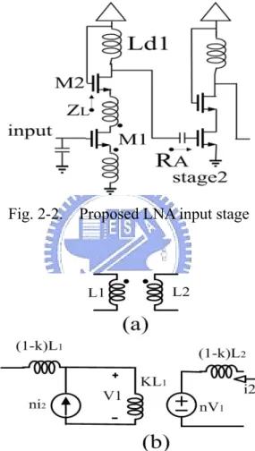
Fig. 2-2. Proposed LNA input stage……….. 6
Fig. 2-3. (a) Transformer (b) Equivalent circuit of transformer……… 6
Fig. 2-4. Input matching small signal circuit………. 7
Fig. 2-5. Simplified input matching mechanism………... 7
Fig. 2-6. S11 of the proposed LNA………... 8
Fig. 2-7. Post-simulated S11 versus frequency………. 8
Fig. 2-8. Post-simulated S21 versus frequency………. 9
Fig. 2-9. Post-simulated S22 versus frequency………. 9
Fig.2-10. Simulated NF versus frequency……….. 9
Fig.2-11. P1dB for 15GHz………. 10
Fig.2-12. Proposed LNA layout……….. 10
Fig. 3-1. The basic operation of the mixer……….... 13
Fig. 3-2. The schematic is a typical double balanced mixer with the dotted line current source for current injecting method……… 15
Fig. 3-3. Schematic of the wide-band receiver……….. 17
Fig. 3-4. Distribution of the four IF bands with fLO = 8.7GHz. The DC - 4fLO frequency range will be divided into 4 bands………. 17
Fig. 3-5. Simulated S-parameters of the transistor……… 18
Fig. 3-6. Different circuit configurations used to convert the single-ended RF signal into the differential-mode RF signal at RFdiff………. 20
Fig. 3-7. Input RF circuit schematic……….. 21
Fig. 3-8. Spiral inductor under test……… 22
Fig. 3-9. Spiral broadside-coupled Marchand coupler……….. 24
Fig.3-10. Spiral Marchand balun where the input port 1 is connected to the edge of the spiral while the output ports are extracted from the center of each spiral………... 24
Fig.3-11. The simulated output magnitude and phase difference of the Marchand balun……….. 25
Fig.3-13. The simulated input reflection coefficient of the Marchand balun with tapered ground……… 27
Fig.3-14. Mixing circuit with LO injection……… 29
Fig.3-15. Revised mixing circuit……… 29
Fig.3-16. The equivalent small-signal circuit of two transistor in cascade for low-frequency common mode rejection………. 31
Fig.3-17. Output IF circuit. Each transistor's gate biasing sub-circuit is
omitted……….. 32
Fig.3-18. CMRR of the IF output stage………... 34
Fig.3-19. The differential-mode and common-mode voltage gain of the three different IF output-stage circuits………. 35
Fig.3-20. The modified mixer’s output stage for better linearity………. 36
Fig.3-21. The proposed Balun-A……….. 37
Fig.3-22(a). Magnitude error of Balun-A………. 38
Fig.3-22(b). Phase error of Balun-A………. 39
Fig.3-22(c). Return loss of Balun-A………. 39
Fig.3-22(d). Insertion loss of Balun-A……….. 40
Fig.3-23 The schematic of Mixer-A……… 41
Fig.3-24. The schematic of LC balun………... 41
Fig.3-25(a). The layout of Mixer-A……….. 42
Fig.3-25(b) The chip die photograph………... 43
Fig.3-26. Arrangement of DC and RF probes……….. 44
Fig.3-27. The measured arrangement of S-parameter……….. 44
Fig.3-28. The measured arrangement of conversion gain……… 44
Fig.3-29. The measured arrangement of IIP3……….. 45
Fig.3-30(a) RF Port return loss for RF signal from 8.5~17GHz………. 46
Fig.3-30(b). LO port return loss for a fixed LO frequency 17.5GHz…………... 46
Fig.3-30(c). IF port return loss for IF frequency 0.5~9GHz……… 47
Fig.3-31. Conversion gain of Mixer-A whit LO at 17.5GHz………... 47
Fig.3-32. Isolation of Mixer-A………. 48
Fig.3-33(a)~(c) IIP3 of Mixer-A……… 48
Fig.3-35. The schematic of Mixer-B……… 50
Fig. 3-36. The layout of Mixer-B……….. 50
Fig. 3-37. RF port return loss for RF signal band 8.5~17GHz………. 51
Fig. 3-38. LO port return loss for a fixed LO frequency at 17.5GHz………... 51
Fig. 3-39. IF port return loss for IF band 0.5~9GHz………. 52
Fig. 3-40. Conversion gain versus RF frequency with LO at 17.5GHz……… 52
Fig. 3-41. Isolation of RF port to IF port……….. 53
Chapter 1
Introduction
1.1 Introduction
A wide-band receiver is constructed where its radio frequency (RF) covers
78.3.113.1GHz and its intermediate frequency (IF) bandwidth is set to 34.8GHz.
Instantaneous detection of the intended radio-astronomical spectra is therefore
ensured with this maximized IF bandwidth, thus allows the exploration of the
anisotropy of the cosmic microwave background radiation (CMBR) in the
millimeter-wave frequency range; or more specifically, the inverse-Compton
scattering of the photons by hot electrons in the galaxy clusters, also known as
Sunyaev-Zel'dovich (SZ) effect.
As shown in Fig. 1-1, the incoming signal is first fed into two cryogenic amplifier
modules with each has 70.90Kelvin noise temperature and 20dB gain at 20Kelvin
ambience. To ensure stability, cryogenic isolators have been incorporated into these
amplifiers. The cryogenic WiseWave-FDB1001 mixer made by WiseWave
Technologies (now Ducomun Technologies) is then used to down-convert, with 5.7dB
conversion loss, the signal to (quasi) DC.34.8GHz. Of course, it is possible using a
room-temperature mixer instead, but that will require the precision insertion of a
hermetically-sealed millimeter-wave waveguide between the front-end cryogenic
amplifier and this room-temperature mixer, and the attenuation along this long
wavequide will also be pronounced. Four separate bands can now be extracted by the
use of amplifiers, filters, and another three mixers, each with 8.7GHz IF bandwidth
and the LO frequency is fixed at 17.6GHz, 17.6GHz and 26.3GHz, respectively. The
reason for not using an 8.7GHz LO for down-converting in the second band is
because this LO is bordering the IF band, thus any residual LO at IF output is hard to
remove; by contrast, a 17.4GHz LO can be easily taken off afterward.
Fig. 1-1. Schematic of the RF and IF circuits in the wide-band receiver. With fLO =
8.7GHz, the incoming 78.3.113.1GHz signal will be amplified and down-converted
onto DC.34.8GHz, which is split into four separate bands of equal bandwidth, as
indicated by the shaded areas.
1.2 Thesis Organization
This thesis contains mainly two circuits; one is low noise amplifier and the other is
wide IF bandwidth mixer, which will be discussed in chapter2 and chapter3
respectively. In each chapter the circuit will be introduced and then analyzed. For
clearly analyzing, dividing the circuit into smaller block and analyzing blocks step by
step is adopted. In the following of each chapter, simulated and measured results will
be presented.
In chapter2 is the low noise amplifier designed by CMOS TSMC 0.18μm mixed
signal/RF process. With the transformer feedback in the input, the input impedance
can be achieve -12dB for 10~18GHz. Due to the feedback loop of transformer and
transistor’s parasitic capacitor, no additional elements needed for input matching.
Thus in this schematic the noise of the input port is only from the gate noise of the
input transistor. The simulated results shows the LNA has 17dB gain (S21) and 3.5dB
NF for 10~18GHz with 37.6mW power consumption.
In chapter3 is the wide IF bandwidth down-converting mixer. The mixer is
designed within two on-chip baluns, and thus Marchand Balun will be first introduced.
Then the proposed wideband mixer will be shown and analyzed. The mixer has 7dB
conversion gain and 9GHz IF bandwidth.
In Chapter4 are the short conclusions of the two circuits (LNA, mixer). The
drawbacks of the circuits will be pointed out and some unexplained phenomenon will
be shown. Those unexplained problems are the aim of future work.
Chapter 2
Transformer Feedback CMOS Low
Noise Amplifier
2.1 Introduction
Wide-band communication system (like UWB for 3.1 to 10GHz; 57 to 64GHz
millimeter wave system) have received much attention due to high data rate and high
speed communication. In such a wideband system, LNA is in the first stage after
antenna in the front-end receiver block. To interface with the antenna and the
preselect filter, LNA requires input match to 50Ω over the bandwidth. Meanwhile
LNA must provide high gain and the most important, low noise.
Several typologies have been proposed for wideband input matching. (a) distributed
amplifier[1]:distributed amplifier (DA) can achieve much wider input matching by
several stages of amplifier. However, DA has gain problem due to long transmission
line loss and consumes more power and chip area. It is unsuitable for modern
wideband system. (b) negative feedback amplifier[2]: negative feedback amplifier can
achieve wideband matching due to parasitic capacitance. This configuration doesn’t
provide high gain and may has stable problem. (c) common gate configuration:
common gate configuration[3] has good linearity and wideband input matching. Due
to the simplicity of common gate input-matching mechanism, it has low noise but
smaller gain than common source amplifier. (d) filter configuration[4]: With inductors
and capacitances in the input of degenerated common source amplifier, it forms a
Chebyshev filter structure in the input. The input matching bandwidth is dependent on
the order of Chebyshev filter. Therefore it can achieve wider input matching but the
noise figure is degraded by the imperfect effect of inductors and capacitances.
Fig. 2-1. Proposed LNA schematic
In this chapter, a LNA designed in CMOS TSMC 0.18μm mixed signal/RF process
is proposed. The LNA has no additional input tuning circuits for lower noise. Input
matching is achieved due to parasitic capacitance (Cgd, Cgs) and transformer
feedback. The design consideration is analyzed, followed by the post-simulated
results and the conclusion.
2.2 Circuit Analysis
The architecture of proposed LNA is shown in Fig. 2-1. By cascading two stages
(stage2 and stage3) to amplify signal, the LNA can achieve enough gain above 10
GHz. The output buffer is implemented for 50Ω output-matching. For input matching
analysis, ZA in Fig. 2-2 can be approximated as a resistor RA at high frequency.
Looking into common gate transistor M2, the impedance ZL is [3]
( ) ( ) 1 2 1 1 2 2 ( ) 2 2 2 ( ) 2 2 ( ) ( ) ( ) (1 ) Z L g m X o R o g m R o g m j X o X s R o X o R o X o R j X ω ω ω ω ω ω ω = ⎛ ⋅ − ⎞ ⎛ + ⎞ ⎜ − ⎟− ⎜⎜ + ⋅ ⎟⎟ ⎜ + ⎟ ⎝ + ⎠ ⎝ ⎠ = + L L L
where Ro is the output resistor of M2
1 ( ) 2 X s C gs ω ω − = ( ) ( ) 1 // // 1 2 Zo jXo RA j Ld j Cgd ω ω ω ω = =
The impedance ZL is close to 50Ω over the bandwidth due to the common gate
typology of transistor M2. it can be assumed that ZL is 50Ω for simplified calculation.
A transformer model [5] is shown in Fig. 3 where L1=0.5nH, L2=1nH, k=0.6, n=2
in proposed LNA.
Fig. 2-2. Proposed LNA input stage
Fig. 2-3. (a) Transformer (b) Equivalent circuit of transformer
By replacing the transformer equivalent circuit into Fig. 2-2, the input matching
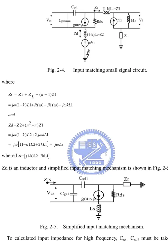
small signal circuit is shown in Fig. 2-4.
Fig. 2-4. Input matching small signal circuit. where
[
]
3 ( 1) 1 (1 ) 1 ( ) ( ) 1 2 2 ( ) 1 (1 ) 2 2 1 (1 ) 2 2 1 Zr Z Z n Z L j k L R jX j kL and Zd Z n n Z j k L j kL j k L kL j Ls ω ω ω ω ω ω ω = + − − = − + + − = + − = − + = − + = ω where Ls=[(1-k)L2+2kL1]Zd is an inductor and simplified input matching mechanism is shown in Fig. 2-5.
Fig. 2-5. Simplified input matching mechanism.
To calculated input impedance for high frequency, Cgs1、Cgd1 must be taken into
account[6] and the S11 smith chart is shown in Fig. 2-6.
Fig. 2-6. S11 of proposed LNA.
Due to the transformer feedback and the parasitic capacitance, the real part of
S11 in Fig. 2-6 is close to 50 Ω over 10~18GHz. Meanwhile the circuit has low NF
because only the parasitic capacitance in the gate of M1.
2.3 Simulated results
This section presented the post-simulated results of the proposed LNA operating
over 10-18GHz under typical-typical corner with a supply voltage of 1.8V. This work
is designed and simulated using TSMC 0.18µm mixed signal/RF CMOS 1P6M
technology. The transformer and inductors in the circuit is verified by EM-simulation
(ADS momentum).
Fig. 2-7. Post-simulated S11 versus frequency.
Fig. 2-8. Post-simulated S21 versus frequency.
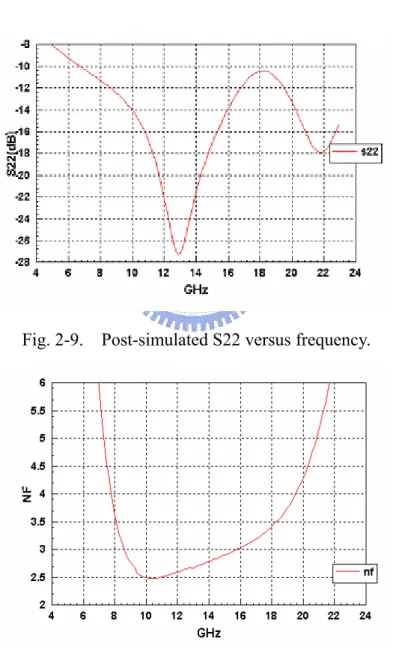
Fig. 2-9. Post-simulated S22 versus frequency.
Fig. 2-10. Simulated NF versus frequency.
Fig. 2-11. P1dB for 15GHz.
The S-parameter is shown in Fig. 2-7, Fig. 2-8, and Fig. 2-9 where S11 in Fig.
2-7 < -15dB over 11~17GHz. The gain (S21) in Fig. 2-8 is 17dB from 10 to 18GHz
with variation less than 1dB. S22 in Fig. 2-9 is less than -10dB over 10~18GHz. The
transistor’s size and the transformer must be fine tuned to provide a good input
impedance matching and low noise. The simulated noise figure is shown in Fig. 2-10.
In Fig. 2-10, it has been shown that the minimum NF is 2.5dB at 10GHz, and increase
to 3.4dB at 18GHz. The P1dB in Fig. 2-11 is -22.6dBm for 15GHz. The total power
consumption is 37.6mW.
The layout of the LNA is shown in Fig. 2-12. The chip area is 1mm by 0.8mm.
Fig. 2-12. Proposed LNA layout. 1mm X 0.8mm
2.4 Conclusion
In this paper, a novel wide bandwidth LNA is proposed based on CMOS TSMC
0.18μm mixed signal/RF process. Only by parasitic capacitance and transformer
feedback, it can achieve input matching over 10~18GHz. And due to the simplicity of
the wideband input matching mechanism, very low noise can be achieved from
10~18GHz.
2.5 Reference
[1] Sullivan, P.J.; Xavier, B.A.; Ku, W.H,“An integrated CMOS distributed amplifier
utilizing packaging inductance”, Microwave Theory and Techniques, IEEE
Transactionson Volume 45, Issue 10, Part 2, Oct. 1997 Page(s):1969 - 1976
[2] Shih-Chih Chen; Ruey-Lue Wang; Ming-Lung Kung; Hsiang-Chen Kuo, “An
Integrated CMOS Low Noise Amplifier for 3-5 GHz UWB Applications”
Electron Devices and Solid-State Circuits, 2005 IEEE Conference on 19-21 Dec.
2005 Page(s):225 - 228
[3] Yang Lu; Kiat Seng Yeo; Cabuk, A.; Jianguo Ma; Manh Anh Do; Zhenghao Lu,”
A novel CMOS low-noise amplifier design for 3.1-to 10.6-GHz ultra-wide-band
wireless receivers” Circuits and Systems I: Regular Papers, IEEE Transactions on
[see also Circuits and Systems I: Fundamental Theory and Applications, IEEE
Transactions on]Volume 53, Issue 8, Aug. 2006 Page(s):1683 - 1692
[4] Andrea Bevilacqua, and Ali M. Niknejad, “An Ultrawideband CMOS Low-Noise
Amplifier for 3.1–10.6-GHz Wireless Receivers,” IEEE JOURNAL OF
SOLID-STATE CIRCUITS, VOL. 39, NO. 12, DECEMBER 2004
[5] Long, J.R,” Monolithic transformers for silicon RF IC design”, Solid-State
Circuits, IEEE Journal of Volume 35, Issue 9, Sept. 2000 Page(s):1368 - 1382
[6] Hu, R.,” Wide-band matched LNA design using transistor's intrinsic gate-drain
capacitor”, Microwave Theory and Techniques, IEEE Transactions on Volume 54,
Issue 3, March 2006 Page(s):1277 - 1286
Chapter 3
Down-Converting Mixer for Millimeter
Wave Applications
3.1 Introduction
To transform the radio-frequency (RF) signal to a much lower intermediate
frequency (IF), down-converter mixer is to be used. For example, in the IEEE802.11
a/b/g receiver, the 2.45GHz incoming RF signal will be down-converted by mixers to
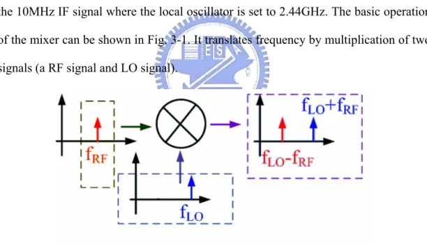
the 10MHz IF signal where the local oscillator is set to 2.44GHz. The basic operation
of the mixer can be shown in Fig. 3-1. It translates frequency by multiplication of two
signals (a RF signal and LO signal).
Fig. 3-1. The basic operation of the mixer.
Although there are many topologies of mixers (single balanced、double balanced、
triple balanced… ), the double balanced circuit configuration have been readily
appearing in microwave and millimeter wave applications for it’s good isolations.
However, not all the technology developed in double balanced circuit configuration
for further improving the mixer’s performance, at low frequency or even a few GHz,
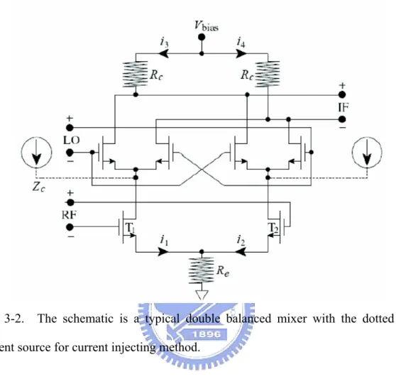
are applicable at tens of GHz. For example as indicated in Fig. 3-2, the schematic is a
typical double balanced mixer (excluding the dotted line current sources). In order to
enhance the conversion gain, it is perhaps to use large Rc. However as Rc increasing,
the voltage drop between Rc will also increasing, driving out of the original bias
condition. Increasing the power supply voltage Vbias is a solution but it will consume
more power. The alternated solution is externally injecting current by using the two
current sources as indicated in Fig. 3-2. However this solution can’t be applied at tens
of GHz, since the current are usually made of p-type transistors, the output impedance
of the current source Zc tend to decrease at high frequency and thus deteriorated the
mixer’s performance at high frequency.
The challenge in designing a well-performing microwave or millimeter-wave mixer
is even obvious when considering another factor: IF bandwidth. So far, most of the
mixers with normal-biased transistors, as contrast to resistive transistors with no drain
to source bias, have their wide-band proclamation illustrated by shifting the LO across
the intended RF bandwidth, while keeping the IF band-width comparatively small, i.e.,
wide RF-bandwidth but narrow IF-bandwidth. With an IF bandwidth of hundreds of
MHz, a large output signal voltage can be easily achieved by replacing each Rc in Fig.
3-2 with an appropriate p-type transistor as a active load, for which is capable of
providing a large impedance at low frequency. However, when the IF bandwidth is
extended to several GHz, the rapidly decreasing impedance of this active p-type load
becomes a liability, as it leads to a large variation of the conversion gain over the
intended bandwidth: extremely high impedance at the low-end of the IF frequency
range while at high-end it is mediocre or no better than that of mixers using Rc.
Likewise, the use of extra current source and large Rc for 10.20dB conversion gain
will lose its appeals as IF bandwidth increases, because the IF voltage is now mainly
determined by the much lower input impedance of the following stage rather than Rc
itself.
Fig. 3-2. The schematic is a typical double balanced mixer with the dotted line
current source for current injecting method.
Fig. 3-3 is the schematic of a millimeter-wave receiver which will be used in the
form of array for the determination of the anisotropy of the cosmic microwave
background radiation, and it demands the employment of several wide IF bandwidth
mixers. As indicated by the number inside the crossed circle, the first mixer will
down-convert the amplified 78.3 - 113.1GHz signal to DC - 34.8GHz, or more
precisely, 0.2 - 34.8GHz. Four bands are then separated using amplifiers, filters and
another three mixers, with each has the same IF bandwidth of 8.7GHz; the LO
frequencies are fixed at 17.6GHz, 17.6GHz and 26.3GHz for equal bandwidth
partition. Though the commercial Marki M1R0920, Hittite HMC292 and HMC329
can be used for mixers 2, 3 and 4, respectively, their conversion losses require the
adjacent amplifiers inside and outside module to be very high-gain. Besides, these
passive mixers' poor impedance matching at RF, LO and IF ports inevitably
contribute to the rippled responses versus frequency in their corresponding bands. The
existing system's shortcomings therefore prompt us to design the wide IF-bandwidth
down-converting mixers with matched ports, low noise temperature, positive over-all
conversion gain and, most important of all, a clear IF output spectrum. In this paper,
we intend to focus on the second mixer, which has its input frequency range being 8.7
- 17.4GHz and LO set to 17.4GHz, as shown in Fig. 3-4. The reason why not using a
8.7GHz LO to down-convert the RF is because this LO is bordering the IF band, thus
any residual LO at IF output is hard to remove; by contrast, a 17.4GHz LO will not
have this problem.
Fig. 3-3. Schematic of the wide-band receiver. With fLO= 8.7GHz, the incoming
78.3 - 113.1GHz signal will first be amplified and then down converted into DC to
34.8GHz, which will be further split into four separate bands of equal bandwidth. The
front-end amplifier and mixer are located inside the cryostat from sensitivity
consideration, while the rest are at room temperature.
Fig. 3-4. Distribution of the four IF bands with fLO = 8.7GHz. The DC - 4fLO
frequency range will be divided into 4 bands. The first band can be extracted using a
low-pass filter while the second, third and forth bands have to be down-converted first
using mixers with their LO frequency set to 2fLO, 2fLO and 3fLO, respectively.
3.2 Wide IF Bandwidth Down-Converting Mixer
Design
A. Input RF circuit design
In designing the RF input circuit, the transistors’ size must be chosen properly.
Since the RF incoming signal at frequency 8.7~17.4GHz, the transistor must provide
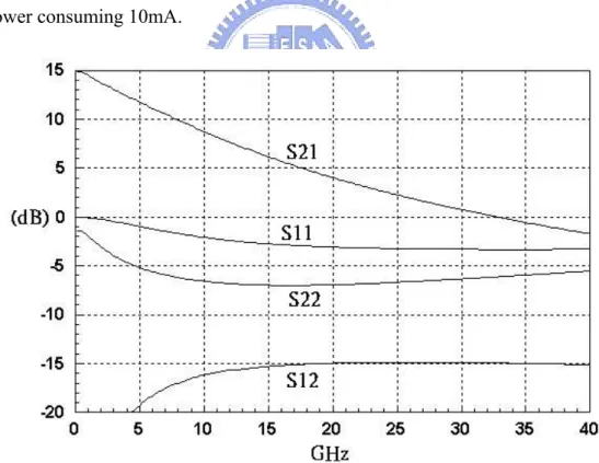
enough gain (S21) and acceptable power consumption at such high frequency. Fig.
3-5 shows the simulated transistor’s S-parameter with TSMC 0.18um RF-CMOS
processing ADS design kit. The curves in Fig. 3-5 are with transistor’s size W=160um
VDS=1.16V, VGS=0.7V, and Id=8.67mA; the S21 is about 7dB in RF bandwidth, and
the power consuming 10mA.
Fig. 3-5. Simulated S-parameters of the transistor. The solid lines are from the large
transistor biased at Vds = 1.16Volt, Vg = 0.7Volt, and Id = 8.67mA;
In order to have better LO-IF isolation, the mixer will be designed in double balanced Gilbert cell topology. This topology requires two differential signals (LO、
RF). While designing RF circuit converting single-ended RF signal to
differential-mode is a challenge especially at high RF frequency. Granted, there are
many circuit configurations available for converting the single-ended RF signal to
differential-mode, and one is the differential pair with one input port grounded, as
shown in Fig. 3-6. However this configuration will cause two problems as follows.
One is that if RF signal is presented at one transistor’s and the other transistor’s gate
is grounded, the RF signal will be at RFdiff in two paths; one is a common-source path,
the other is common-drain and common-gate path. Due to the parasitic capacitors, the
two paths are physically asymmetric and the balanced performance of the RF
differential-mode signal is worse than passive Marchand balun. The other problem is
RF-to-IF isolation. If a 3GHz out of band signal is presented, this configuration will
provide about 7 dB gain and pump the signal to mixer. Amplifying out of band signals
will degrade RF-to-IF isolation and burden the filter before the mixer. On the other
hand Marchand balun has signal degradation of -20dB at low frequency which is
capable of rejecting lower out of band signal.
Lastly, conversion gain degradation notwithstanding, differential-mode signal can
indeed be extracted from the drain and source nodes of the transistor, as indicated by
arrow 2 where the capacitor Cp is for high frequency phase compensation. With good
common-mode suppression for the fundamental frequencies, if two signals 9GHz and
11GHz are presented in transistor’s gate, the two signals on Vα will mostly be
differential-mode; however, the 2GHz and 20GHz signals (due to the nonlinearity of
the first transistor) at Vα are mostly common-mode. When the nonlinearity of the
differential-pair transistors comes to play, differential-mode 7GHz (9GHz minus
2GHz), 9GHz (20GHz minus 11GHz), 13GHz (9GHz plus 2GHz), and 31GHz
(20GHz plus 11GHz) signals all appear at RFdiff. Since the IF bandwidth is 8.7GHz,
the unintended signals thus disturb the output spectrum.
Fig. 3-6. Different circuit configurations used to convert the single-ended RF signal
into the differential-mode RF signal at RFdiff. Perfect differential-mode LO and idea
IF balun are assumed in analyzing these two different conversion approaches.
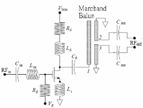
Fig. 3-7. Input RF circuit schematic. The transistor has five 32um-long gate fingers
and is biased at Vd = 1.16Volt, Vg = 0.7Volt, and Id = 8.67mA. The Marchand balun is
used to provide a differential-mode RFdiff.
To minimize all the lower out of band signals and unwanted differential-mode
signals and their harmonics at RFdiff, a distributed Marchand balun is adopted in
designing this mixer's RF circuit, as shown in Fig. 3-7. Granted, there are other types
of passive baluns that can be used; however, their stated merits are mainly for
applications of a few GHz [6], [7]. Distributed Marchand balun made of coupled lines,
on the other hand, has been proved applicable at much higher frequency [8].
Neglecting its loss, an ideal Marchand balun have its S-parameters expressed as
[ ]
0
/ 2
/
/ 2
1/2
1/2
/ 2 1/2
1/2
balunj
j
S
j
j
2
⎡
−
⎤
⎢
⎥
=⎢
⎥
⎢
⎥
−
⎢
⎥
⎣
⎦
where the frequency-dependent coupling factor is set to be -4.8dB. Therefore, port 1,
as indicated by the number in the figure, is matched while the output signals on ports
2 and 3 are 180 degrees out of phase in this ideal case [9], [10]. As the balun will
indeed be fabricated on the lossy silicon substrate, this RF front-end loss will greatly
affecting this mixer's noise performance. Even worse, with capacitive loading the
balun's input impedance can be anything but 50Ω. A one-stage transistor circuit is
then added in front of this balun for wide-band input matching [5].
As this input RF circuit operates at 8.7 to 17.4GHz, which is far beyond the reach
of the active load using p-type transistors, a series RdLd is chosen for the transistor's
drain bias branch, whereas the gate bias is through a large resistor. Of course, with
relaxed constrain on chip size and much elaboration, transformer feedback can indeed
be applied for achieving even better Sin while retaining a low noise temperature [11].
As for the bi-symmetric class-AB input stage [12], [13], the resistive version tends to
be noisy while the inductive version takes too much space. Besides, the nature of the
RF signal in our system means it is far from high power
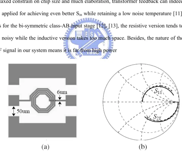
Fig. 3-8. Spiral inductor under test. (a) This 3.5-turn spiral inductor has its line
width set to 6um, the inner radius is 31um, and the line separation is 2um. (b) On the
Smith chart, the solid lines are the S11 and S21 from 0.1 to 20GHz provided by the vendor; the dashed lines are the simulated results. Capacitance of both the 50*50um2
input and output pads has been properly de-embedded.
Prior to the design of the Marchand balun, accuracy of the electromagnetic
simulation needs to be confirmed. Fig. 3-8 shows the S11 and S21 of a 3.5-turn spiral
inductor. The solid curves are provided by the vendor; the dashed curves are the
simulated results where 10Ω-cm resistance is chosen for the lossy silicon substrate,
the top-layer metal is 6um-wide, and the input and output pads capacitance has been
properly de-embedded. Fig. 3-9 shows the layout and schematic of the intended spiral
broadside-coupled Marchand balun where input port 1 is connected to the center of
one spiral, the output port 2 and port 3 are each extracted from the edge of the spiral.
Two tapered ground are needed to provide the short-circuited nodes on the center of
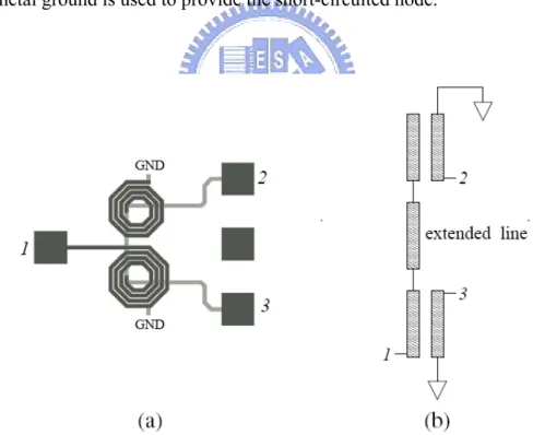
the spiral inductors. Fig. 3-10 is the alternative layout arrangement where the tapered
ground can be removed but an extended line has to be inserted between the center of
the two spiral inductors. As shown in Fig. 3-11, it can be easily demonstrated that the
Marchand balun with tapered ground is superior to the Marchand balun with extended
line. Table 3-12 is a simulation result summary of the proposed Marchand balun with
tapered ground compared with other published Marchand baluns, and the proposed
Marchand balun has 0.2 dB of magnitude difference and 2 degree of phase difference.
Fig. 3-9. Spiral broadside-coupled Marchand coupler. As indicated by the number,
the input port 1 is directly connected to the center of the spiral; the output port 2 and
port 3 are extracted from the edge of each spiral. At the center of each spiral, a
tapered metal ground is used to provide the short-circuited node.
Fig. 3-10. Spiral Marchand balun where the input port 1 is connected to the edge of
the spiral while the output ports are extracted from the center of each spiral. An
extended line has to be inserted between the center of the spirals for signal
connection.
Fig. 3-11. The simulated output magnitude and phase difference of the Marchand
balun. (a) Curve 1 is the output magnitude difference in dB of the Marchand balun
with taper ground; curve 2 is from the Marchand balun with extended line between the two spirals. The output ports are connected to 50Ω. (b) The corresponding phase
difference in degree.
Frequency Mag Error (dB) Phase Error (degree)
This Work 8~20GHz 0.2 2
[13] MTT-2006 4~16GHz 1~2 15
[19] MTT-2007 30~50GHz 0.2 1~2
[20] MTT-1998 1~5GHz 1.96 10.4
Table 3-12 A simulation result summary table of the proposed Marchand balun.
Compared with other published Marchand baluns, the proposed Marchand balun
indeed improved balanced performance.
Fig. 3-13 shows the input reflection coefficient Sin of the Marchand balun with
tapered ground. Curve 1 indicates that this balun will be matched over a wide
bandwidth if its output ports are each connected to 50Ω. In the real mixer circuit,
however, the output loading will much like a 0.13pF capacitor; thus, Sin will be
matched only at a specific frequency point, as indicated by curve 2 for the 0.13pF
case and the dashed curve 3 for the real mixer circuit.
As mentioned in [13], the s-parameter matrix of a balun is
[ ]
2 2 2 1 1 1 2 1 2 1 2 2 1 2 1 2 0 2 1 2 1 2 2 1 1 2 0 2 1 2 1 2 2 2 1 2 1 1 ( 1) 2 2 1 ( 1) 1 ( 1) 1 ( 1) 2 1 2 ( ) 1 2 2 2 1 ( 1) 1 ( 1) 1 ( 1) 2 1 2 ( ) 1 2 2 1 ( 1) 1 ( 1) 1 o o o o o o balun o o o o o z z z c c c c c z z z j j z z c c c z z z z c c c z c z S j j z z c c c z z z z z c c c z z c j z z c c c z z − − − + − + − + − + − − − = + − + − + − − − − + − + − + 1 1 2 o o z z z 1 2 ( 1) o z z ⎡ ⎤ ⎢ ⎥ ⎢ ⎥ ⎢ ⎥ ⎢ ⎥ ⎢ ⎥ ⎢ ⎥ ⎢ ⎥ ⎢ ⎥ ⎢ ⎥ ⎢ ⎥ ⎢ ⎥ ⎢ ⎥ ⎢ ⎥ ⎢ ⎥ ⎢ ⎥ − ⎢ ⎥ ⎢ ⎥ ⎣ ⎦The coupling factor c is set to
1 0 1 2 1 c z z = +
for optimum input impedance
matching. If all the ports are terminated with the same impedance, such as 50Ω, where
the impedance transforming ratio is unity, the required coupling factor c is -4.8 dB.
However if the loads are different, say 50Ω at unbalanced port and each a 0.13pF
capacitor at balanced ports, the required coupling factor is -8dB at 8GHz. Although
with the coupling factor -8dB, the input matching is optimized, the insertion loss (S21、S31) will degrade because of small coupling factor. It can be seen that when
Marchand balun is loaded with capacitors, the input matching and insertion loss will
be a trade-of. In many cases baluns are designed for 50Ω termination, and shown
wide-band input matching, but are not always capable for mixer application (capacitor
loading). In other words, Marchand balun under 50Ω termination with coupling factor
-4.8dB for a optimum input impedance matching has acceptable insertion loss. While
in designing Marchand balun under capacitance loading, input impedance matching
and insertion loss must be carefully arranged.
Of course, by inserting a RL circuit between the balun's output ports, a matched Sin
can be obtained over a wide bandwidth for capacitive loading [14]; however, this
lossy matching method will cause the deterioration of the RF signal. A better
approach, therefore, is our use of a single-stage transistor for wide-band matching.
Fig. 3-13. The simulated input reflection coefficient of the Marchand balun with
tapered ground. (a) Curve 1 is with each output port connected to a 50Ω resistor;
curve 2 is with each output port connected to a 0.13pF capacitor; the dashed curve 3 is
with each output port connected to the gate of the following stage transistor used in
the mixer. (b) The corresponding curves in Smith chart.
B. Mixing circuit design
To minimize the circuit's bias voltage Vbias, the drain current of the differential
pair is set to completely by-pass the four mixing transistors, as shown in Fig. 3-14.
And by operating these four mixing transistors as variable resistors where the
resistance is modulated by the LO signal, the biasing circuit can be greatly simplified
as both the drain and source of the transistors are now connected to ground through
large resistors. One plausible advantage of this resistive mixer is that it will have
small second-order intermodulation [15], though a detailed analysis on the CMOS
situation has not been carried out yet. The other advantage is that the equivalent
circuit for each of these mixing transistors will now be less frequency-dependency,
thus is more suitable for wide IF bandwidth application. In the simulation, a larger
conversion gain can indeed be observed when the drain bias is applied; however,
discernible conversion gain variation over the whole IF bandwidth restrains its
usefulness. Resistive mixer, on the other hand, tends to have constant conversion gain,
and is more straightforward in terms of biasing. Since the analysis of the mixers is
mostly limited to narrow IF bandwidth [16], its wideband counterpart needs to be
theorized too in our case, which means this part of the circuit is far from finished.
Fig. 3-14. Mixing circuit with LO injection. Each transistor's gate biasing circuit, i.e.
a large resistor connected to Vg, is omitted.
Fig. 3-15. Revised mixing circuit. By elevating the source and drain voltage of the
four mixing transistors to Vmixer = 0.7V and their gate voltage to 1.3Volt, the output
of the mixing circuit can be directly connected to the following IF circuit without
using the DC-blocking capacitors Cout.
C.
Output IF circuit design
Even being designated as IF, the 8.7GHz upper frequency of the IF bandwidth
prohibits the use of p-type transistors and thus some related analog-circuit techniques
for converting the differential-mode IF to single-end signal, as which will cause a
large conversion gain degradation as frequency increases. On the other hand, the
0.2GHz lower frequency of the IF band forbids the use of on-chip passive baluns. For
the purpose of low-frequency common-mode rejection ration, active balun made of
two n-type transistors is employed [17], [18]. As shown in Fig. 3-16, by neglecting
Cgs and Cgd at very low frequency there is
And so Vout will be zero for common-mode input signals if GAm = GBm and RAg =
RBg. To improve the common-mode rejection ratio at high frequency, a conventional
differential pair is added with its Ls Cs resonates at 9GHz, as shown in Fig. 3-17. For
output impedance matching and further gain boosting, another transistor is then used.
The large output DC-blocking capacitor CDC needs to be outside the circuit chip, as it
has to have small impedance at very low frequency. In improving the conversion
efficiency, one may wonder whether any of the inter-stage capacitors used in the IF
circuit can be removed. By replacing the Ls Cs with a current source, a differential
pair can indeed have good low-frequency common-mode rejection ratio. Therefore,
by having one high-frequency differential pair followed by another low-frequency
differential pair, the two inter-stage Cin can be omitted, as indicated by the arrow 1 in
Fig. 3-17, though this circuit needs a larger Vbias now. The reason for not using
active loading (where the drain of one p-type transistor is connected to its gate) for
further improving the low-frequency CMRR is because it will greatly sharpen gain
versus frequency response.
Fig. 3-16. The equivalent small-signal circuit of two transistor in cascade for
low-frequency common mode rejection.
Fig. 3-17. Output IF circuit. Each transistor's gate biasing sub-circuit is omitted. The
differential pair sub-circuit is responsible for high-frequency common-mode rejection
while the in-series sub-circuit is mainly for low-frequency response. The output
DC-blocking capacitor Cout is placed outside the silicon chip to allow the lowest
frequency output.
Another approach without using Cin is to have one n-type transistor (with source
degeneration) in parallel with a p-type transistor, as indicated by the arrow 2. Figs.
3-18, 3-19 are the simulated CMRR and voltage gain of these three different IF circuit
configuration. The IF circuit with curve 1 is made of one high-frequency differential
pair followed by two n-type transistors in cascade, and it apparently has the best
CMRR and a reasonably large differential-mode gain, and thus will be used in our
mixer design. The IF circuit with dashed curve 2 has both high-frequency and
low-frequency differential pairs; its inferior CMRR comes from its relatively large
common-mode voltage gain. The IF circuit with curve 3 has one high-frequency
differential pair followed by a n-type transistor in parallel with a p-type one; it has the
worst CMRR at low frequency and its differential-mode voltage gain is not large
enough too.
From Fig. 3-19a, it is apparent that a 20-30dB gain can be easily achieved if the IF
bandwidth is far less than 1GHz. Since this high IF-stage voltage gain may mask any
poor design of the front-end RF and mixing circuits, the large conversion gain may
not be a merit worth highlighting for narrow-IF-bandwidth mixers.
It can be seen that in Fig. 3-17 using a common source amplifier with resistor Rout
for output matching. By doing so it can achieve a wide band output matching and
provide gain for IF signal. However this will degrade linearity and disturb the output
spectrum. A compromised method is eliminated the common source amplifier.
Although it will loss some gain, the output return loss will still match due to the
common gate amplifier as show in Fig. 3-20.
Fig. 3-18. CMRR of the IF output stage. Curve 1 is from the circuit with
high-frequency differential pair followed by two n-type transistor in cascade; the
dashed curve 2 is from the circuit with both high-frequency and low-frequency
differential pairs; curve 3 is from the circuit with one high-frequency differential pair
followed by a n-type transistor and a p-type one in parallel.
Fig. 3-19. The differential-mode and common-mode voltage gain of the three
different IF output-stage circuits. (a) The common-mode gain. (b) The
differential-mode gain. The curve numbers are defined in previous figure.
Fig. 3-20. The modified mixer’s output stage for better linearity.
3.3 Simulated and Measured Results
A. Marchand balun
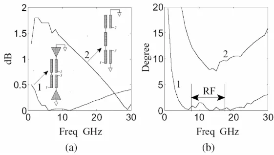
Fig. 3-21(a) is the layout of proposed balun, Balun-A, and Fig. 3-21(b) is the
simplified schematic of Balun-A, and Fig. 3-21(c) is the die photograph of Balun-A.
Balun-A is design for 8~17GHz with radius 50un and 3.5 turns, but without tapered
ground. It can be seen that without tapered ground Balun-A has two extra strip lines
connected the 1/4 λ coupled lines to ground. As it is expected, the new balun
implementation can shorten the extended line as mentioned before and can achieve
better performance. The simulation and measured results of Balun-A are shown in Fig.
3-22. The EM simulation time with PAD token long and as shown the phase and
magnitude error had the same result with simulation without PAD. Fig. 3-22 shows
Balun-A has magnitude error of 0.5dB and phase error of 6degree. The insertion loss
is -7dB for 8~17GHz which is acceptable for the proposed mixer.
(a)
(b)
Fig. 3-21. The proposed Balun-A. As showing in (a) is the ADS momentum
layout and in (b) is the simplified schematic. It can be seen that Balun-A without
tapered ground has two strip lines connected the 1/4 λ coupled lines to ground.
(c)
Fig. 3-21(c). The die photograph of Balun-A.
0 5 10 15 20 25 30 Frequency (GHz) 0 0.1 0.2 0.3 0.4 0.5 0.6 0.7 0.8 0.9 1 m a g n it u d e er ro r (d B ) EM without PAD Measurement EM with PAD
Fig. 3-22(a). Magnitude error of Balun-A.
0 5 10 15 20 25 30 Frequency (GHz) 0 1 2 3 4 5 6 7 8 9 10 P h ase er ro r (d eg ree) EM without PAD Measurement EM with PAD Fig. 3-22(b). Phase error of Balun-A.
0 5 10 15 20 25 30 Frequency (GHz) -14 -12 -10 -8 -6 -4 -2 0 R et u rn l o ss (d B ) EM without PAD Measurement EM with PAD
Fig. 3-22(c). Return loss of Balun-A.
0 5 10 15 20 25 30 Frequency (GHz) -20 -18 -16 -14 -12 -10 -8 -6 -4 In s e rt io n l o s s ( d B ) EM without PAD Measurement EM with PAD
Fig. 3-22(d). Insertion loss of Balun-A.
Table 3-22. Comparison of Simulated and Measured Results
Simulation Measurement
Process TSMC 0.18um COMS TSMC 0.18um COMS
Phase Error < 7 (degree) < 7 (degree)
Magnitude Error < 0.8 (dB) < 0.5 (dB)
Insertion Loss -7 (dB) -7.5 (dB)
B.
Mixer-A
The proposed mixer, Mixer-A, is an early edition and the schematic has shown in
Fig. 3-23. One difference between Mixer-A and the final edition circuit is that the LO
balun is implemented with LC shunt and parallel as shown in Fig. 3-24. This LC
combinational balun is for narrow band usage and the balun’s balance will degrade
with process variation. The other difference is the input and output matching using
on- board transmission lines W=2 mil, L=1650 um and W=3 mil, L=1000um for each.
Fig. 3-23. The schematic of Mixer-A.
Fig. 3-24. The schematic of LC balun.
Fig. 3-25(a) is the layout of Mixer-A and Fig.3-25(b) is the die photograph.
Although using two on-board microstrip lines for input and output matching, the chip
still designed for on-wafer measurement. CIC’s (Chip Implementation Centers’)
provides the on-wafer measurement and the measured equipments including a probe
station、 a network analyzer (HP8510C)、 a spectrum analyzer (Agilent E4407B)、
two signal generators, and several power supplies. Fig. 3-26 shows the arrangement of
DC and RF probes (one 6-pin DC probe and three 3-pin RF probe with pitch 100um).
The measurement of S-parameter is shown in Fig. 3-27. Fig. 3-28 and Fig. 3-29 are
the measurement of conversion gain and IIP3.
Fig. 3-25(a). The layout of Mixer-A. Chip size: 1.13×1.17 mm2.
Fig. 3-25(b). The chip die photograph.
Fig. 3-26. Arrangement of DC and RF probes. Three 3-pin probes with pitch 100um
for RF signals and one 6-pin probe with pitch 100um for DC bias.
Fig. 3-27. The measured arrangement of S-parameter.
Fig. 3-28. The measured arrangement of conversion gain.
Fig. 3-29. The measured arrangement of IIP3.
Mixer-A is designed with TSMC 0.18um mixed-signal/RF CMOS process, chip size 1.13×1.17 um2, power consumption 37mW. The S-parameter is shown in Fig.
3-30(a~c), where in Fig. 3-30(a) the RF Port return loss < 7dB because omitting the
two matching microstrip lines. Due to the input output poor matching, the conversion
gain will degrade 1~2 dB. Shown in Fig. 3-30(b) is the LO Port return loss, and at
fixed LO frequency 17.5 GHz, the return loss is -15dB. As shown in Fig. 3-30(c) the
IF port return loss is below -10dB within IF bandwidth 0.5~9GHz.
0 2 4 6 8 10 12 14 16 18 20 Frequency (GHz) -12 -10 -8 -6 -4 -2 0 R F P o rt Re tu rn L o s s ( d B ) Simulation Measurement
Fig. 3-30(a). RF Port return loss for RF signal from 8.5~17GHz.
0 2 4 6 8 10 12 14 16 18 20 Frequency (GHz) -30 -25 -20 -15 -10 -5 0 L O P o rt R e tu rn L o s s ( d B ) Measurement Simulation Fig. 3-30(b). LO port return loss for a fixed LO frequency 17.5GHz.
0 2 4 6 8 10 12 14 16 18 20 Frequency (GHz) -20 -18 -16 -14 -12 -10 -8 -6 IF P or t R e tur n Los s ( dB ) Measurement Simulation
Fig. 3-30(c). IF port return loss for IF frequency 0.5~9GHz.
As shown in Fig. 3-31, the conversion gain is -6dB with LO at fixed 17GHz and the
IF band is 11GHz (6~17GHz). In Fig. 3-32 the RF to IF isolation is under -30dB. The
isolation is an important factor because in the input port of the mixer the out of band
RF signal (0.5~8GHz) will through the mixer to output to disrupt the IF-band signal.
0 2 4 6 8 10 12 14 16 18 RF Frequency (GHz) -120 -100 -80 -60 -40 -20 0 C onv e rt ion G a in (dB ) Measurement Simulation
Fig. 3-31. Conversion gain of Mixer-A whit LO at 17.5GHz.
0 2 4 6 8 10 12 14 16 18 Frequency (GHz) -110 -100 -90 -80 -70 -60 -50 -40 -30 -20 -10 0 R F t o I F I s o la ti o n ( d B ) Measurement Simulation
Fig. 3-32. Isolation of Mixer-A.
As shown in Fig. 3-33(a)~(c) the IIP3 is 5dB and this will imply that the mixer has
high linearity and keep such wideband IF signal from distortion.
(a) IIP3=1dBm with RF frequency @ 8GHz. (b) IIP3=7dBm with RF frequency @ 12GHz
(c) IIP3=9dBm with RF frequency @ 16GHz
Fig. 3-33(a)~(c). IIP3 of Mixer-A.
The comparison of simulated and measured results is shown in Table 3-34.
Although the simulating and measuring results are consisting, the conversion gain is
unsatisfied. It can be seen that due to the double balanced Gilbert cell structure, the
LO differential signal will affect the conversion gain. The balance of differential
signal will affect the voltage of differential-out signal. Therefore in order to improve
the LO differential signal under the process variation, the LC structure is taken the
place of Marchand balun. This is because the capacitor’s process variation is more
severe and the Marchand balun’s wideband performance can tolerant more variation.
The improved mixer, mixer-B, will shown later and can be seen that the conversion
gain improvement is 8dB.
Table 3-34. Comparison of Mixer-A’s simulated and measured results.
Simulation Measurement
Process CMOS 0.18um CMOS 0.18um
RF Bandwidth 8.5~17GHz 8.5~17GHz
Supply Voltage(V) 1.8 1.8
IF Bandwidth 0.5~9 GHz 0.5~9 GHz
RF input return loss < -7 (dB) < -8 (dB)
LO input return loss < -15 (dB) < -15 (dB)
IF input return loss < -10 (dB) < -10 (dB)
Conversion Gain (dB) -6 -6
RF to IF Isolation < -20 (dB) < -40 (dB)
IIP3 7dBm@12GHz 7dBm@12GHz
Power (mW) 41 38
C. Mixer-B
The schematic of Mixer-B is shown in Fig. 3-35. As indicated by arrow1, the
on-chip inductor is for input matching. Using Marchand balun to transform the single
LO signal to differential pair, the balance is less dependent to process variation. The
layout is shown in Fig. 3-36 where the chip size is 0.9*1.46 um2.
Fig. 3-35. The schematic of Mixer-B.
Fig. 3-36. The layout of Mixer-B. Chip size 0.9*1.46 um2.
As shown in Fig. 3-37, by using the on-chip inductor for input matching, the RF
port return loss is under -10dB for 8.5~17GHz. In Fig.3-38 and Fig.3-39 are the LO
and IF ports’ return loss, and shown the return loss is under -10dB for the desired
bandwidth.
Fig. 3-37. RF port return loss for RF signal band 8.5~17GHz.
Fig. 3-38. LO port return loss for a fixed LO frequency at 17.5GHz.
Fig. 3-39. IF port return loss for IF band 0.5~9GHz.
The conversion gain is shown in Fig.3-40,and the gain variation is less than 3dB for the RF bandwidth. The three corner (TT、FF、SS) are simulated under the same current
consumption, and the three conversion gains are acceptable.
Fig. 3-40. Conversion gain versus RF frequency with LO at 17.5GHz.
The isolation from RF port to IF port is shown in Fig.3-41, and the isolation is
-30dB in RF bandwidth. It means that the lower out of RF band signal has 30dB
rejection ratio to IF port. This can release the loading of the filters connected to the
mixer.
Fig. 3-41. Isolation of RF port to IF port.
Table 3-42. The summary of Mixer-B.
Simulation
Process CMOS 0.18um
RF Bandwidth 8.5~17 GHz
Supply Voltage(V) 1.8
IF Bandwidth 0.5~9 GHz
RF input return loss < -10 (dB)
LO input return loss < -15 (dB)
IF input return loss < -10 (dB)
Conversion Gain 7 dB (dB)
RF to IF Isolation < -30 dB (dB)
Power (mW) 37
3.4
Reference
[1] L. A. MacEachern, T. Manku, .A charge-injection method for Gilbert cell biasing,.
IEEE Canadian Conference on Electrical and Computer Engineering, vol. 1, pp.
365.367, May 1998.
[2] M. L. Schmatz, U. Lott, W. Baumberger, W. Baechtold, .Novel design topology
for ultra low power down converters with broadband ob chip matching network,.
IEEE Trans. Microwave Theory Techniques, vol. 43,no. 12, pp. 2946.2951, Dec.
1995.
[3] S. J. Mahon, et. al, .Broadband integrated millimeter-wave up- anddown-converter
GaAs MMICs,. IEEE Trans. Microwave Theory Techniques, vol. 54, no. 5, pp.
2050.2060, May 2006.
[4] T. T. Hsu, C. N. Kuo, .Low power 8-GHz ultra-wideband active balun,. IEEE
2006 Topical Meeting on Silicon Monolithic Integrated Circuits inRF systems, pp.
365.368, Jan. 2006.
[5] R. Hu, .Wide-band matched LNA design using transistor's intrinsic gate-drain
capacitance,. IEEE Trans. Microwave Theory Techniques, vol. 54,no. 3, pp.
1277.1286, March 2006.
[6] B. W. Lee, D. S. Park, S. S. Park, M. C. Park, .Design of new three-line balun and
its implementation using multilayer configuration,. IEEETrans. Microwave Theory
Techniques, vol. 54, no. 4, pp. 1405.1414, April2006.
[7] W. M. Fathelbab, M. B. Steer, .New classes of miniaturized planar baluns,. IEEE
Trans. Microwave Theory Techniques, vol. 53, no. 4, pp.1211.1220, April 2005.
[8] T.-Y. Yang, H.-K. Chiou, .A 16.46 GHz mixer using broadband multilayer balun
in 0.18-um CMOS technology,. IEEE Microwave Wireless Comp .Lett., vol. 17, no. 7,
pp. 534.536, July 2007.
[9] N. Marchand, .Transmission-line conversion transformers,. Electronics, vol. 17,
no. 12, pp. 142.145, Dec. 1944.
[10] K. S. Ang, I. D. Robertson .Analysis and design of impedance-transforming
planar Marchand baluns,. IEEE Trans. Microwave Theory Techniques, vol. 49, no. 2,
pp. 402.406, Feb. 2001.
[11] C. T. Fu, C. N. Kuo, .3.11-GHz CMOS UWB LNA using dual feedback for
broadband matching,. 2006 IEEE Radio Frequency Integrated Circuits Symposium,
pp. 53.56, June. 2006.
[12] B. Gilbert, .The MICROMIXER: a highly linear variant of the Gilbert mixer
using a bisymmetric class-AB input stage,. IEEE J. Solid-State Circuits, vol. 32, pp.
1412.1423, Sep. 1997.
[13] S. C. Tseng, C. C. Meng, C. H. Chang, C. K. Wu, G. W. Huang,. Monolithic
broadband Gilbert micromixer with an integrated Marchand balun using standard
silicon IC process,. IEEE Trans. Microwave Theory Techniques, vol. 54, no. 12, pp.
4362.4371, Dec. 2006.
[14] K. W. Hamid, A. P. Freundorfer, Y. M. M. Antar, .A monolithic double-balanced
circuit conversion mixer with an integrated wideband passive balun,. IEEE J.
Solid-State Circuits, vol. 40, no. 3, pp. 622.629, March 2005.
[15] S. A. Maas, .A GaAs MESFET mixer with very low intermodulation,. IEEE
Trans. Microwave Theory Techniques, vol. mtt-35, no. 4, pp. 425. 429, Apr. 1987.
[16] R. A. Pucel, D. Masse, .Performance of GaAs MESFET mixers at X band,. IEEE
Trans. Microwave Theory Techniques, vol. mtt-24, no. 6, pp. 351.360, June 1976.
[17] H. Ma, S. J. Fang, F. Lin, K. S. Tan, .A high performance GaAs MMIC
upconverter with an automatic gain control amplifier,. 19th Annual Gallium Arsenide
Integrated Circuit Symposium, pp. 232.235, Oct. 1997.
[18] R. H. Lee, et. al., .Circuit techniques to improve the linearity of an up-conversion
double balanced mixer with an active balun,. 2005 Asia Pacific Microwave
Conference (APMC), vol. 2, pp. 4.7, Dec. 2005.
[19] Chin-Shen Lin; Pei-Si Wu; Mei-Chao Yeh; Jia-Shiang Fu; Hong-Yeh Chang;
Kun-You Lin; Huei Wang; ”Analysis of Multiconductor Coupled-Line Marchand
Baluns for Miniature MMIC Design”, Microwave Theory and Techniques, IEEE
Transactions on olume 55, Issue 6, Part 1, June 2007 Page(s):1190 - 1199
[20] Choonsik Cho; Gupta, K.C.,”A new design procedure for single-layer and
two-layer three-line baluns”, Microwave Theory and Techniques, IEEE Transactions
on lume 46, Issue 12, Part 2, Dec. 1998 Page(s):2514 - 2519
Chapter 4
Conclusion and Future Work
4.1
Conclusion and Future Work
The thesis mainly contains two circuits; one is transformer feedback LNA, and the
other is wide IF band down-converting mixer. For LNA, using transformer feedback
to achieve input matching can eliminate the noise of input port. Because the
transformer feedback can simply the input-matching schematic and thus only the
noise of input transistor exist. Form the simulated results the noise figure of the
proposed LNA is 3dB from 10~18GHz with 17dB voltage gain. However the
simulated results need the measured results to verify and the 37.6mW power
consumption can be further minimized. Besides, the input impedance of transformer
feedback still need accurately development since for high frequency, the transistor’s
parasitic capacitor Cgd can no longer be ignored in derivation of input impedance.
For the wide IF band down-converting mixer, two components still need to be
further analyzed; one is the balun’s input impedance and the other is mixer core.
Mentioned in [1], the S-parameter of Marchand balun is as follows, and the matrix
derived with the assumption that the two coupled lines have electric length θ=900 is
valid only for the central frequency. When using Marchand balun in wideband
application, the wideband S-parameter of Marchand balun is needed. Since Marchand
balun is composed of two quarter-λ coupled lines, analysis of a single coupled line for
wide band is approachable. Then using ABCD matrix multiplication of two single
coupled lines can form the matrix of Marchand balun.